Analysis of the role of mobility-lifetime products in the performance
of amorphous silicon
p-i-n
solar cells
J. M. Asensi,a)J. Merten, C. Voz, and J. Andreu
Departament de Fı´sica Aplicada i Optica, Universitat de Barcelona, Avinguda Diagonal 647, Planta 4, E-08028 Barcelona, Spain
~Received 13 October 1998; accepted for publication 30 November 1998!
An analytical model of an amorphous silicon p-i-n solar cell is presented to describe its photovoltaic behavior under short-circuit conditions. It has been developed from the analysis of numerical simulation results. These results reproduce the experimental illumination dependence of short-circuit resistance, which is the reciprocal slope of the I(V) curve at the short-circuit point. The recombination rate profiles show that recombination in the regions of charged defects near the p-i and i-n interfaces should not be overlooked. Based on the interpretation of the numerical solutions, we deduce analytical expressions for the recombination current and short-circuit resistance. These expressions are given as a function of an effectivemt product, which depends on the intensity of illumination. We also study the effect of surface recombination with simple expressions that describe its influence on current loss and short-circuit resistance. © 1999 American Institute of Physics. @S0021-8979~99!03705-6#
I. INTRODUCTION
The collection mechanism in a-Si:H-based p-i-n solar cells can be studied theoretically by means of numerical1–3 and analytical models4,5. Numerical treatments using com-puter calculation have often been preferred due to the diffi-culty of solving the fundamental formulas for analysis ~Pois-son and continuity equations!. However, the interpretation of the experimental behavior of the cell from numerical results is often complicated by the large number of parameters in-volved. Furthermore, many of the material parameters re-quired are experimentally inaccessible or imperfectly known. Analytical models have the drawback of requiring strong as-sumptions in order to solve the transport equations, but the simplicity of their solutions allows a straightforward link with the experimental results.
There have been fewer fully analytical attempts to de-scribe the collection mechanism in a-Si:H p-i-n solar cells than numerical treatments. The main attempt is probably the uniform-field model of Crandall,4 whose main assumptions are: constant electric field, negligible diffusion in the i layer, and the use of the Shockley–Read–Hall expression for re-combination as derived for a two-state rere-combination center. These assumptions lead to a very simple expression for the photocurrent as a function of the two carrier drift lengths. Later, Hubin and Shah5 proposed a variation of Crandall’s model, in which a more realistic description of recombina-tion in a-Si:H is introduced. They consider the amphoteric nature of the dangling bond, the main recombination center in a-Si:H, and use a recombination function based on a single type of three-state recombination center. In this way, they explain some of the differences between Crandall’s ana-lytical results and the more realistic models based on numeri-cal simulation:1for example, this treatment shows that it is
the carrier with the shorter drift length that will determine collection.
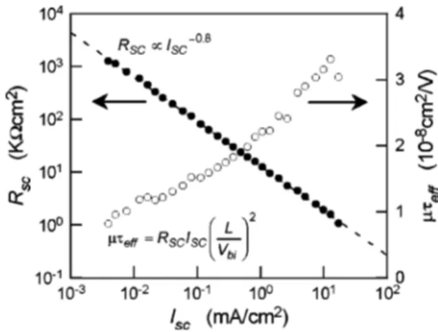
Recently, we used the uniform-field model of Hubin and Shah to interpret the variable illumination measurement of the short-circuit resistance Rscof a-Si:H p-i-n solar cells:6
i.e., the reciprocal slope (dV/dI)V50of the I(V) curve at the short-circuit point. Over a wide range of illumination levels, Rscis inversely proportional to the short-circuit current Isc. In this situation, the Rsc value is related to the
voltage-dependent photocurrent collection and can be calculated by the uniform-field theory. Thus, if Rscis plotted as a function
of Isc, it is possible to extract the value of an effective mt
product which suitably combines the mt products of elec-trons and holes in the layer ~more recently, other authors7 reported a study which is similar but based on the Crandall theory!.
Although the method is straightforward and has been satisfactorily applied as a quantifying tool for the state of degradation of a-Si:H solar cells and modules,6some experi-mental results question the validity of the uniform-field model used to interpret variable illumination measurements:
~a! In general, themteffvalue deduced from Rscapplying
the uniform-field model is significantly lower ~by up to 1 order of magnitude! than the one obtained from photocon-ductivity in intrinsic material.
~b! The Rscdependence on illumination level is
quasilin-eal: in most samples Rsc}Iscg whereg,1 is found. In fact, if the value of mteff, deduced applying the uniform-field model @see Eq. ~10! in Sec. II! is plotted as a function of Isc,mteff increases as the illumination level increases ~see
Fig. 1!.
In this article, numerical simulation is used to show that these effects could be correlated with the charged defect states which necessarily exist near the p-i and i-n interfaces. For low and intermediate illumination levels, most of the recombination occurs in these regions. When illumination is
a!Electronic mail: [email protected]
2939
increased~for Isc.10 mA/cm2), the charged defects are
neu-tralized and the importance of the recombination near the interfaces decreases. Only in this case of high illumination are the uniform-field model assumptions valid. From the nu-merical results we develop a more detailed analytical scription of collection in p-i-n a-Si:H solar cells. Our de-scription includes the prominent role of charged defects in the i layer and enables a more general mteffdepending on
light intensity to be defined.
The paper is organized as follows. In Sec. II, we review the assumptions of the uniform-field model of Shah and Hu-bin, and show the expression deduced for short-circuit resis-tance Rscas a function of the standard effectivemt product.
In Sec. III, we describe our numerical model and present the full set of equations used in the computer simulation. Our numerical treatment was simplified for a better comparison with the results of the uniform-field model description. We then simulate a variable illumination measurement of Rscand show that recombination in the charged regions at interfaces is not negligible. In Sec. IV we present the analytical de-scription of the p-i-n solar cell including the effect of the charged regions. We show that, in thermodynamic equilib-rium, the electric field profile, and the widths of the charged regions near the p-i and i-n interfaces can be deduced em-ploying dangling bond statistics. In particular, we show that the use of the ‘‘thin solar cell’’ approach leads to straight-forward expressions. We then study the effect of illumin-ation on the electric field, carrier density, and recombinillumin-ation profiles. From this analysis the recombination current and the short-circuit resistance can be given as a function of a new effective mt product which adequately combines the effect of the different regions on the i layer. Section IV closes with an analysis of the influence of surface recombi-nation.
II. UNIFORM-FIELD MODEL ANDmt PRODUCT
Hubin and Shah5solved the problem of bulk collection in a p-i-n solar cell under these three basic assumptions:
~a! constant electric field in the i layer, ~b! negligible diffusion in the i layer,
~c! bulk recombination in the i layer is determined by the
neutral dangling bonds.
The two first assumptions are indeed applicable to thin p-i-n cells under small or negative voltage bias. These are the same restrictive assumptions as in Crandall’s model. To deal with recombination by neutral dangling bonds, they in-troduce a linear approximation for the recombination func-tion associated with a single type of recombinafunc-tion center that can exist in three charge states:8
RDB5
n tn01
p
tp0, ~1!
where n and p are the densities of free carriers~electrons and holes! andtn0 andtp0 are the capture times of free electrons and free holes, respectively, by neutral dangling bonds. The capture times are defined by
tn05~v thsn0NDB!21 ~2! and tp05~v thsp0NDB!21,
where sn0 andsp0 are the capture cross sections of the free carriers by the neutral dangling bonds, NDBis the total
den-sity of dangling bonds, andvthis the thermal velocity.
Now, assuming a uniform generation rate G due to weakly absorbed light, the steady-state continuity and trans-port equations with the appropriate boundary conditions can be solved and the densities of free carriers as a function of the position x in the i layer can be obtained. On introducing n(x) and p(x) into Eq.~1!, the total recombination in the i layer can be calculated, and from this the bulk collection x
~i.e., the fraction of the collected photocurrent divided by the
total generation current in the i layer!. Hubin and Shah found
x5L1 l lnlp nexp~L/LC!2lpexp~2L/LC! 3
F
expS
L LCD
2expS
2 L LCDG
, ~3!where L is the thickness of the i layer and LC is the collec-tion length:
LC52 lnlp ln2lp
, ~4!
where ln and lp are the drift lengths for free electrons and free holes. These lengths depend on the electric field in the i layer (Ei), the band mobilities for free carriers (mnandmp), and the capture times of free carriers by neutral dangling bonds (tn0 andtp0): ln5mntn 0uE iu ~5! and lp5mptp0uEiu.
In the case of a thin p-i-n device, the electric field strength is strong enough for the drift lengths to be much larger than the i layer thickness. Then Eq.~3! becomes
FIG. 1. Variable irradiance measurement of Rscin a-Si:H p-i-n solar cells.
x5 LC*
LC*1L, ~6!
where LC* is a redefinition of the collection length as LC*52 lnlp
ln1lp5mteffuEiu, ~7!
wheremteffis an effectivemt product which suitably
com-binesmt products of electrons and holes: mteff52
mntn0 •mptp0
mntn01mptp0. ~8!
It can be shown that if ln'lpthen Eq.~6! is also valid in the more general situation, i.e., when the drift lengths ln and lpare comparable to or shorter than the i layer thickness~see Ref. 5!. Note that in this case LC*'ln'lp.
In accordance with Eq.~6! the loss current Irecin the i
layer can be expressed as
Irec5 L LC*Iph5 L2 mteff~Vbi2V! Iph, ~9!
where Iph is the generation current in the i layer (Iph 5qGL), Vbi is the built-in voltage, and V is the applied
voltage.
In the short-circuit region, and neglecting the effect of ‘‘parasite’’ resistance ~see Ref. 6!, the slope of the I(V) curve is determined by the voltage dependence of Irec. Thus,
differentiating Eq.~9! with respect to the applied voltage, the short-circuit resistance can be deduced:
Rsc'
S
dV dIrecD
V505mteffS
Vbi LD
2 Isc21, ~10!where the generation current Iphis approximated to the
short-circuit current Isc~note that we assumex'1). So if we plot
Rsc as a function of Isc it is possible to extract, from the region where Rscis inversely proportional to Isc, the value of mteff.
III. NUMERICAL SIMULATION A. Simplifying assumptions
All numerical calculations in this article were carried out using the simulation model which was previously developed by our group.3Our computer program uses finite differences and the Newton technique to solve Poisson’s equation and continuity equations for the complete diode. The flexibility of the program allows different model assumptions to be analyzed. Our aim here is to study the validity of the hypoth-eses of the uniform-field model@assumptions ~a!, ~b! and ~c!, in Sec. II# that lead to Eqs. ~9! and ~10! for the recombina-tion current and short-circuit resistance, respectively. There-fore, as an excessively detailed description of the diode could complicate the analysis, some simplifying assumptions were incorporated into the numerical treatment:
~a! The transport equations were solved only within the
intrinsic layer, and boundary conditions were defined at the doped-layer/intrinsic-layer interfaces ( p-i and i-n). This
as-sumption reduces significantly the number of physical pa-rameters involved: as will be shown later, the doped-layer influence is completely described by only five i layer bound-ary condition parameters.
~b! To find the trapped charge density and the
recombi-nation rate, only the dangling bonds were examined. This is a good assumption for the middle of the i layer, but is inad-equate for the regions near the interfaces p-i and i-n, where the Fermi level significantly enters the tail states. However, the tail states mainly affect the trapped charge near the inter-faces and are thought to create only a small distortion in the magnitude of the electric field. A similar effect is produced by the fixed space charge at the interfaces in the doped lay-ers. In fact, these two effects can be included as a reduction of the built-in potential Vbi, one of the boundary conditions
of the problem.
~c! The defect distribution throughout the i layer was
assumed uniform and constant. This is the standard model of the density of states in a-Si:H~and a normal assumption for all uniform-field models!. A further simplification is to as-sume that the defect states in the gap are discrete.
B. Model equations
The equations that must be solved numerically are Pois-son’s equation:
dE dx5
q
« @~p2n!1Q~p,n!#, ~11!
relating the derivative of the electric field E to the local charge~free electrons n, free holes p, and trapped charge Q); the current density equations, combining the two driving forces of carrier movement, drift and diffusion, with the total hole ( jp) and electron ( jn) currents:
jp~x!5qmpp~x!E~x!2kTmp d p~x! dx , ~12a! jn~x!5qmnn~x!E~x!1kTmn dn~x! dx , ~12b!
and the two continuity equations: d jp~x!
dx 5q@G2R~p,n!#, ~13a!
d jn~x!
dx 52q@G2R~p,n!#, ~13b!
where G is the generation rate and R( p,n) is the recombina-tion rate.
As stated, we assume that the trapped charge and the recombination are only determined by dangling bonds. Thus, the trapped charge Q is
Q5@ f1~p,n!2 f2~p,n!#NDB, ~14!
where NDBis the constant density of dangling bonds in the i
layer and f1 and f2 are the occupation of the positive and negative dangling-bond states:2
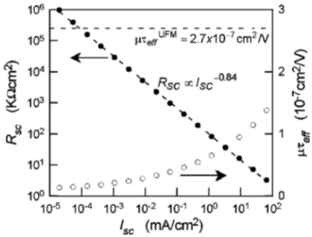
f1~p,n!5 T 1~p,n! 11T1~p,n!1T2~p,n!, ~15a! f2~p,n!5 T 2~p,n! 11T1~p,n!1T2~p,n!, ~15b! with T1~p,n!5sp 0 p1 12sn1NCe2~EC2E 1!/kT sn1n12sp0N Ve2~E 12E V!/kT, ~16a! T2~p,n!5sn 0n1 1 2s2pNVe2~E 22E V!/kT sp2p12sn0 NCe2~EC2E 2!/kT, ~16b!
wheresn0 andsp0 are the capture cross sections of electrons and holes by neutral dangling bonds,sn1is the capture cross section of electrons by positive dangling bonds, sp2 is the capture cross section of holes by negative dangling bonds, and E1 and E2 are the effective energy levels of the D1↔D0 and D2↔D0 transitions.
The rate of recombination via dangling bonds is given by R5vth~pn2ni 2!
S
sn 1s p 0 sn1n12sp 0 NVe2~E 12E V!/kT 1 sp2sn 0 sp2n12sn0N Ce2~EC2E 2!/kTD
f0~p,n!NDB, ~17!where ni is the equilibrium intrinsic concentration and f0 is the occupation of the neutral dangling bonds:
f0~p,n!5 1
11T1~p,n!1T2~p,n!. ~18! Finally, this set of coupled differential equations must be solved with the appropriate boundary conditions. As stated above, these conditions are defined at the interfaces p-i and i-n. The first boundary condition refers to the potential differ-ence across the i layer:
V~L!2V~0!5Vbi2Vext, ~19!
where Vbiis the built-in potential, i.e., the difference in the
electrostatic potential between the p layer and the n layer in equilibrium, and Vextis the applied voltage. Note that the full built-in voltage is assumed to be applied over the i layer alone, and that the part of the potential lost in the doped layer space-charge regions is neglected.
The remaining boundary conditions define the current densities at the interfaces by effective surface-recombination velocities S for both holes and electrons. However, some simplification is possible: e.g., for majority carriers we can assume that the interfaces behave as ohmic contacts, and the corresponding S values are very high. Therefore, we can as-sume a constant majority-carrier concentration that is inde-pendent of the current density:
p~0!5peq~0!
~20!
and
n~L!5neq~L!,
where peq(0) and neq(L) are the equilibrium hole and
elec-tron densities in the doped layers. For the minority-carrier currents @ jp(L) and jn(0)] we use the more general form:
jp~L!5qSL@p~L!2peq~L!#, ~21a!
jn~0!5qS0@n~0!2neq~0!#, ~21b!
where peq(L) and neq(0) are the equilibrium minority-carrier
densities in the doped layers, and SLand S0are the interface
recombination velocities for the minority carriers at the in-terfaces. Note that the currents given by Eq. ~21! are loss currents. The case SL5S050 is an ideal situation where the
interfaces are perfectly blocking contacts for the minority carriers.
C. Simulation results
Variable irradiance measurement of Rscover a range of illumination levels from 1025 to 102 mA/cm2 ~for Isc) was
simulated. It was considered uniform-light illumination. The device simulated was a 0.3-mm-thick a-Si:H solar cell. Model parameters are listed in Table I. These parameters are the typical ones for a-Si:H material in the annealed state
~e.g., see Ref. 9!: with these parameters and using Eq. ~8! we
obtain a mteffvalue of 2.731027 cm2/V, and applying Eq. ~7! we find 62mm for the collection length LC*~note that this
is much longer than the i layer thickness L).
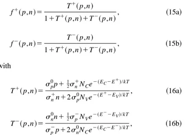
Figure 2 shows the calculated short-circuit resistance Rsc
and the mteff, deduced from Rscby applying Eq. ~10! as a
function of the short-circuit current Isc. At the lowest
illu-TABLE I. Values of parameters used for numerical calculations.
Principal intrinsic material parameters
Band gap Eg~eV! 1.77
Effective densities of states NCand NV(cm23) 431019
Electron mobilitymn(cm2/V/ s) 10
Hole mobilitymp(cm2/V/ s! 4
Dangling bond density NDB(cm23) 10 16
Energy level of the D1↔D0transition E12E
V~eV! 0.735
Effective correlation energy Ueff~eV! 0.3
Capture cross-section of electrons by D0sn
0
(cm2) 5310216 Capture cross-section of electrons by D1sn1(cm
2) 2.5310214
Capture cross-section of holes by D0sp
0
(cm2) 10216 Capture cross-section of holes by D2sp2(cm
2) 5310215
Capture times of free carriers by dangling bonds Capture time of electrons by D0t
n
05(v thsn
0NDB
~)21~s! 231028 Capture time of electrons by D1tn15(vthsn1NDB)21~s! 4310210
Capture time of holes by D0t
p
05(v thsp
0NDB)21~s! 1027
Capture time of holes by D2tp25(vthsp2NDB)21~s! 231029
Doped material parameters
Fermi-level in the p-layer EF2EV~eV! 0.58
Fermi-level in the n-layer EC2EF~eV! 0.58
Interface recombination velocity of minority carriers SL
and S0~cm/s!
mination levels we find a value of mteffapproximately one order of magnitude smaller that predicted by the uniform-field theory. On the illumination level increasing, this differ-ence decreases and the mteffis close to the value
theoreti-cally predicted. In fact, one can see from Fig. 2 that the Rsc
dependence on illumination is quasilineal: we find Rsc}Iscg with g50.84. These results are consistent with the experi-mental data~see Fig. 1!. Consequently, a detailed analysis of our simulation results is expected to reveal aspects of the physics of the device that are not included in the conven-tional uniform-field model.
Figure 3 shows some calculated profiles ~density of trapped charge, electric field, and recombination rate! at short-circuit conditions for two different levels of illumina-tion. The most important differences between simulation and the uniform-field model suppositions appear in the low-illumination regime ~solid line in Fig. 3!. In this regime, neutrality is only maintained in a small region within the i layer. In the regions near to the doped zones, dangling bonds are charged@Fig. 3~A!#, altering the electric field @Fig. 3~B!# and clearly the recombination profile @Fig. 3~C!# . It can be observed that, in this case of low illumination, most of the recombination occurs close to the interfaces where the de-fects are in the charged state. So the collection, and probably its dependence on the applied voltage, must be controlled by these regions. When illumination increases, the neutral re-gion increases and the charged rere-gions shrink~dashed line in Fig. 3!. The field inside the bulk of the i layer grows and the relative weight of the recombination through charged dan-gling bonds becomes much lower: note that only in the re-gime of very high illumination (Isc.102mA/cm2) could
hy-potheses~a! and ~c! of the uniform-field model be considered valid.
Now we shift our attention to hypothesis ~b! of the uniform-field model, i.e., that photocarrier transport occurs by field-assisted drift. Figure 4 shows the drift and the dif-fusion components of the hole current density under short-circuit conditions for the two cases of illumination. It can be seen that near the p-i interface, where holes are the majority carriers, both drift and diffusion contribute to the
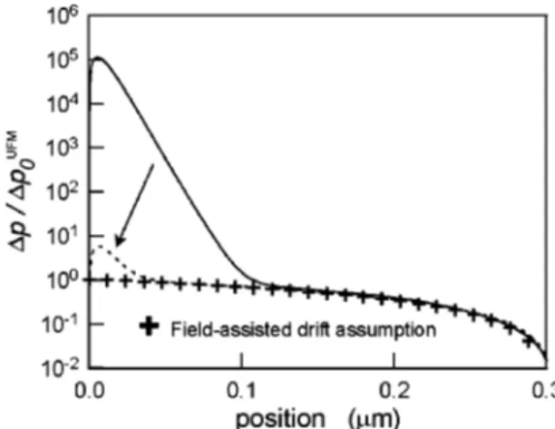
photocur-rent. Therefore, diffusion cannot be overlooked when solving the hole transport equations in this region. As can also be seen, this effect decreases under very intense illumination and, only in this case, hypothesis ~b! of the uniform-field model could be applied in the whole bulk of the i layer. To demonstrate more clearly that diffusion must be included for majority carriers close to the interfaces, in Fig. 5 we compare the profile of photogenerated hole density with the profile deduced from the uniform-field theory which overlooks dif-fusion@see Eq. ~31! in Sec. IV C#. It can be seen that, at low
FIG. 2. Simulated short-circuit resistance Rscas a function of the
short-circuit current Isc. The value ofmteffdeduced from Rscby applying Eq.
~10! and the theoretical value ofmteffdeduced from~8! ~dashed line! are
shown.
FIG. 3. Simulated profiles of ~A! density of trapped charge, ~B! electric field, and~C! recombination rate normalized to generation, at short-circuit conditions and for two illumination levels: low ~solid line, Isc
51023 mA/cm2) and high ~dashed line, I
sc5102 mA/cm2). The arrows
indicate evolution with illumination.
FIG. 4. Simulated profiles of the hole current density normalized to the total short-circuit current in the same conditions as in Fig. 3. The drift and the diffusion components of the current and the effect of the illumination level are shown.
illumination, the simulated photohole density at the p-i inter-face is significantly different from the theoretical value. As will be discussed later, the majority-carrier densities photo-generated near the interfaces are very sensitive to perturba-tions in the electric field~which could be due to illumination and/or voltage bias!. Although this is not significant in cal-culating the loss of carrier collection, since recombination in these regions is determined by minority carriers, the com-plete description of the p-i-n diode must take into account the effect of the majority carriers injected from the p-i and i-n contacts.
In summary, numerical simulation has demonstrated that hypotheses used in the uniform-field model are not fulfilled, especially at low illumination. A correct interpretation of Rsc
measurement or, in general, of collection in amorphous p-i-n solar cells must include the state of charge of the defects in the regions close to the doped zones and, probably, the effect of the diffusion current. This is the theme of Sec. IV.
IV. ANALYTICAL DESCRIPTION A. Equilibrium
In thermodynamic equilibrium, i.e., in the dark and with-out external voltage, the regions near the p-i and i-n inter-faces are non-neutral due to the Fermi level shifts in these regions. In Fig. 6, where the band diagram of a p-i-n struc-ture is shown, we can see the different regions in the intrinsic layer. Assuming discrete transition levels for the dangling bonds and using the zero-temperature approximation, three regions within the intrinsic layer can be identified, which vary according to the position of the Fermi level:
~A! Interface region ~PI!: between x50 and x5xp, where xp is the i layer position where Ef is on the dangling bond level E1. All defects are positively ionized. The poten-tial variation Vp across the PI region is determined by the difference between the Fermi level position in the p-doped material and the E1 level of the dangling bond. The electric field strength decreases as a consequence of the defect charge:
E~x!5E02q
NDB
« x, ~22!
where the absolute value of the electric field is considered. E0 is the field value at the interface p-i (x50) and NDBis the defect density.
~B! Bulk region ~I!: between x5xpand x5xn, where xn is the i layer position at which Ef is on the dangling bond level E2. All defects are neutral and the voltage Vi across this region could be determined by the difference between the E1 and E2 levels of the dangling bond, i.e., by the correlation energy Ueff. The electric field is uniform@E(x) 5Ei#.
~C! Interface region ~IN!: between x5xn and x5L. All defects are negatively ionized. The potential variation Vn across the IN region is determined by the difference between the Fermi level position in the n-doped material and the E2 level of the dangling bond. The electric field strength is
E~x!5EL2q NDB
« ~L2x!, ~23!
where EL is the absolute value of the electric field at the interface i-n (x5L).
Thus, the electric field profile can be expressed in terms of five parameters: E0, Ei,EL,Wp and Wn; where Wp and Wn are the widths of the interface regions (Wp5xp and Wn5L2xn). These parameters can be obtained as a function of the intrinsic layer thickness L and the potentials Vp,Vi, and Vn by solving the following set of equations:
~E01Ei!Wp52Vp, ~24a! ~EL1Ei!Wn52Vn, ~24b! Ei~L2Wp2Wn!5Vi, ~24c! E02Ei5 qNDB « Wp, ~24d! EL2Ei5 qNDB « Wn, ~24e!
which is obtained by integrating the electric field profiles across the different regions of the i layer and imposing
con-FIG. 5. Photogenerated hole profiles in the same conditions as in Fig. 3. Showing simulated profiles for the two illumination levels, and the theoret-ical profile obtained by neglecting both diffusion and recombination:
Dp(x)5Dp0 UFM
(L2x) with Dp0
UFM5(G•L)/(m
p•Vbi).
FIG. 6. Schematic energy band diagram of a-Si:H p-i-n solar cell in equi-librium.
tinuity of the electric field at the limits xpand xn. Note that the potential variations Vp,Vi, and Vn depend only on the doping level and the energetic position of the dangling bond in the intrinsic material, and the sum of these potentials is the built-in potential Vbi~i.e., the total potential variation across
the i layer!.
B. ‘‘Thin solar cell’’ approximation
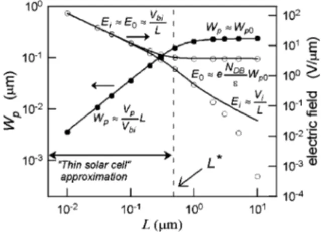
The set of equations~24! can be solved easily by itera-tive methods~although it can also be solved analytically, the general solution is not straightforward!. Figure 7 shows the dependence of the electric field profile ~i.e., the parameters E0, Ei,EL,Wp, and Wn) on the intrinsic layer thickness L for the p-i-n solar cell described in Table I. We also compare the values obtained by solving the set of equations~24! with the values extracted from the numerical results. This plot gives two different kinds of behavior, depending on whether the i layer thickness L is bigger or smaller than a critical thickness value L* related to the widths of the depletion layers in an ‘‘infinite thick solar cell:’’
L*5Wp01Wn0, ~25! with Wp05
A
2« qNDBVp and Wn05A
2« qNDB Vn. ~26!With the cell parameters listed in Table I we obtain L*
'0.5mm. At the limit of thick cells ~i.e., if L@L*), the widths of the interface regions Wp and Wn tend to Wp0 and Wn0, respectively. In this case, the electric field in the i layer departs significantly from uniformity (Ei!E0 and Ei!EL). In fact, the set of equations ~24!, where we use the zero-temperature approximation, leads to Ei'Vi/L, while nu-merical simulation shows that the electric field is much more sensitive to the i layer thickness and Eiis virtually zero. This
is a consequence of the trapped charge in the interior of the i layer, near the PI and IN regions, due to the effect of the nonzero temperature.
However, this first study focuses on the most common situation of ‘‘thin’’ solar cells~i.e., when L,L*). As can be seen in Fig. 7, in this case there is an important and nearly uniform electric field all over the i layer:
Ei'E0'EL' Vbi
L . ~27!
Note that, although in this situation the hypothesis of ‘‘uni-form field’’ is a good assumption, the charged regions ~PI and IN! in the i layer should not be neglected: the widths Wp and Wn are an important fraction of the i layer thickness. We find Wp'Vp Vbi L and Wn' Vn Vbi L. ~28!
C. Solar cell under uniform illumination
In general, when the solar cell is under external pertur-bation ~illumination or electrical bias!, the profile of charge density changes and, in consequence, the electric field profile also changes. The greatest variation in charge density occurs at the limits xp and xn of the interface regions. In the bulk of these regions the electric charge is mainly due to ionized defects and only a very high illumination level ~or applied voltage! can perturb this ‘‘fixed’’ charge. Note that in the bulk of the neutral I region, between xpand xn, the effect of the photogenerated space charge could be more important. However we assume, as a first approach, that this effect is not significant. Therefore, we will interpret the perturbation of the charge profile as the variations Dxp andDxn for the limits xp and xn of the interface regions~see Fig. 8!. As a consequence of this perturbation, the electric field will be modified by the incrementsDEp,DEi andDEn in the three regions of the cell ~note that if DQ50 in the bulk, then DE
FIG. 7. Parameters of the electric field profile in equilibrium as a function of the i layer thickness L. Solid lines are theoretical results calculated from Eq.
~24!. Data points are from numerical simulation. Note that the cell described
in Table I is symmetric so that Wp5Wnand E05EL.
is constant!. In the short-circuit condition the following rela-tionships between these increments and the variations Dxp andDxn can be found:
DEp5DEi1 qNDB « Dxp, ~29a! DEn5DEi2 qNDB « Dxn, ~29b! DEp~Wp1Dxp!1DEi~Wi2Dxp1Dxn! 1DEn~Wn2Dxn!50, ~29c!
where the first two equations in Eq. ~29! are obtained by imposing continuity of the electric field at the new limits of the interface regions, and the last equation~29c! refers to the short-circuit condition: i.e., the integral of the electric field perturbation across the i layer must be zero.
We need two more equations to calculate the variation in the electric field profile (DEp,DEi,DEn,Dxp, and Dxn). These can be obtained employing statistics. For example: note that, in thermodynamic equilibrium and using the zero-temperature approach, the limit xp was defined as the posi-tion in the i layer at which defects pass from the positive to the neutral state; i.e., Ef(xp)5E1(xp)~see Fig. 6!. Equation
~16a! shows that if TÞ0, then at xp the ratio T1for positive to neutral defects is 1/2. When the cell is under illumination, this condition will be accomplished at the new limit xp
1Dxp. So, from the more general dangling-bond statistics
@see Eqs. ~15! and ~16!#, the following conditions at the new
limits of the interface regions can be derived:
C1p~xp1Dxp!2peq~xp! n~xp1Dxp!2neq~xp! 5 C2n~xn1Dxn!2neq~xn! p~xn1Dxn!2peq~xn! 5 1 2, ~30!
where C1and C2are the ratio of capture cross sections for charged to neutral defects: C15sp0/sn1 and C25sn0/sp2.
Now, in Eq. ~30! we need to know the photogenerated carrier densities in order to solve the coupled set of Eqs.~29! and ~30!. Assuming that in the neutral region photocarrier transport occurs by field-assisted drift, and neglecting recom-bination in Eqs.~13a! and ~13b! ~see Ref. 5!, then we arrive at
Dp~x!'Gmp~L2x!E~x!
~31!
and
Dn~x!'mnGxE~x!.
As we discussed at the end of Sec. III, these expressions can be considered valid in the neutral region and valid only for minority carriers in the interface regions~electrons in the PI region and holes in the IN region!. For the majority carriers diffusion cannot be ignored and the modified field has to be borne in mind on determining the drift. However, by solving the transport equations in the absence of recombination,
simple expressions for the profiles of majority photocarriers are obtained ~see Appendix A!. So, for the PI region the result is that
Dp~x!'peq~x!
~
e2 ~DEpx/VT!21!
, ~32!where VT is the Boltzmann potential and peq(x) is the hole
profile in equilibrium which can be calculated from the elec-tric field profile in equilibrium, making jp(x)50 in Eq.
~12a!: peq~x!5peq~0!exp
F
2 x VTS
E02 qNDB 2« xDG
. ~33!Note that the illumination dependence in Eq.~32! is implicit inDEp. For photoelectrons in the IN region we arrive at a similar expression, but in the function of DEn. Now, using Eqs.~31! and ~32! in Eq. ~30! and solving the coupled set of equations~29!–~30!, we can calculate the perturbation of the electric field profile due to illumination.
In the case of thin solar cells~i.e., when the ‘‘thin solar cell’’ approximation can be applied! a useful simplification is to assume that the electric field increments can be ne-glected in comparison with the electric field value Eiin the i layer. It can be shown that this simplification enables the effect of these increments in Eq. ~32! to be removed. Thus, from Eq.~30!, we arrive at the following expressions for the thickness variationsDxp andDxn of the interface regions:
C1peq~xp!
F
expS
2 EiDxp VTD
21G
5 G mnEi~Wp1Dxp!, ~34a! C2neq~xn!F
expS
EiDxn VTD
21G
5 G mpEi~Wn2Dxn!, ~34b!where peq(xp) and neq(xn) only depend on the position of the electronic defect states:
peq~xp!5peq~0!exp
F
2 Vp VTG
5NVexpF
2 E12EV qVTG
, ~35a! neq~xn!5neq~L!expF
2Vn VTG
5NCexpF
2 EC2E2 qVTG
. ~35b!The equations forDxp andDxn in Eq.~34! are transcendent and must be solved by iterative methods. However, for low perturbation we can assume that uDxpu!Wp and uDxnu
!Wn, and then we can obtain analytical solutions forDxp andDxn. For example, ifDxp is neglected in the right term of Eq.~34a! then we arrive at
Dxp52 VT Ei ln
S
GWp C1peq~xp!mnEi 11D
. ~36!This result shows that illumination leads to a decrease in the thickness of the interface region.
D. Voltage dependence of the electric field profile
In order to evaluate short-circuit resistance, it is neces-sary to calculate the derivatives of the field profile
param-eters with respect to the applied voltage. From the electric field profile under short-circuit conditions ~i.e., E0*, Ei*, EL*, Wp*, and Wn*, where the superscript * refers to the value under illumination: e.g., Wp*5Wp1Dxp), and follow-ing an analysis similar to the one made in the previous sec-tion ~see Appendix B!, we arrive at
S
dEi* dVD
V50 5S
dE0* dVD
V50 5S
dEL* dVD
V50 52L1, ~37a!S
dWp* dVD
V505 W*p Vbi , ~37b!S
dWn* dVD
V 50 5Wn* Vbi ; ~37c!in which ‘‘thin solar cell’’ approximation is included.
E. Recombination andmtproduct
Recombination in the i layer is due to dangling bonds and depends on their charge states in the different regions. Inside the i layer ~I region! all defects can be considered as neutral and we can use the linear approximation of the re-combination function @Eq. ~1!#. In the interface PI region, where defects are positively ionized and electrons are minor-ity carriers, the recombination rate is approximately
Rpi'Dn tn1 ~38! with tn15~v thsn1NDB!21,
wheretn1 is the capture time of free electrons by positively ionized dangling bonds andsn1is the corresponding capture cross section. The analogous equation for the recombination rate in the IN region is
Rin'Dp tp2 ~39! with tp25~v ths2pNDB!21,
where tp2 is the capture time of free holes by negatively ionized dangling bonds andsp2is the corresponding capture cross section.
To calculate the total recombination Irecin the i layer, we
must take into account the contribution of the different re-gions: Irec5Irec pi1I rec i 1I rec in 5
E
0 x*pDn tn1dx1E
x p * xn*S
Dn tn0 1 Dp tp0D
dx1E
x n * LDp tp2dx, ~40!where, as mentioned earlier, Dn and Dp can be approxi-mated by Eqs. ~31! ~note that recombination in the interface regions is dependent only on the minority-carrier densities!.
Therefore, by solving the integrals in Eq. ~40! we can obtain the recombination in the different regions. In the neu-tral region integration is straightforward and gives
Ireci 5 1 mteff
~L2Wp*2Wn*!
Ei* Iph, ~41!
wheremteffis the same effectivemtproduct obtained by the
standard uniform-field model of Hubin and Shah @i.e., see Eq. ~8!!. It is important to note that at the limit of very high illumination, Wp* and Wn* can be ignored in front of L, so that the same behavior as in the standard model is found@see Eq. ~9!#.
At low illumination and, in fact, in a wide range of in-termediate illuminations, the widths of the interface regions are important and this means that recombination is deter-mined by the charged defects~with higher capture cross sec-tions than the neutral ones!. Integrating Eq. ~38! between the limits of the PI region, and using the ‘‘thin solar cell’’ ap-proximation, we arrive at
Irecpi5 1 mntn1
Wp*2
2LEi*Iph. ~42!
In the IN region a similar expression can be obtained as a function of the width Wn* and the mt product for nega-tively ionized dangling bonds (mptp2). Finally, after some manipulation, we arrive at the following expression for the total recombination in the interface regions:
Irecpi1in5Irecpi1Irecin5 1 mteff
pi1in L
Ei*Iph, ~43!
where a new effectivemt product has been introduced:
mteff
pi1in52 j
1mntn1j2mptp2
j1mntn11j2mptp2. ~44!
The coefficientsj1andj2are dimensionless and depend on the ratio of the i layer thickness L to the interface widths:
j15
S
L W*pD
2 and j25S
L Wn*D
2 . ~45!Note that j1 and j1 depend strongly on illumination. For high illumination levels these coefficients greatly increase and for low illumination levels tend to a constant value which could be evaluated from Eq. ~28! ~for ‘‘thin solar cells’’!.
Now, differentiating Eq.~43! with respect to the applied voltage @including the voltage dependence of Ei*, W*p and Wn*, from Eq. ~37!#, the short-circuit resistance can be de-duced:
Rsc'
S
dIrecpi1in dVD
V50 21 513mteff pi1in Ei*2I ph 2151 3mteff pi1inS
Vbi LD
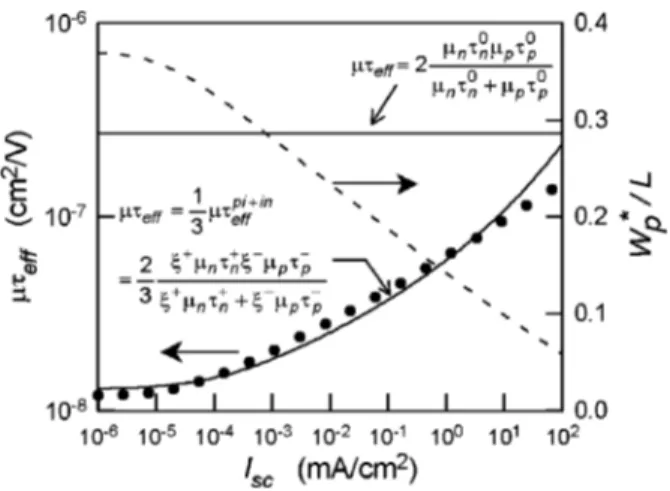
2 Iph21. ~46! This expression is similar in form to the expression normally deduced from the uniform-field model@Eq. ~10!# and, conse-quently, enables the same method to be used to analyze the variable irradiance measurement of Rsc. However, note thatthe interpretation of themt product can be very different. Figure 9 compares the numerical and analytical mt product calculations as a function of the short-circuit current Iscfor the 0.3-mm-thick solar cell with the set of parameters
given in Table I. The numericalmt product is deduced from the simulated short-circuit resistance Rsc as in Fig. 2. The
analytical mt product is separated into its two components: the bulk contribution, i.e., the standard effectivemt product given by Eq.~8! and the interface contribution given by Eq.
~44! ~to calculate the illumination dependence of the
coeffi-cientsj1andj2in Eq.~44!, we employed the most accurate relationships given by Eq.~34!!. Note that the totalmt prod-uct must be determined by the smaller of the two contribu-tions and, as we can see in Fig. 9, this is precisely the inter-face contribution.
F. Influence of surface recombination
Until now we have assumed that the contacts x50 and x5L, which define the limits of the i layer, are perfectly blocking for minority carriers: i.e., SL50 and S050 in Eq.
~21!. However, minority carriers at the contacts are usually
lost by surface recombination, and a current of the opposite sign to the active photocurrent forms. Now we examine the effect of this surface recombination on cells illuminated by uniformly absorbed light under short-circuit conditions. We focus on developing analytical expressions for the current loss at the interfaces and its dependence on voltage bias~i.e., short-circuit resistance!.
Under short-circuit conditions, the photocurrent can be obtained by subtracting the different recombination currents from the photogeneration current in the i-layer Iph:
I~V50!5Iph2Irec2Irecs , ~47! where Irecis the bulk recombination current, which has been
discussed already, and Irecs is the surface recombination, which can be expressed by the sum of the electron current at the p-i interface (x50) and the hole current at the n-i inter-face (x5L):
Irecs 5 jn~x50!1 jp~x5L!. ~48! The most simple treatment is to assume that these mi-nority currents are related to the excess of mimi-nority carriers at the interfaces according to
jn~x50!5qS0Dn~0!, ~49a!
jp~x5L!5qSLDp~L!, ~49b!
where the interface recombination velocities S0 and SL can be considered as constants.
Thus, in order to evaluate Irec
s
we need to calculate
Dn(0) and Dp(L), which can be done by solving the
trans-port equations in the regions near the interfaces. For this purpose it is useful to make some simplifying assumptions, the most obvious of which are that bulk recombination is negligible and the electric field is a constant. So, for instance, the electron photocurrent near the p-i interface (x50) can be given by
jn~x!52qmnDn~x!E01qVTmn
dDn~x!
dx , ~50!
where E0 is the absolute value of the electric field. It is important to note that, despite the focus on the transport of minority carriers, the diffusion current is not ignored in Eq.
~50!. In fact, however strong the electric field E0 may be, the
assumption of photocarrier transport by field assistance is not correct in a narrow region close to the contact x50
@note that, if x50 in Eq. ~50! this assumption leads to S0 52mnE0, which is incoherent#. In the remaining portion of
the PI region the field-assisted transport approach is valid and so this assumption can properly be a boundary condition of our problem: as we move away from the contact, diffusion becomes negligible and the minority-carrier density can be given by Eq.~31!.
Thus, using the most general expression, Eq.~50! in the continuity equation for photoelectrons, we arrive at the fol-lowing differential equation:
d2Dn dx2 2 E0 VT dDn dx 52 G mnVT . ~51!
This equation can be readily integrated, using the boundary condition thatDn(x)5Gx/mnE0 at ‘‘x→`,’’ to give
Dn~x!5Dn~0!1mGx
nE0
. ~52!
FIG. 9. mteffas a function of Isc. Solid lines are the theoretical values of
mtefffor the I region and interfaces. Dashed line shows the illumination
dependence of the width of the interface PI region deduced from Eq.~34!. Data points are the values ofmteffdeduced from numerical simulation of Rsc. (L50.3mm!.
This expression forDn(x) can be used in Eq. ~50! to deter-mine the electron photocurrent. Then, we can evaluate the electron photocurrent at x50 and, eliminating Dn(0) by means of Eq.~49a!, we arrive at
jn~0!5 VT E0 S0 ~S01mnE0! G. ~53!
For the hole photocurrent at x5L we can find a similar equa-tion but expressed in terms of SL,mp, and the absolute value EL of the electric field near x5L. Now, differentiating Eq.
~53! with respect to the applied voltage, we can deduce the
contribution of the surface recombination at x50 to the short-circuit resistance. There are two important limiting situations ~we include the ‘‘thin solar cell’’ approximation, i.e., E0'Ei'Vbi/L):
~A! Weak surface recombination (S0!mnEi): Irecs 5VT Vbi2 S0 mnLIph, ~54a! Rsc5 Vbi3 2VT mn S0 L21Iph21. ~54b!
~B! Strong surface recombination (S0@mnEi): Irecs 5VT Vbi Iph, ~55a! Rsc5 Vbi2 VT Iph21. ~55b!
A significant aspect of these results is the dependence of Rscon the i layer thickness L: for weak surface
recombina-tion, Rsc is proportional to L21 and, for strong surface
re-combination, Rscis independent of L. This behavior is dif-ferent from what is found in the case of bulk recombination, in which Rsc, derived from the voltage dependence of re-combination in both neutral and interface regions, is propor-tional to L22.
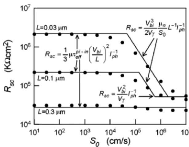
In order to examine the effect of the surface recombina-tion , and to check the validity of Eqs.~54! and ~55!, Fig. 10 shows plots of the numerical and analytical Rsccalculations
as a function of S0for solar cells with different i-layer
thick-ness~the remaining cell parameters are given in Table I!. We consider uniform illumination with Iph51023mA/cm2.
Fig-ure 10 shows that Rscis only determined by surface
recom-bination in the case of very thin solar cells (L,0.3mm!, and at sufficiently high S0 (.104 cm/s!.
V. SUMMARY
Our numerical simulation results reproduce the experi-mental data of the illumination dependence of the short-circuit resistance Rscin a-Si:H p-i-n solar cells. These re-sults suggest that recombination in the charged regions of the i layer should not be overlooked. We then developed a new analytical model to describe collection in p-i-n structures under short-circuit conditions and uniform illumination. The recombination current and the short-circuit resistance can be given as a function of a mt product which adequately com-bines two effective mt products for the different regions in
the i layer:~1! for the neutral region in the bulk of the i layer we find the same effectivemtproduct as is obtained with the standard uniform-field model, ~2! for the charged regions at the interfaces we find a new effective mt product which is light-dependent. We show that recombination and Rsc are
determined by this lattermtproduct in a wide range of illu-mination.
We also examined the effect of surface recombination. We demonstrated that, under uniform illumination and short-circuit conditions, surface recombination could not be negli-gible in very thin solar cells at sufficiently high surface re-combination rates. It could be evaluated by a check on the effect of the i-layer thickness on Rsc.
We have also shown that, in the analysis of p-i-n solar cells, it is necessary to take into consideration both the dif-fusion process for majority carriers at interfaces and the ef-fect of the variation in the electric field. We obtained el-ementary expressions that can be used in analyzing the general behavior of p-i-n solar cells.
ACKNOWLEDGMENTS
The authors thank Professor A. V. Shah for valuable discussions. This study was supported by the CRYSTAL program of the EC~Grant No. JOR3-CT97-0126!.
APPENDIX A: MAJORITY-CARRIER PROFILES IN SHORT-CIRCUIT CONDITIONS
In the interface regions near the doped layers, the majority-carrier densities and the gradients are important: carrier diffusion from the doped regions cannot be ignored in determining the transport and. moreover, the electric field variation DE caused by illumination can also contribute to the photocurrent. Thus, in the PI region the hole photocur-rent, expressed in terms of increments, should be given by
FIG. 10. Short-circuit resistance as a function of the surface recombination rate S0for solar cells with different i layer thickness. It is considered that Iph51023 mA/cm2. Solid lines are the theoretical values of R
sc~the main
contribution is plotted! and data points are the values of Rscobtained from
numerical simulation.~We assume that the contact x5L is perfectly block-ing.!
jp~x!/q52mppeq~x!DEp2mp@Eeq~x!1DEp#Dp~x!
2mpVT dDp
dx , ~A1!
where peq(x) is the hole density profile in equilibrium@given by Eq.~33!#, Eeq(x) is the electric field profile in equilibrium
@note that it is positive, see Eq. ~22!#, and DEp is the electric field variation in the PI region due to illumination. As has been discussed, the photogenerated space charge in the bulk of the PI region is negligible, and so it can be assumed that
DEp is a constant. Thus, introducing Eq.~A1! into the con-tinuity equation, and ignoring recombination, we find the following differential equation for the hole density increment in the PI region: d2Dp dx2 1 1 VT@Eeq~x!1DEp# dDp dx 2 1 VT qNDB « Dp 52 G VTmp 2DEp VT d peq dx . ~A2!
This equation can be solved for Dp and gives a relatively complicated expression which is expressed in terms of the error function Erf(y ). It can be demonstrated that this func-tion is well approximated by 12e2y2/
A
py and, using the boundary condition thatDp(x50)50 ~ i.e., assuming ohmic contact!, after some manipulation we arrive atDp~x!5peq~x!
F
~12C!expS
2 DEpx VTD
21G
1mppeq~0!~E01DEp!C2Gx mp@Eeq~x!1DEp# , ~A3!where C is the constant of integration that we should obtain by imposing a new condition. To this effect, from Eq.~A3! we can calculate the hole photocurrent in the PI region. It can be demonstrated that only the drift component of the second term on the right-hand side of Eq.~A3! significantly contrib-utes to the photocurrent~the first term gives a diffusion com-ponent that is compensated by drift!. The result is that
jp~x!/q'Gx2mppeq~0!~E01DEp!C. ~A4! On the other hand, from the continuity equation for holes, neglecting recombination and imposing jp(L)50, we find
jp~x!/q52G~x2L!, ~A5!
then, equating Eqs. ~A4! and ~A5! we can determine the value of C:
C5 GL
mppeq~0!~E01DEp!
. ~A6!
For a typical solar cell ~defined by the set of parameters given in Table I! under high illumination (Iph510 mA/cm2)
we find C'1024, so that C!1, and so this constant can be safely ignored in the first term of Eq.~A3!. Finally, substi-tution of Eq.~A6! into Eq. ~A3! yields
Dp~x!5peq~x!
F
expS
2 DEpx VTD
21G
1mp~E G eq~x!1DEp! ~ L2x! ~A7!Note that the second term in Eq.~A7! is the photogenerated hole distribution that we obtain making the field-assisted drift assumption @see Eq. ~31!# and, as we have seen from Fig. 5, this is only a very small fraction of the total. We thus obtain the relationship given by Eq.~32! for the photogener-ated hole profile in the PI region.
APPENDIX B: EFFECT OF APPLIED VOLTAGE „DERIVATIVES…
We examined a p-i-n solar cell in short-circuit condi-tions under weakly absorbed light. Illumination alters the electric field profile by the incrementsDxp,Dxn,DEp,DEi, and DEn, so that the analytical expressions for the profiles of electric field and carrier densities are:
~A! PI region (0,x,Wp*): E*~x!5E0*2qNDB « x, ~B1a! p*~x!'peq~0!exp
F
2 x VTS
E0*2qNDB 2« xDG
, ~B1b! n*~x!' Gx mnE*~x! . ~B1c! ~B! I region (Wp*,x,Wn*): E*~x!5Ei*, ~B2a! p*~x!'G~L2x! mpEi* , ~B2b! n*~x!' Gx mnEi* . ~B2c! ~C! IN region (Wn*,x,L): E*~x!5EL*2qNDB « ~L2x!, ~B3a! p*~x!'G~L2x! mpE*~x!, ~B3b! n*~x!'neq~L!expF
2 ~L2x! VTS
EL*2qNDB 2« ~L2x!DG
. ~B3c!The superscript*in Eqs.~B1!–~B3! refers to the value under illumination. In this situation, if a small external voltage V is applied, then the electric profile will change. The widths Wp* and Wn* will be modified by the new increments Dxvp and
Dxn
v, respectively, and, assuming that the variation of the
space charge in the bulk of the different regions is negligible, the electric field will be modified by the constants DEvp,
DEiv, andDEnv. Using an argument similar to the one in Sec. III C, we find the following relationship among these incre-ments: DEp v5DE i v1qNDB « Dxp v, ~B4a! DEn v5DE i v2qNDB « Dxn v, ~B4b! DEp vW p *1DEivWi*1DEnvWn*52V; ~B4c!
where, in the last equation~B4c!, we assume that the applied voltage is sufficiently small for uDxpvu!Wp* and uDxnvu
!Wn*. The two remaining equations can be obtained, as in Sec. III C, by imposing T1(xp*1Dxpv)51/2 and T2(x
n
*
1Dxn
v)51/2 @i.e., Eq. ~30!#.
On the other hand, if low applied voltage is assumed, it can be demonstrated that the most significant perturbation of carrier distribution occurs for majority carriers in the inter-face regions. To obtain the hole profile in the PI region, we can reach a differential equation similar to Eq.~A2! but for the hole density increment due to the electrical bias. Thus, solving the differential equation, we find that the total hole density in the PI region is well approximated by
p~x!'p*~x!exp
F
2DEpv
VT
x
G
, ~B5!where p*(x) is the hole distribution in the PI region for the cell in short-circuit conditions under illumination. Now, in-troducing Eq. ~B5! in the condition T1(xp*1Dxpv)51/2 we
arrive at p*~xp*!exp
F
2 1 VT~Ei *Dxvp1xp*DEvp!G
' GWp* mnEi*C11peq~xp!, ~B6!where the second term could be considered a constant. So, differentiating Eq.~B6! with respect to V we obtain
dDxvp dV 52 Wp* Ei* dDEpv dV . ~B7!
From this equation and differentiating Eq.~B4a!, we arrive at the following relationship between the derivatives of Ep*and Ei*:
S
dEp* dVD
V50 5Ei* E0*S
dEi* dVD
V50 . ~B8!Using similar reasoning in the IN region, we could arrive at
S
dEn* dVD
V50 5Ei* EL*S
dEi* dVD
V50 . ~B9!It now remains to calculate the derivative of Ei* with respect to V. This can be done by differentiating Eq. ~B4c! and using Eqs. ~B8! and ~B9!. We find
S
dEi* dVD
V50 52S
Ei* E0*Wp*1Wi*1 Ei* EL*Wn*D
21 . ~B10! For ‘‘thin’’ solar cells, it can be shown that this last derivative reduces to 21/L. Also, for high illumination lev-els, when the neutral I region fills the i layer, the derivative of Ei* tends to21/L.Other useful relationships are the derivatives of Wp*and Wn*with respect to V. These can be most easily expressed as a function of the derivative of Ei*
S
dWp* dVD
V50 52W*p E0*S
dEi* dVD
V50 , ~B11a!S
dWn* dVD
V5052 Wn* EL*S
dEi* dVD
V50. ~B11b! 1M. Hack and M. Shur, J. Appl. Phys. 58, 997~1985!.2J. L. Gray, IEEE Trans. Electron Devices ED-36, 906~1989!. 3
J. M. Asensi, J. Andreu, J. Puigdollers, J. Bertomeu, and J. C. Delgado, Mater. Res. Soc. Symp. Proc. 297, 315~1993!.
4R. S. Crandall, J. Appl. Phys. 54, 7176~1983!.
5J. Hubin and A. V. Shah, Philos. Mag. B 72, 589~1995!.
6J. Merten, J. M. Asensi, C. Voz, A. V. Shah, R. Platz, and J. Andreu,
IEEE Trans. Electron Devices ED-45, 423~1998!.
7S. S. Hegedus, Prog. Photovolt. Res. Appl. 5, 151~1997!.
8J. Hubin, A. V. Shah, and E. Auvain, Philos. Mag. Lett. 66, 115~1992!. 9A. V. Shah, J. Hubin, E. Sauvain, P. Pipoz, N. Beck, and N. Wyrsch, J.