Laser integration on
Silicon-on-Insulator platform
Tommaso Cassese
Supervisor: Dr. Giampiero Contestabile
Tutor: Marco Romagnoli
TECIP Institute
Sant’Anna
School of Advanced Studies - Pisa
This dissertation is submitted for the degree of
Doctor of Philosophy
Acknowledgements
Il mio grazie più grande va a Zaira. Non hai mai smesso di supportarmi durante tutti questi anni. Ogni volta che mi sono messo alla prova lei c’era e credeva in me. Mi ha sempre spinto a migliorare e so che continuerà a farlo. Grazie!
A Vito Sorianello va invece un altro ringraziamento speciale. Non è stato per me solo un collega ma un fidato amico. Molto di quello che ho ottenuto lo devo a lui e al tempo che ha dedicato alla mia crescita come ingegnere e ricercatore. Grazie a Valentina e anche alla piccola Diana. Voi siete stati i miei più saldi riferimenti fin dall’inizio.
Grazie a Marco Romagnoli, mi ha sempre spinto al limite sapendo che ne avrei giovato. Grazie per la tua lungimiranza e per tutti i preziosi consigli, ne farò buon uso.
Grazie ai miei relatori, Dr. Giampiero Contestabile e Prof. Giancarlo Prati. La vostra fiducia nelle mia capacità è stata per me fondamentale. Senza il vostro supporto non avrei potuto fare le esperienze che hanno dato così tanto a me e al mio dottorato.
Grazie al gruppo Inphotec: Alessandro, Davide, Fabio, Francesca, Gianni, Karol, Marco, Sergio, Stefano, Stefano, Veronica. Vi devo molto, il vostro duro lavoro è alla base di molti dei risultati riportati in questa tesi. Tutti voi avete creduto in me e mi avete accolto a braccia aperte nella vostra grande famiglia. Se come dice Sergio, la tecnologia è dura come scalare una montagna, io sono contentissimo di aver chiuso così tanti tiri con voi. Grazie a tutti i componenti del Sant’Anna e del CNIT che mi hanno aiutato anche solo con un sincero saluto al mattino.
Many thanks to Prof. Dries Van Thourhout and Prof. Gunther Roelkens for accepting me in UGent research group. Thank to you I had an experience that I will hardly forget. I want to especially thank Joan Juvert, Sarah Uvin and Andreas De Groote. They started the work on transfer printing and I had the honour of working with them in the development of this technology. Joan definitely deserve deserve a prize, his patience was daily challenged and never broke. Thanks to the people that, even knowing I was about to get "rotten" in few months, demonstrated sincere friendship from the beginning. So thanks to Ali, Alejandro, Amin, Andrew, Jesper, Jing, Leili, Mahmoud, Mattias, Nina, Paul, Sanja, and to my fellow Italians Alessio, Fabio and Paolo.
iv
A Paolo Carai ho tanto da ringraziare. Da quando ti ho conosciuto ti ho solo visto sorridere e questo mi ha sempre dato una grande energia. Grazie per il fantastico tempo passato insieme.
Grazie a Stefano Petrangeli, sei stato il pezzo d’Italia in Belgio che mi serviva. Grazie a Giulia per le intense chiacchierate. Grazie a Donato, amico onnipresente. Grazie ai casa Barsotti: Andrea, Valentino e Vincenzo. Grazie ai suanderful per tutti gli assommi e quelli che verranno: Azzurra, Chiara, Daniela, Giorgio, Isadora, Michele, Olga, Simone.
Grazie a mio fratello Alessio e a mia sorella Nicole. Ne abbiato passate tante in questi tre anni, ma il nostro rapporto è più forte che mai e saremo sempre presenti l’uno per l’altro.
Ai miei genitori, grazie a voi so che è importante non arrendersi mai e continuare a crederci sempre.
Grazie a Floriano per i pranzi passati a parlare di fisica abbracciati ad una bottiglia di plastica. Grazie a Giusy e Michele per il loro affetto.
Grazie a tutti coloro che anche per un solo istante mi hanno aiutato. Questa tesi è frutto non solo del mio impegno, ma di un enorme lavoro di gruppo in cui ognuno ha avuto il proprio ruolo sempre fondamentale.
Abstract
Silicon photonics (SiPh) is defined as the application in photonics of silicon as optical medium. Using this technology a large group of devices has been developed and already put on the market. Silicon-on-Insulator (SOI) is one of the most used platforms for the development of SiPh devices. The crucial advantage of SOI is that its fabrication processes are CMOS compatible. On the other hand, silicon indirect bandgap properties hamper the achievement of an electrically pumped laser fabricated on chip and made of this material.
In order to overcome this limit several approaches have been proposed. A laser chip can be coupled with a SiPh integrated circuit (IC) by using a set of lenses that focuses the beam emitted by the laser on the circuit input coupler. Unfortunately, this approach has a high fabrication cost per chip and it is not power efficient. A second solution consists of bonding a stack of III-V layers on the top silicon of the SOI wafer. By properly processing the III-V stack it is possible to fabricate a laser directly on top of a silicon waveguide. Since there is no need of lenses for coupling, the fabrication cost is lower in this case than in the previous one. But using this solution the laser will be fabricated on top of a thick dielectric layer that would impede the dissipation of the laser heat towards the silicon substrate. This could limit the lifespan of the device itself.
In this work we developed and compared two novel approaches for the SiPh source integration issue. The first one, developed in Scuola Superiore Sant’Anna, exploits a flip-chip bonding technique. The second one has been developed in collaboration with the Photonics Research Group of the University of Ghent. It exploits a new technique called "transfer printing". In both cases the active device is bonded in direct contact with the silicon substrate in order to improve thermal dissipation. The light sources are fabricated before being transferred on the fully processed SOI. Both bonding processes are wafer scalable.
In the flip-chip approach we developed a novel and high efficient edge coupler that is used for coupling between the active device and the SOI circuit. The edge coupler was fabricated and tested obtaining coupling loss as low as 0.7dB. The same coupler has been used also for demonstrating an external cavity laser. This fabricated laser had a low threshold current of 8mA and a high maximum power of 5mW emitted in silicon waveguide. We designed
vi
and developed as well the processing of the SOI wafer, devoting particular attention to the deposition of the gold-tin solder alloy used for the device bonding.
For the integration process employing the transfer printing technique we designed and developed the fabrication process of both the III-V light source and the SOI circuit. Final test of the device showed emission at the SOI circuit output. This was the first electrically pumped III-V source butt-coupled with a silicon waveguide fabricated using this technique.
Table of contents
List of figures ix
List of tables xiii
Nomenclature xv
1 Introduction 1
1.1 Outline . . . 1
1.2 Background . . . 1
1.3 Photonics platforms . . . 3
1.4 III-V integration on SOI . . . 7
1.5 Developed integration processes . . . 9
1.5.1 Integration by flip-chip bonding . . . 9
1.5.2 Integration by transfer printing . . . 10
2 III-V/SOI edge coupling 13 2.1 State of the art . . . 13
2.2 The "kite" edge coupler . . . 16
2.2.1 Butt coupling optimization . . . 18
2.2.2 Spot size converter optimization . . . 22
2.2.3 Edge coupler fabrication . . . 26
2.2.4 Testing . . . 29
2.3 Conclusions . . . 33
3 Integration by flip-chip bonding 35 3.1 Introduction . . . 35
3.2 SOA design . . . 37
3.3 SOI PIC design and fabrication . . . 41
viii Table of contents
3.5 Conclusions . . . 46
4 Integration by transfer printing 49 4.1 Introduction to transfer printing . . . 49
4.2 Fundamentals of transfer printing . . . 51
4.3 SOI circuit: design and processing . . . 54
4.4 III-V device: design and processing . . . 58
4.4.1 Design and simulation results . . . 60
4.4.2 Processing . . . 62
4.5 Coupon transfer printing and post processing . . . 67
4.6 Device testing . . . 69
4.7 Conclusions . . . 71
5 Tunable laser design, fabrication and characterization 73 5.1 State of the art . . . 73
5.2 Cavity design . . . 75
5.2.1 Bragg reflector design . . . 77
5.2.2 Ring filter design . . . 78
5.3 ECL fabrication, packaging and testing . . . 81
5.3.1 Fabrication . . . 81
5.3.2 Packaging . . . 81
5.3.3 Testing . . . 83
5.4 Conclusions . . . 84
6 Conclusions and perspective work 87 6.1 Conclusions . . . 87
6.2 Perspective work . . . 89
List of publications 91
List of figures
1.1 Evolution of data traffic per month from 1984 to 2014 [1]. . . 2 1.2 Volumes of connections in relation to the transmitter-receiver distance . . . 3 1.3 Section view of the integrated III-V stack bonded over the silicon layer [2]. 7 1.4 (a) Schematic view of the laser cavity with the III-V material bonded on the
silicon surface and (b) a detail of the coupling region between silicon and III-V waveguide [3]. . . 8 1.5 Schematic view of the approach adopted by Skorpios [4]. . . 9 1.6 A schematic view of the SOA integration process developed for Inphotec
processing. In detail is shown the coupling between the SOA and the SOI waveguide through the designed EC. . . 10 1.7 A schematic view of the LD integrated on SOI by mean of transfer printing. 11 2.1 (a)Schemtaic view of the LD integration approach and (b) detail of proposed
EC [5]. . . 14 2.2 Coupling loss versus (a) horizontal misalignment and (b) vertical
misalign-ment [5]. . . 15 2.3 (a) Structure of trident on SOI wafer; (b) calculation results for mode
mis-match loss and design of structure of trident EC [6]. . . 15 2.4 Measured value of coupling loss moving the LD source both in the vertical
and horizontal direction [6]. . . 16 2.5 Refractive index of Si3N4deposited with LPCVD on silicon substrate. . . . 18
2.6 View of the SOA waveguide and dimensions detail. . . 19 2.7 View of the coupling region between the SOA core and the SiN core on the
SOI chip. . . 19 2.8 TE0mode electric field intensity profile of the SOA waveguide when
x List of figures 2.9 (a) coupling loss versus width (b) and thickness of Si3N4 core. In (c) the
simulated structure with optimal width and thickness value. In (d) the electric field intensity profile of the fundamental TE mode. . . 21 2.10 Overlap integral between SOI EC mode and SOA beam versus horizontal
(blue line) and vertical (red line) deviation. . . 22 2.11 Structure of the EC with detailed dimensions and EC section view. . . 23 2.12 Coupling loss depending on silicon inverse taper length. The Si3N4structure
is adapted to the taper length. . . 24 2.13 (a) Normalized Poynting vector simulated value in a x-z plane cut of the EC.
(b) Normalized Poyting vector simulated value in a y-z plane cut of the EC. 25 2.14 Coupling loss depending on distance between the SOA and the SOI facet.
The Si3N4core of the EC is 1µm far from the SOI facet. . . 26
2.15 Sequence of process steps for silicon waveguide fabrication. . . 27 2.16 SEM picture of the fabricated Si inverse taper part of the EC structure. . . . 28 2.17 Sequence of process steps for EC fabrication. . . 28 2.18 (a) EC loss test structures and (b) and detail of two facing EC separated by
1µm. . . 30 2.19 (a) Setup for EC to tapered fiber coupling loss and (b) coupling loss values
with fiber vertically (red curve) and horizontally (blue curve) misaligned. . 31 2.20 (a) RSOA mounted on a silicon substrate and (b) packaged RSOA-SOI chip
with fiber array attached. . . 32 2.21 (a) Setup for the back-to-back loss and (b) setup for measuring the
RSOA-SOI coupling loss. . . 32 3.1 (a) SOA and photonic substrate integration test vehicle. (b) Fiber-to-fiber
gain vs wavelength for all 4 channels [7]. . . 37 3.2 (a)Schematic representation of the flip-chip integration approach by Aachen
University. (b) LI curve of the flip-chip integrated laser (black line) and LI curve of an identical laser mounted over a ceramic substrate (red line). Measurements done with laser at 20°C [8]. . . 38 3.3 Schematic representation of the SOA chip before bonding. . . 38 3.4 Schematic lateral view of the SOA (shades of purple) integrated on SOI. The
figure is not in scale. . . 39 3.5 Microscope pictures of the SOA. (a) full SOA top view with visible p and
n contacts and central waveguide. Close-up picture of the SOA output waveguide (b) and alignment marker (c). . . 40 3.6 Schematic top view of the SOI chip prior to integration. . . 41
List of figures xi
3.7 SEM picture of the trench fabricated in a test run. . . 42
3.8 Fabrication process steps from the BOX etching (b) to the solder deposition (e). 43 3.9 Top view of a test run with completed trench and metal deposited. . . 44
3.10 Au-Sn binary phase diagram. . . 45
3.11 Picture of a 6" silicon wafer with solder pads fabricated by evaporation. . . 45
3.12 XRF analysis results. . . 46
3.13 Silicon dummy sample bonded and then detached from a stripe of solder deposited on a 6" silicon wafer. . . 47
4.1 Schematic view of TP process. (a) The objects on the source substrate (b) are picked up by an elastomeric stamp, (c) transferred on the target substrate and (d) printed [9]. . . 50
4.2 Results of the roll test shown in [10]. . . 52
4.3 Stamp separation energy vs stamp detachment speed and critical velocities for picking and printing. . . 53
4.4 Single test structure for T sources. . . 54
4.5 Sequence of process steps on SOI wafer made in IMEC fab. . . 56
4.6 Sequence of process steps on SOI chip made in UGhent clean room. . . 57
4.7 (a) Example structure of the trident input and (b) simulated fundamental TE mode of this structure. . . 60
4.8 (a) Coupon waveguide structure and (b) its simulated fundamental TE mode. 61 4.9 Top view of the coupling area between the III-V coupon and the SOI SSC. In detail the distances between the facets. . . 62
4.10 Coupon processing steps from native chip (a) to released coupon (h). . . 62
4.11 SEM pictures of a test etch on InP dummy sample. . . 64
4.12 N-contacts deposited on sample before sacrificial layer etch. . . 65
4.13 Microscope top view of the encapsulated coupon. . . 66
4.14 Picture of the InP sample once the release process is terminated and prior to TP. 67 4.15 Picture of the SOI sample after coupons TP. . . 68
4.16 Post process steps for contact pads fabrication. . . 69
4.17 Top view of the printed coupon as the integration process is completed. . . 70
4.18 LIV curves of the tested 700µm long coupon. Solid lines for the measure-ments with the SOI chip at 5°C, dotted lines for 20°C. . . 71
4.19 OSA measured emission spectrum of integrated coupon for different bias current values: 20mA black line, 40mA red line and 90mA blue line. . . 72
xii List of figures 5.1 (a) Setup of the ECL measurement. (b) Picture of the RSOA aligned with
the SOI chip. (c) SEM picture of the Bragg reflector fabricated in the silicon
layer [11]. . . 74
5.2 Setup of the ECL measurement showint the SOA coupled with the SOI chip where a wavelength tunable filter is fabricated [12]. . . 75
5.3 ECL schematic structure. . . 76
5.4 (a) DBR reflectivity power vs length; (b) reflectivity spectrum of the 3µm long DBR. . . 78
5.5 (a) ring resonator add-drop structure [40]; (b) through (red line) and drop (blue line) port transmission spectrum. . . 79
5.6 The black line represent the superposition of the ring drop transmission spectrum (blu line) on the cavity transmission spectrum (red line). . . 80
5.7 Top view of the fabricated PIC used for the ECL experiment. . . 82
5.8 The active RSOA alignment setup. . . 83
5.9 Picture of the final ECL assembly. . . 83
5.10 LIV curves of the ECL. . . 84
5.11 Emission spectrum measured with an optical spectrum analyser at different substrate temperature. . . 85
List of tables
2.1 SSC insertion loss measurement . . . 29
2.2 RSOA gain at λOP= 1550nm . . . 33
4.1 Epitaxial layer stack . . . 59
Nomenclature
Acronyms / Abbreviations AlOx Aluminum Oxyde AR Anti-reflection
ARPANET Advanced Research Projects Agency Network AuSn Gold-tin
BCB Benzocyclobutene BOX Buried oxide
BPM Beam propagation method DBR Distributed Bragg reflector DFB Distributed feedback EC Edge coupler
ECL External avity laser
EDFA Erbium doped fiber amplifier FDTD Finite difference time domain FSR Free spectral range
FWHM Full width half maximum GC Grating coupler
xvi Nomenclature HR High reflectivity
I/O Input / Output
ICP-RIE Inductively coupled plasma - Reactive ion etching IL Insertion loss
InP Indium phosphide IT Information technology LD Laser diode
LED Light emitting diode LN Lithium niobate
LPCVD Low pressure chemical vapour deposition MFD Mode field diameter
MFW Mode field width MQW Multi-quantum well MTTF Mean time to failure PC Personal computer PDK Process design kit PDMS Polydimethylsiloxane PD Photodetectors
PECVD Plasma enhanced chemical vapour deposition PIC Photonic integrated circuit
PR Photoresist
PSR Polarization splitter and rotator RF Radio frequency
Nomenclature xvii SAC Sacrificial
SEM Scanning electron microscope SiO:Ge Germanium doped silica Si3N4 Silicon nitride
SiO2 Silicon dioxide
SiON Silicon oxynitride SiOx Silicon enriched oxide SiPh Silicon photonics SMF Single mode fiber
SMSR Side mode suppression ratio SOA Semiconductor optical amplifier SOI Silicon on insulator
SSC Spot size converter TEC Thermoelectric cooler TEOS Tetraethyl orthosilicate TE Transverse electric TP Transfer printing UV Ultraviolet
WDM Wavelength division multiplexing WPE Wall plug efficiency
Chapter 1
Introduction
1.1
Outline
This work consists of six chapters. This chapter discusses the role of photonics in contem-porary information technology, it reports some of the photonics platforms available and introduces the concept of heterogeneous integration. A brief introduction to our integration approach is reported as well. Chapter 2 is dedicated to the detailed description of the EC used for efficiently coupling light to and from the SOA chip. It reports the entire flow of design, fabrication and testing. Chapter 3 shows the process steps for achieving integration by flip-chip bonding highlighting the design choices made in order to maximize coupling efficiency and heat dissipation. In Chapter 4 the focus is the TP integration process, going from design of PICs and fabrication processes, to final test. Chapter 5 is dedicated to the design, fabrication and testing analysis of an external cavity laser fabricated and packaged in InPhoTec labs. Conclusions and further analysis are discussed at last in Chapter 6.
1.2
Background
Starting with the introduction of the Advanced Research Projects Agency Network (ARPANET) in 1969, information technology (IT) has had a sensible impact on our daily life [13]. Through the years it completely revolutionised the way people exchange information: today billions of persons are using the internet to make calls, send messages, read news, watch media contents, check their bank account and make all sort of transactions. In 2017, every minute, Amazon sold products for 258’751.90$, Google conducted 3’607’080 searches and YouTube users watched 4’146’600 videos [14].
2 Introduction All these information travelling around the globe are generating an increase in data traffic over the network. In June 2017 CISCO reported in its annual Cisco Visual Networking Index forecast historical data and traffic projection from present days to 2021 [15]. In Fig. 1.1 are reported the amounts of data in Exabyte (EB) per month (where 1EB is equal to 1 billion Gigabytes) transmitted over the network from 1984 to 2014. While in 1984, 15 years after the introduction of ARPANET, there were transmitted only 15 GB/mo, in 2014 42 EB/mo were travelling through the network: more than 1 billion times bigger than the ’84 value.
Fig. 1.1 Evolution of data traffic per month from 1984 to 2014 [1].
Cisco reports as well that the annual global IP traffic will reach 3.3 ZB/year (ZB = 1000 EB) by 2021, while in 2016 it was 1.2 ZB/year. In 2016 wired devices accounted for the majority of IP traffic, about 51% of the total. By 2021 instead, traffic from wireless and mobile devices will account for more than 63% of total IP traffic. These numbers are depicting the world of communication as something that continuously change and seeks innovation.
At the beginning of the XX century all communications were running on bulky metallic cable or through noisy radio connections. A network based on this technology would be simply incapable of supporting all the data travelling on the network nowadays, as well as in the future. What is keeping the door open to the huge growth of data transfer forecast by CISCO is the continuous evolution of photonics technologies.
1.3 Photonics platforms 3
1.3
Photonics platforms
Photonics became popular when optical fibers began to be adopted as a medium for data transmission. With this technology it was possible to reach, for the first time, high data rate over long distances with small loss per kilometre [16]. Fig. 1.2 shows the connections volumes in the network depending on the distance between transmitter and receiver. The number increases as the distance shortens. In this figure it is is also highlighted that photonics has already replaced copper in long haul and rack-to-rack communication links. In the coming years, by exploiting optical interconnects in board-to-board and chip-to-chip ones, the volumes of photonics device in the network could exponentially grow.
Fig. 1.2 Volumes of connections in relation to the transmitter-receiver distance Photonics nowadays is not only employed in telecommunication and datacom. Sensing, RF processing and computing are just some examples of the application fields benefiting from the advantages of this technology. Contemporary photonics relies also on a vast collection of devices. The materials of which these devices are made of depends on the application they will serve.
Lithium niobate (LN), for example, is a ferroelectric material with excellent electro-optic and piezoelectric properties. It is largely used for optical modulation and Q-switching in infrared wavelength range [17]. Fast electro-optic modulation has been developed in on-chip LN waveguides formed by proton exchange or titanium diffusion techniques [18, 19].
4 Introduction Furthermore LN high volume production has been achieved and fabrication techniques are well developed [20]. However, LN devices are often too bulky, making its footprint too large compared to other technologies, especially now that photonics is experiencing a fast acceleration towards integration of different capabilities on the same Photonic Integrated Circuit (PIC).
III-V materials instead, are usually employed in the fabrication of light sources or amplifiers, but they can serve a variety of other applications. Indium Phosphide (InP) is one of the most developed and commercialized platform. Both active and passive devices, operating at different wavelengths, can be integrated on this platform [21]. InP has been largely adopted in telecom applications, e.g. high efficiency transceiver [22] or fast wavelength switching [23], in the RF signal processing e.g. comb generation [24] and in sensing [25]. But on the other hand III-V platforms come with some disadvantages. In order to have passive components integrated with active ones on the same chip e.g. phase modulators and lasers, it is necessary to properly engineer the material bandgap over the wafer surface so that passives do not suffer high losses. This requires to implement critical processes e.g. crystal regrowth, just to overcome this particular issue. On top of that, InP platform has a fabrication cost per chip that is higher compared to other platforms, and it struggles to reach the high volume production required by the electronics market [26].
Silicon photonics (SiPh) is defined as the application in photonics of silicon as optical medium. Silicon is the second most abundant element on Earth crust, after oxygen [27], and it is already largely used in the electronics industry. Without it IT would not be the same: microelectronics and computing completely rely on silicon, each processor installed in our PC, smartphone or car is made out of this material. The fact that it already exists a vast knowledge of how to efficiently fabricate massive amounts of silicon devices containing millions of small features, is making SiPh really attracting in the market. Furthermore, SiPh processing exploits the same fabrication processes used and developed in standard complementary metal-oxide-semiconductor (CMOS) fabrication. This means that it is possible to fabricate PICs and microelectronics in the same fab or even on the same chip. It is also expected that SiPh would be the technological solution enabling the deeper electronic-photonics integration required to achieve optical link implementation at lower levels i.e. board-to-board and chip-to-chip [28, 29].
The most used platform for SiPh technology development is the Silicon-on-Insulator (SOI) one. In this platform the wafers are made of a thin layer of silicon, typically 220 nm thick, over a 2µm, or 3µm, thick dielectric layer made out silicon dioxide. This stack is laying over a thick silicon substrate. Choosing SOI wafers (with different buried oxide layer thickness) is not usual in electronics since the dielectric layer limits the heat dissipation from
1.3 Photonics platforms 5 the transistors to the substrate, but this layer is fundamental for SiPh in order to create the perfect condition for light propagation in circuits.
On this platform it has been already demonstrated the possibility to fabricate numerous components that are making SiPh a viable option for telecom, sensing or RF processing applications. They all tend to satisfy three main requirements:
• to introduce low optical loss, reducing energy per bit requirement and, consequently, transceiver operational power;
• to be fast, so that SiPh is capable of keeping up with the growing volumes of data travelling between boards and chips;
• to have small footprint. PICs chip size is comparable with the electronics one.
Major attention has been devoted on finding efficient solutions for light input/output (I/O) from silicon PICs. Grating couplers and edge couplers are the most used nowadays. Grating couplers (GC) are components working on the principles of Bragg’s law and they are used to couple two out-of-plane beams. In the case of SiPh the light incident on the grating is coupled with the mode propagating in the silicon waveguide. There are many examples of GC designs, with insertion loss that can be as low as 0.68 dB [30]; but achieving such performances requires really complex fabrication processes. GC insertion loss is also wavelength dependent, typical 3dB bandwidth is around 60nm [31]. GC are often designed to accept a single polarization (usually TE), meaning that in order to maximize the coupling efficiency the polarization of the incoming light has to be precisely controlled. There are also GC designs capable of accepting every polarization state at the input. The example in [32] consists of a grating with two output waveguides, depending on the incoming polarization, the input power is splitted between the two outputs in two distinct TE modes. There are ways of overcoming this issue and efficiently recombine all the light in a single output waveguide as reported in [33].
Edge couplers (EC) are used for I/O as well, but they couple two in-plane beams: generally the one coming from the fiber is coupled with the one propagating in the silicon waveguide or vice versa. ECs could be really efficient with a flat and large bandwidth. There are several examples of ECs in literature [34–38, 5, 6]. Each of these have been designed optimizing the coupling between a silicon waveguide and various types of input fields. ECs are typically polarization insensitive. This means that input beams with any state of polarization are coupled into the silicon waveguide. This property of the ECs could be a limit if the PIC is designed to operate with a single state of polarization. There are solutions to overcome this problem like using polarization splitter and rotators (PSR) [39], but till now not all fab have it available on their PDK.
6 Introduction Filters, modulators and photodetectors have also been developed. In SiPh there are many solutions for filter design. Probably the most employed ones are the ring resonators [40], they are compact and can be easily tuned changing the silicon temperature. Since the theory basis of their working principle are well known, they are really easy to design. Possibly the only drawback is that they are also really sensible to fabrication imprecision, so that a small difference between the designed and the actual silicon waveguide width or thickness, can lead to a large variation of the filter characteristics respect to the expected values. Arrayed waveguides may be employed as filters as well [41].
SiPh modulators and photodetectors (PDs) would need a dedicated chapter, since these components are certainly, with light sources, the most important parts in data transmission and reception. A generic transceiver is made of a laser and a modulator on the transmitter side. The laser generates the light signal and the modulator transfer the data on the carrier. On the receiver side a photodetector is used to convert the light signal in an electrical one. Electronic chips are typically integrated with the photonic ones for driving purposes. It is thank to modulators and PDs that it is now possible to reach staggering transmission speed and to think of going even further in the future. There are many examples in literature about fast, small, power efficient modulators [42] and PDs [43].
Even with proven outstanding capabilities the SOI platform has some limits. Silicon is not a direct band-gap semiconductor, making it almost impossible to use it in the fabrication of an electrically pumped light source. GCs and ECs are employed to couple light in and out PICs, but these approaches could be a limiting factor if applied to intrachip and chip-to-chip communication due to their insertion loss and footprint. Silicon cannot be used in photodetectors as well since it is transparent to telecom wavelengths. Finally, carriers mobility and effective mass in silicon do not make it the best choice for modulators application, setting a limit to their maximum attainable speed.
To conclude, each of the platforms discussed here have pros and cons. In order to overcome their limits and fully exploit their advantages the solution is to adopt heterogeneous integration i.e. the integration of separately manufactured components into a higher level assembly that, in the aggregate, provides enhanced functionality and improved operating characteristics [44]. There are many examples of heterogeneous integration on SOI, some well developed, like germanium growth on silicon for PDs fabrication [45], some undergoing development, like graphene on silicon for modulators and switches applications [46, 47].
This work focused on the integration of a III-V based component with the final goal of developing a light source fully integrated on SOI. III-V integration on SOI is a very active research field. The next Sec. 1.4 discusses this topic.
1.4 III-V integration on SOI 7
1.4
III-V integration on SOI
The integration of III-V materials on SOI is not only considered for laser integration. Pho-todetectors [48], optical amplifiers [49] and even modulators [50] have been fabricated by the integration of such materials on SOI. The scope of this thesis covers both the integration of semiconductor optical amplifiers (SOA) and laser diodes (LD).
An analysis of the scientific literature on LD integration shows that there are many successful examples. For the sake of simplicity, only three of them are reported briefly summarizing the state of the art.
The first approach consists in directly growing III-V layers on silicon. Unfortunately, due to a large difference in lattice constant and thermal expansion coefficient between the materials, it is not yet been experimentally proved an efficient laser diode fabricated with this approach, but the research is obtaining better results year after year [51, 52].
The second possible approach consists into bonding on the silicon surface the III-V material stack grown on a different wafer. In this case there are two options in order to make a laser: the first one, reported in Fig. 1.3, consists of a waveguide made out of silicon and III-V, so that the propagating mode partially overlaps the III-V layers bonded on top of the silicon one [2]. The III-V PN junction is electrically pumped generating optical beam amplification.
Fig. 1.3 Section view of the integrated III-V stack bonded over the silicon layer [2]. The second option requires the processing of a waveguide in the III-V material stack since the light is completely transferred from the silicon to the III-V waveguide. The laser cavity is formed by two Bragg reflectors fabricated in the silicon layer, the single-mode emission is assured by the presence of a ring resonator filter in the cavity [3]. Fig. 1.4 shows a schematic view and a detail of the coupling region.
8 Introduction
Fig. 1.4 (a) Schematic view of the laser cavity with the III-V material bonded on the silicon surface and (b) a detail of the coupling region between silicon and III-V waveguide [3].
The approaches just described have both some limits. The fabrication process requires to bond a membrane of III-V material directly on the silicon layer of the SOI wafer using a technique called "die bonding". Typically III-V wafers are much smaller than SOI ones, a couple of inches against the 12 inches diameter of the SOI wafers that the major fabs are now processing. This kind of process always requires to bond large amount of material even if just a tiny portion of it will be used. On top of that, it exists a major flaw with bonding an active component on a thick layer of oxide [53]. The dielectric layer limits the thermal conduction between the III-V layers and the silicon substrate. Hence it is difficult to dissipate the heat generated by the current flowing through the diode and lower its operational temperature. If the III-V has to operate at high temperature it also needs to be biased with higher current to go over threshold and start lasing. Since the lifetime of a device depends directly on the current flowing through it and on the operative temperature [54], in such a way that higher is the temperature and the current, shorter will be the device mean time to failure (MTTF), the idea of bonding the III-V membrane on the silicon layer is not optimal.
The last approach has the main goal to maximize the heat dissipation from the III-V material towards the silicon substrate. In the design adopted by the US company Skorpios [4], the III-V membrane sits directly on top the silicon substrate of a SOI wafer into a trench etched in the buried oxide (BOX). The light is coupled from the active component to the silicon waveguide fabricating a conjunction waveguide out of amorphous silicon (a-Si). Fig. 1.5 shows the structure of the device: the III-V component (brown) is coupled with the silicon waveguide (light grey) using a-Si (black). The metal contact (blue) is used to bias the device and a GC is employed to couple light into a SMF. This approach has been realized on SOI with a 1.5µm thick silicon layer, that is not a standard SOI structure.
In conclusion it is clear that it is difficult to pick options since all of them have some advantages together with some limits.
1.5 Developed integration processes 9
Fig. 1.5 Schematic view of the approach adopted by Skorpios [4].
The next section briefly reports the approaches to the III-V heterogeneous integration we developed.
1.5
Developed integration processes
This research focused on two different approaches. The first one was engineered in order to be completed in InPhoTec fab [55] aiming the integration of a SOA on SOI platform. The second one instead was developed together with the Photonics Research Group at Ghent University in cooperation with IMEC fab [56], its goal was the development of the integration process on SOI platform of an electrically pumped source.
In both cases the III-V active component is fabricated before the integration. It is then transferred and bonded in a trench fabricated in the BOX layer. The alignment precision of the component respect to the silicon waveguide determines the coupling efficiency between the III-V EC and the SOI one. The difference between the two schemes is in the way components are bonded and transferred on the SOI substrate.
1.5.1
Integration by flip-chip bonding
Flip-chip bonding is a technique typically used in the semiconductor industry for device assembling purposes. There are few examples of heterogeneous integration of an active device that exploit this approach [7, 8]. The work conducted in Pisa focused on the design of a highly efficient and tolerant to misalignment EC. This component is used for coupling light between the SOI and SOA waveguide. It has coupling loss lower than 1.5dB in case of optimal alignment, and it introduces 1dB excess loss with about 1µm horizontal misalignment between the source and the SOI EC. The structure of the edge coupler has been applied for patenting.
10 Introduction We developed as well the fabrication process flow of the SOI wafers where the III-V components are integrated, devoting major attention to the optimization of the gold-tin alloy deposition process. This alloy is used for bonding the SOA device in the BOX trench. The processing of the SOI has been completed in InPhoTec labs always operating on 6" (150mm) wafers, both for SOI PIC fabrication and test runs for single processes validation.
Fig. 1.6 A schematic view of the SOA integration process developed for Inphotec processing. In detail is shown the coupling between the SOA and the SOI waveguide through the designed EC.
Fig. 1.6 shows a 3D view of the flip-chip bonding approach to the integration. The purple component in the centre is the SOA after flip-chip. The anode and cathode of the SOA are positioned on the same side and are bonded, using solder alloy, to the metallic contact pads fabricated on the silicon substrate surface. In the red box on the left it is highlighted the region of coupling between the SOA and the SOI. The EC on both the III-V and the SOI side have angled facets i.e. facet cuts not perpendicular to the light direction of propagation. This limits the effect of back reflection in the waveguide and helps avoiding undesired lasing of the SOA.
1.5.2
Integration by transfer printing
Transfer printing (TP) is described as a deterministic, high-speed approach for manipulation and heterogeneous integration of solid objects transferred from one substrate to another. The objects are picked with an adhesive elastomer (or stamp) and then placed on the target substrate simply releasing it from the stamp. The main advantage of TP is that several objects
1.5 Developed integration processes 11 can be printed together at the same time [10], while the flip chip bonder could do that only one at a time. In [9] it was demonstrated the possibility of transfer printing a laser on a silicon substrate using only Van der Waals forces. In Ghent we worked in order to obtain the first transfer printed electrically pumped source on SOI platform butt-coupled with a silicon waveguide. We developed the technological processes and the process flow, we completed mask design of the SOI PIC and of the III-V source. The fabrication process of the SOI was started in IMEC and then completed in Ghent labs. While the processing of the III-V was fully developed in Ghent. All the processing coducted on this device was made on chip scale.
Fig. 1.7 shows a 3D view of the LD printed in the trench in front of the silicon EC and covered by a thick dielectric layer and the contact pads.
Chapter 2
III-V/SOI edge coupling
As described in Sec. 1.5.1, the approach to integration used in InPhoTec required butt coupling between the III-V waveguide and the EC on the SOI. It is really important to achieve high coupling efficiency as well as tolerance to horizontal and vertical misalignment. This chapter briefly reports about the state of the art in Sec. 2.1, while Sec. 2.2 focuses on the design flow, fabrication and testing of a new EC component.
The EC here presented has been fully designed and characterized by myself. I collaborated with InPhoTec engineers in the design of the fabrication flow.
2.1
State of the art
Research on edge couplers design and manufacturing has been very active through the years. ECs have indeed major advantages respect to other coupling techniques: theses components do not have bandwidth limitations and they are, in principle, polarization insensitive.
The simplest solution to achieve edge coupling for SOI waveguides is to fabricate a silicon inverse taper starting with a small tip which size depends on the input MFD. The taper width then linearly increases until reaching the width of the output silicon waveguide, i.e. 480 nm. However, this solution is very inefficient for various reasons. In the first place silicon waveguides have higher scattering loss as their width decreases, so having a long taper with small width will certainly introduce high insertion loss. Furthermore, the coupling efficiency largely depends on the tip width i.e. even a few nanometers difference from the optimal tip size could be detrimental. Finally, the tolerance to misalignment of this solution is extremely low.
In literature there are also various examples of more complex edge couplers with an insertion loss(IL) as little as 0.5 dB [37, 38]. However, these solutions are not suitable for our particular application since the MFD is too large respect to the maximum value we could
14 III-V/SOI edge coupling use. This sections reports two examples compatible with both the flip-chip bonding and the transfer printing approach. The second one has indeed been also used in the transfer printing integration approach that is described in Chapter 4.
Yamada, in [5], proposed to use flip-chip bonding for laser integration, coupling light in the silicon waveguide using a single silicon inverse taper covered in silicon enriched oxide (SiOx) with a silicon dioxide (SiO2) cladding. Fig. 2.1(a) shows a view of the scheme used,
in the paper the author does not report any measurement on an integrated laser. In Fig. 2.1(b), instead, it is reported the schematic of the EC: its structure consists of a silicon inverse taper with unreported length L and tip size, ending in a 220 nm thick and 400 nm wide silicon waveguide. The silicon taper is covered by SiOx with variable width and 3 µm thick, the author does not report the SiOx refractive index. This structure is then covered by SiO2.
Fig. 2.1 (a)Schemtaic view of the LD integration approach and (b) detail of proposed EC [5]. The results obtained using the beam propagation method (BPM) are reported in Fig. 2.2. The coupling losses between the source and the silicon waveguide were computed for different width values considering the LD source at zero distance from the EC facet; the minimum loss is 1.6 dB, while with a ±0.7µm horizontal misalignment the loss increases to 3 dB.
This coupling solution is simple to design and fabricate, but, unfortunately it is not enough tolerant to misalignment and coupling loss are too high.
The second example is a structure called trident [6]. Its main advantage is that it is entirely realized in the silicon layer, making it compatible with most of the SOI fab PDKs. Its structure is shown in Fig. 2.3, it consists of three tapered silicon waveguides similar to a trident fork. The cladding covers the structure completely and it is made out of SiO2.
Each dimension of the structure can be carefully designed in order to optimize the coupling efficiency.
2.1 State of the art 15
Fig. 2.2 Coupling loss versus (a) horizontal misalignment and (b) vertical misalignment [5].
Fig. 2.3 (a) Structure of trident on SOI wafer; (b) calculation results for mode mismatch loss and design of structure of trident EC [6].
This structure was fabricated and tested using a LD with a 3 µm MFD positioned in front of the EC on a x-y axis moving stage, Fig. 2.4 reports the results obtained. The minimum coupling loss achieved is 2.3 dB with a 1dB tolerance (LD movement that increases losses by 1dB) of ±0.9µm horizontally and ±0.8µm vertically. Researchers of PETRA consortium [57] conducted also a second kind of measurement, they used a cut-back approach to measure the coupling efficiency from one trident to another. The coupling loss per EC
16 III-V/SOI edge coupling reported in the paper is 0.55 dB/EC. In this way, even if they could not be capable of measuring directly the quality of the fabricated EC, they could still have an idea of the process performances. We used this approach when testing the EC fabricated at InPhoTec.
Fig. 2.4 Measured value of coupling loss moving the LD source both in the vertical and horizontal direction [6].
For the transfer printing integration technique the trident was used as EC mainly because its compatibility with IMEC PDK. We tried to replicate the cut-off approach in order to measure the trident-to-trident coupling loss but in our case it was not as low as reported in the paper, it was ranging from 1.1 to 1.9 dB/EC.
In conclusion comparing these two examples, the trident has the lowest coupling loss and best misalignment tolerance. It also allows to independently control vertical and in plane mode size, this could be crucial when coupling to lasers or SOAs. On the other hand 2.3 dB of coupling loss could be detrimental if used for coupling between a SOA and a SOI PIC. Furthermore, from the measurements conducted in Ghent, it seems not easy to replicate the value reported on the paper. For this reason we decided to design and fabricate a novel EC aiming to improve performances.
2.2
The "kite" edge coupler
The development of the EC, from design to fabrication and testing, required several months. Since the partnership with NanoPHAB B.V. [58], the company fabricating the SOA, began only at the end of the PhD period, we had to start the design of the EC working with a dummy
2.2 The "kite" edge coupler 17 beam. Taking into account the BOX thickness, the examples from published work and what was available on the market, we chose to use a circular mode with MFD = 3.6µm. The actual device emits instead a beam with horizontal mode field width of MFW = 4.8µm and vertical MFW = 3.3µm. These values are the one used in order to obtain the results shown in this chapter.
From the analysis of literature work it is clear that the only use of silicon tips as input waveguide of the EC is not an optimal choice, this is mainly because the silicon refractive index is too high (n = 3.47) in respect to the SiO2one (n = 1.44). However, InPhoTec fab is
capable of depositing other materials having lower refractive index, namely:
• germanium doped silica (SiO:Ge) has a refractive index in the range nSiO:Ge= 1.44 ÷
1.46. This material has low index contrast with SiO2 and is usually used for large
MFD coupling e.g. coupling single mode fiber (SMF) with MFD = 10.0µm;
• Silicon-oxynitride (SiON) has a refractive index ranging from a minimum 1.45 to a maximum of 2, depending on the concentration of nitrogen and oxygen;
• Silicon nitride (Si3N4) typical refractive index is n = 1.99. This material is already
largely used in the CMOS fabrication processes and in photonics. It is even used as a platform for PIC due to its really low propagation loss [59].
We decided to use Si3N4since a reliable deposition process was available and its refractive
index matched the design requirements. InPhoTec has two ways of depositing Si3N4: by
plasma enhanced chemical vapour deposition (PECVD) and by low pressure chemical vapour desposition (LPCVD). Since the LPCVD gives the best quality material we chose to use it instead of the PECVD one. For design and simulation we used the characteristics of the Si3N4
measured with the ellipsometry technique, its results are reported in Fig. 2.5. The figure also shows the value of the extinction coefficient k that is null in the entire measurement range. The refractive index measured at wavelength λ = 1550nm is n + jk = 1.965 + j0
To complete the design of the EC, from simulation to characterization, we chose to follow the following approach: using mode simulations and overlap calculation, we firstly designed the EC Si3N4waveguide. We then designed the EC structure to efficiently transfer
the input mode into the standard silicon waveguide mode, using FDTD simulations. Finally, we planned the fabrication process, optimizing it through repetitive cycles of fabrication and testing.
In the following subsections we will show the details of the design, simulation, fabrication and testing process.
18 III-V/SOI edge coupling
Fig. 2.5 Refractive index of Si3N4deposited with LPCVD on silicon substrate.
2.2.1
Butt coupling optimization
NanoPHAB, the partner fabricating the III-V SOA, provided the refractive indexes of the material composing the waveguide and its dimensional limits. Core thickness should be ranging between 2 and 2.5 µm, and width not larger than 5 µm We designed the dimensions of the output waveguide in order to match the EC input mode. NanoPHAB designed the remaining parts of the SOA waveguide and device. In Fig. 2.6 it is reported a partial render view of the SOA device before flip-chip. A detailed description of the device will be reported in Chapter 3. The InP substrate and cladding refractive indexes are equal and their value is nclad= nsubstrate= 3.17, while the core refractive index is set to ncore= 3.25.
In Fig. 2.7 there is a simplified schematic view of the coupling between the III-V EC and the SOI one. The III-V component emits a beam that propagates in the z direction for a distance d till it reaches the SOI facet and excites the mode supported by the EC waveguide.
The coupling efficiency is determined by the overlap integration of their optical fields [60] as expressed below. η = | R+∞ −∞ R+∞ −∞E1(x, y, z2) ∗ E2(x, y, z2)dxdy|2 R+∞ −∞ R+∞ −∞E1(x, y, z2) ∗ E1∗(x, y, z2)dxdy R+∞ −∞ R+∞ −∞E2(x, y, z2) ∗ E2∗(x, y, z2)dxdy (2.1)
2.2 The "kite" edge coupler 19
Fig. 2.6 View of the SOA waveguide and dimensions detail.
Fig. 2.7 View of the coupling region between the SOA core and the SiN core on the SOI chip. where E2(x, y, z2) is the electrical field at the SOI EC facet, while E1(x, y, z2) is the electrical
field at distance d = z2− z1from the III-V EC facet.
E2(x, y, z2) coincides with the EC fundamental TE mode computed in z = z2. E1(x, y, z2)
instead can be computed starting from the fundamental TE mode of the III-V EC E1(x, y, z1).
This means that in order to maximize the coupling efficiency the input mode of the SOI EC should match the beam profile coming from the III-V component.
Furthermore the beam profile has to be engineered in such a way that the coupling will be as tolerant as possible to the misalignment in each direction. Approximating the SOA output
20 III-V/SOI edge coupling beam as Gaussian we can say that larger is the SOA mode the less the beam diverges [61, 62]. For this reason a larger mode also leads to better tolerance towards distance variation between the SOA and the SOI facets. A large mode-field diameter (MFD) leads as well to better tolerance respect to x and y displacement. The only limit to the beam MFD, and consequently on the SOA waveguide dimensions, is set by the SOI BOX thickness, i.e. 2 or 3 µm. A beam too large will leak into the Si substrate having detrimental effects on the EC coupling efficiency. The use of a large MFD requires that the EC not only acts as a coupler, but also as spot size converter that efficiently transfer the light from the EC input mode to the silicon waveguide mode. Typical size of single mode silicon waveguides are width WSi= 480nm
and thickness tSi= 220nm.
In order to compute and optimize the overlap integral (Eq. 2.1) between the SOA and the EC mode we used Lumerical MODE solutions [63], a mode simulator capable of computing waveguide modes and overlap integrals.
Fig. 2.8 shows the TE0mode electric field intensity profile of the SOA waveguide. From
the simulation result we extracted the horizontal and vertical MFW to be MFWH = 4.8µm
and MFWV = 3.3µm respectively. In order to obtain the field E1 at the EC input we used
a FDTD simulator. In the simulation domain a source was set to emit the TE0 mode field
in the z direction, while an electric field monitor, at distance d = 1µm from the source, was used to recover the field then used to compute the overlap integral.
Fig. 2.8 TE0mode electric field intensity profile of the SOA waveguide when flip-chipped.
Being the SOA mode this large, it is better not to couple it directly into a standard single mode silicon waveguide, but to use a waveguide with a fundamental TE mode having a
2.2 The "kite" edge coupler 21 similar profile. A large mode can be obtained either using a large waveguide made out of SiO:Ge and SiON, or by shrinking the dimension of a waveguide core made of a high index material. In fact, if the dimensions of such waveguide are considerably reduced, the structure can still supports guided modes, but the mode energy is not concentrated in the high index core but it spreads out leading to larger MFD. We used the last approach in order to obtain, with a core made out of Si3N4, a mode profile similar to the SOA one.
Fig. 2.9 (a) coupling loss versus width (b) and thickness of Si3N4core. In (c) the simulated
structure with optimal width and thickness value. In (d) the electric field intensity profile of the fundamental TE mode.
Fig. 2.9(c) shows the dimensions of the input Si3N4core, it is only tSiN= 80nm thick and
WIN = 3.5µm wide. These values are obtained by simulating the same waveguide structure with various thickness and width values and picking the couple that gives the best result in matching the SOA beam profile. Fig. 2.9(a) and (b) report the effect of the core thickness and width variation on the mode coupling loss. The coupling loss value is obtained by expressing in dB the overlap integral between the SOA beam profile at the EC input and the TE0mode of the EC input itself. The material refractive indexes are: for the silicon substrate
22 III-V/SOI edge coupling orthosilicate (TEOS) cladding nT EOS= 1.45. In Fig. 2.9(d) instead it is shown the electric
field intensity profile of the TE0mode.
Once the waveguide core dimensions were optimized we used the overlap integral calculator to measure the tolerance respect to the vertical and horizontal misalignment between the SOA and the SOI EC. From the simulation results, shown in Fig. 2.10, we obtained a 94.45% overlap integral corresponding to 0.24dB coupling loss. Furthermore, we have that 900 nm of horizontal deviation of the SOA from the optimal position, and 550 nm if vertical, would cause a 1 dB additional loss. These results were only partial and had to be updated after 3D FDTD simulations and measuring the fabricated EC. The fact of having almost half tolerance accepted on the vertical axis in respect to the horizontal one is not a major problem, since the SOA vertical alignment will be ensured by silicon pedestals. Detail on this process are reported in Chapter 3.
Fig. 2.10 Overlap integral between SOI EC mode and SOA beam versus horizontal (blue line) and vertical (red line) deviation.
2.2.2
Spot size converter optimization
Once the mode is coupled into the Si3N4 core it has to finally pass into the underlying
standard silicon waveguide. The structure we used is shown in Fig. 2.11: the Si3N4core
(bluish) is fabricated on top of a silicon inverse taper ending in a standard size waveguide (light grey). The separation between the two is 70nm, this value is due to the fabrication process and to the impossibility of depositing Si3N4directly on silicon. The whole structure
2.2 The "kite" edge coupler 23 In order to optimize the spot size conversion efficiency various parameters had to be optimized. Some of them had constrains related to the fabrication process e.g. the minimum silicon tip width, the output width of the Si3N4, the space between the Si3N4core and the Si
waveguide, some others instead had direct and sensible effect on the efficiency and had to be carefully engineered e.g shape and dimensions of the Si3N4core, shape and dimensions of
the Si inverse taper.
Fig. 2.11 Structure of the EC with detailed dimensions and EC section view. Clearly the structure required a joint design of the Si3N4and of the Si inverse taper.
For the Si taper we chose to use a quadratic shaped structure. Indeed, it has been demonstrated [60] that this kind of taper topology reduces the coupling length, positively affecting the EC losses. Furthermore, it has better misalignment tolerances than others e.g. linear and exponential. The quadratic function describing the inverse taper has been optimized trough repeated simulation cycles by keeping fixed the output width at WSiwg= 480nm, and
the width of the tip. The tip of the taper should be, in theory, as small as possible in order to induce the slightest perturbation to the propagating light and avoid any scattering. But in real cases, its dimension is fixed by the fabrication process and cannot overcome the limits of lithography resolution. The tip width was set to WSitip= 140nm because smaller structures
were hard to fabricate.
In Fig. 2.12 it is shown the result of simulating the EC with the silicon inverse taper length ranging from 15µm to 35µm. The coupling efficiency increases as the taper gets longer, reaching the maximum value of 85.4% i.e. IL = 0.7dB. This is in accordance with the fact that longer tapers lead to higher conversion efficiency between input and output mode [60]. However, this is valid only if we do not take into account the scattering propagation losses and the substrate losses, which have more incidence when the waveguide gets smaller. This
24 III-V/SOI edge coupling means that, in principle, there is always a sweet spot in which the length of the taper is such that the EC has the lowest coupling loss. We tested three different inverse taper lengths: LSi= 25/30/35µm. The 25µm long inverse taper was the one with lowest losses, about
0.2dB lower than the 30µm long and 0.4dB lower than the 35µm.
Fig. 2.12 Coupling loss depending on silicon inverse taper length. The Si3N4 structure is
adapted to the taper length.
The shape of the Si3N4has also been optimized through repeated simulation cycles and
it consists of three main regions(see Fig. 2.11):
• an expansion region with initial core width set by the mode simulation results reported in Sec. 2.2.1, followed by a linear tapering to increase the core width and meet the central region one. The effect of this expansion is an increased tolerance towards SOA horizontal misalignment and higher coupling efficiency. This region is L1= 2µm long
and the final width is 1µm wider than the starting width WIN = 3.5µm;
• a central region that has a fixed width and length equal to L2= 3µm;
• a compression region with a tapered structure long L3= 22µm and final width equal to
1.5µm. The final width was set in order to be compatible with the alignment tolerances between the Si and the Si3N4layer lithography (less than ±500nm). This compression
region helps to concentrate the field around the Si inverse taper and maximize the coupling.
The total length of the Si3N4core is LSi3N4 = 27µm as the sum of the various regions
2.2 The "kite" edge coupler 25 This same EC structure could in theory be used for a class of input modes with a MFD close to 3µm. It is necessary to just change the Si3N4 thickness tSiN and input width WIN
to match the new beam profile. The second and third region would change their length in accordance to the length of the Si inverse taper that is set optimizing the total EC coupling efficiency.
Using the lumerical FDTD 3D simulator tool we computed the complete efficiency of the EC. Fig. 2.13(a) and (b) are respectively the normalized Poynting vector values in logarithmic scale in a x-z and y-z plane cut of the EC. In this simulation the SOA facet and the edge of the SOI are 1µm far. The Si3N4core begins 1µm after the SOI chip edge. The total length of
the EC is 27µm. In both figures, the energy first concentrated in the SOA waveguide spreads as it exits the InP. Once it start to interact with the EC structure it is concentrated in a small beam contained in the silicon waveguide.
Fig. 2.13 (a) Normalized Poynting vector simulated value in a x-z plane cut of the EC. (b) Normalized Poyting vector simulated value in a y-z plane cut of the EC.
With the same structure we also simulated the tolerances to vertical and horizontal misalignment and the coupling loss depending on the distance between the SOA and the SOI. These simulation confirmed the tolerance values already obtained with the mode simulation
26 III-V/SOI edge coupling in case of horizontal and vertical misalignment. Fig. 2.14 shows instead the coupling loss value versus the distance between the SOA and the SOI facet, it slowly goes up as the distance increases but still at 1.5µm it only introduces 1dB of extra loss respect to the optimal position. The value of coupling loss in the best case (0 µm distance) is 0.5dB. In the real case, it is worth to take into account that the SOI facet has a certain roughness generated by the fabrication process that introduces some scattering loss which negatively affects the actual coupling loss.
Fig. 2.14 Coupling loss depending on distance between the SOA and the SOI facet. The Si3N4core of the EC is 1µm far from the SOI facet.
2.2.3
Edge coupler fabrication
SiPh PICs fabrication resemble the CMOS process perfectly, also for PICs the fabrication flow consist of subsequent steps such as lithography, etching, deposition etc. To transfer a device idea from the simulation environment to the fab, a process flow is engineered and masks are designed in accordance to that. These masks are used during lithography processes to transfer the device structures on the wafer.
One of the integration process goals was to prove its success on a wafer scale, processing 6" wafers. For this reason we processed entire wafers even for the development of single processes. The most delicate process step in the fabrication flow was the realization of the silicon inverse tapers terminating with such small tip width. The latest run hit 100% yield of working tips, this level of performance are the effect of the great effort put both on the process design and characterization. In the following it is discussed the detail of the process steps involved in the fabrication of the EC. It is not in the scope of this thesis to report the
2.2 The "kite" edge coupler 27 physics and chemistry of each process step; in fact some of this processes are well known in the fabrication technology field.
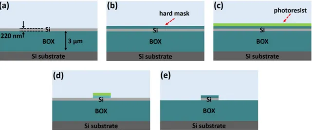
The fabrication process flow is reported in Fig. 2.15 and 2.17.
Fig. 2.15 Sequence of process steps for silicon waveguide fabrication.
The starting point is a 6" SOI wafer with 3µm thick BOX and 220nm thick silicon layer on top of that (Fig. 2.15 (a)). The whole wafer is covered by a layer of PECVD SiOx (Fig. 2.15 (b)) few tens of nanometers thick that is used as hard mask during the Si etch. Silicon waveguides and inverse tapers are fabricated at the same time, the layout is transferred on the photoresist layer (Fig. 2.15 (c)) by e-beam lithography. The area of photoresist that has been exposed is removed by the developer and the oxide layer is etched with reactive ion etching (Fig. 2.15 (d)). All the photoresist is then removed and, with a further dry-etch step, the layout is finally transferred on the silicon layer(Fig. 2.15 (e)).
The next Fig. 2.16 shows a top view of the fabricated silicon taper taken with a scanning electron microscope (SEM). It is long LSi= 25µm and it is highlighted in the centre of the
picture, its back-side is connected to the silicon waveguide, while the tip is on the right side.The silicon outside the trench is far enough to not interact with the propagating light.
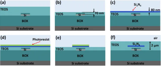
The EC consists of two overlapping parts: the bottom one is the silicon inverse taper, the top part is the Si3N4 core. The Si3N4core needs to be deposited on a flat surface, for this
reason it cannot be deposited directly after the last Si dry-etch step. In order to obtain a flat surface a conformal material, TEOS in this case, is deposited until it is thick enough that the surface bumps due to silicon waveguides are not visible any more (Fig. 2.17 (a)). The oxide hard-mask is not removed before the TEOS deposition since it does not interfere with the optical properties of the EC. At this point the TEOS layer is etched back (Fig. 2.17 (b)) till reaching a gap between the Si surface and the TEOS one of only 70 nm. Having a flat
28 III-V/SOI edge coupling
Fig. 2.16 SEM picture of the fabricated Si inverse taper part of the EC structure. surface, it is now possible to deposit the 80 nm thick Si3N4layer by LPCVD (Fig. 2.17 (c)).
On top of that it is spinned a layer of photoresist (Fig. 2.17 (d)) that is again exposed with the e-beam in order to transfer the Si3N4core shape from the design file to the wafer. The
material not covered by the photoresist is etched away (Fig. 2.17 (e)) and after removing the remaining photoresist the whole wafer is covered by a thick layer of TEOS that acts as waveguide cladding (Fig. 2.17 (f)).
Fig. 2.17 Sequence of process steps for EC fabrication.
Once the cladding has been deposited, the area in front of the EC is etched away in order to fabricate the trench in which the SOA is placed. Etched facets have small defect density meaning that low scattering losses can be expected.
2.2 The "kite" edge coupler 29
2.2.4
Testing
We used several approaches to test the fabricated EC. Each one had its particular purpose. The first test does not require actual butt-coupling and has been already presented in Sec. 2.1: a sequence of SSCs are fabricated one in front of the other. The light is injected in the sequence using a GC and goes through the SSCs so that the mode gets continuously expanded and compressed. At the end of the sequence there is an output GC where the output power is measured. Fabricating more than one sequence, with different number of SSCs, we could isolate the impact of the GC from the EC one, measuring how lossy is the conversion from the silicon waveguide mode to the SOA compatible mode and vice versa. This approach is really useful since even without having an actual butt-coupling measurement we can still characterize the quality of the fabricated device.
The results reported in the following Tab. 2.1 are the average insertion loss measured over nine different chips coming from the same wafer using the approach just described. These measured values are compared with the simulated ones. From this fabrication we measured facing SSCs with no separation, so that the Si3N4of the SSCs formed a unique shape; SSCs
with 1µm in-line separation so that the light was freely propagating for 1µm in the TEOS cladding (see Fig. 2.18 (b)); and SSCs with both 1µm in-line separation and 1µm lateral misalignment. Each value has been measured at 1550nm wavelength where the GC has the minimum insertion loss of 4.5dB. Comparing the simulated results with the measured ones we have good agreement.
Table 2.1 SSC insertion loss measurement
mean (dB) St Dev (dB) simulated (dB)
no separation 0.3 0.12 0.2
1µm in-line separation 0.46 0.10 0.4 1µm in-line&lateral 0.67 0.66 0.9
Fig. 2.18 (a) shows the test structures used for the on-chip coupling measurement, Fig. 2.18 (b) instead shows the details of two facing ECs. It is clearly visible the silicon waveguide tapering under the Si3N4core which is almost fully transparent.
The second test had the main goal of measuring the coupling loss between a tapered fiber and the EC, the tapered fiber was a commercial product with a MFD of MFDf iber = 3.5µm.
In this way we could also measure the horizontal and vertical misalignment tolerances. The fiber MFD was not identical to the SOA actual mode on which the EC design was optimized. For this reason we run 3D FDTD simulations in order to compute the expected coupling efficiency. The simulation result shown that the coupling loss should be 0.8dB.
30 III-V/SOI edge coupling
Fig. 2.18 (a) EC loss test structures and (b) and detail of two facing EC separated by 1µm. To complete this test we used the setup shown in Fig. 2.19(a), a continuous wave laser at 1550 nm was injected into the EC by positioning the tapered fiber in front of it, the light propagated for less than 1mm in a silicon waveguide and exited the PIC from a GC. Coupled with the GC there was a SMF attached to a power meter. To isolate EC loss from the rest of losses we first measured the power actually coming out of the tapered fiber with a photodiode power sensor. On the same SOI chip we had waveguides with different lengths in order to obtain the GC coupling loss and the waveguide propagation loss. The measured EC coupling loss was CL = 1.5dB when the tapered fiber was in the optimal position. Using the same setup we changed the fiber position in order to measure the misalignment tolerances of the EC. Fig. 2.19(b) shows the effect of the fiber x and y position variation on the EC coupling loss. The difference between the simulated and measured coupling loss could be due to the SOI facet roughness.
After fully characterizing the EC we wanted to also demonstrate the coupling between an active device and a SOI PIC. For this reason we completed the test by coupling a reflective-SOA (Rreflective-SOA) i.e. a reflective-SOA with a high reflective facet, with a simple SOI PIC using our developed EC. The RSOA was not integrated on the SOI chip, but it was actively aligned with it and glued together using epoxy. Further detail about the SOI-RSOA active alignment will be discussed in Chapter 5.
The RSOA device was fabricated by the Heinrich Hertz Institute (HHI), Fig. 2.20(a) shows a top view of the chip mounted over a silicon substrate. The RSOA chip was mounted there in order to be easily handled during automatic active alignment. The RSOA is long LSOA= 400µm, it has the anode contact on the top side (in the figure it has been wire bonded
![Fig. 2.4 Measured value of coupling loss moving the LD source both in the vertical and horizontal direction [6].](https://thumb-eu.123doks.com/thumbv2/123dokorg/2928353.18882/35.892.237.636.254.565/measured-value-coupling-moving-source-vertical-horizontal-direction.webp)