Contents
Abstract 5
Sommario 9
1 Introduction & Background 14
1.1 Toward High Speed and Energy - efficient Designs ... 14
1.2 Ultra-low Voltage (ULV) digital design: Characteristics and Issues18 1.3 Minimum Energy per Operation ... 22
1.4 Body Biasing as an efficient knob in ULV operation ... 27
1.5 Logic family exploiting Dynamic Body Biasing in ULV ... 30
1.6 Purpose of this work ... 33
2 Analytical Modeling for Dynamic Gate – Level Body Biased Logic Circuits 35 2.1 GLBB Operating Principle ... 36
2.2 Analytical Model ... 39
2.3 Design Criteria and Analysis Validations ... 50
2.4 Logic Gates with Stacked Transistors ... 57
2.5 Final Remarks on Design Criteria ... 69
3 Dynamic Gate – Level Body Biasing Technique in Bulk technologies 70 3.1 Physical constraints for gate-level body biasing technique ... 71
Abstract
4
4 Dynamic Gate – Level Body Biasing Technique in UTBB FD – SOI
technologies 85
4.1 UTBB FD – SOI Technology Overview ... 86
4.2 Design Optimization for Gate-level Body Biasing ... 89
4.3 Basic Gates: Design and Operating Characteristics ... 93
4.4 Final Remarks of Gate-level Body Biasing in UTBB FD-SOI... 96
5 Case studies: Application of the GLBB Technique to Arithmetic circuits 98 5.1 Mirror Full Adder ... 98
5.2 Ripple Carry Adder ... 102
5.3 Baugh Wooley Multiplier ... 107
5.4 Final Remarks of Gate-level Body Biasing Technique to Arithmetic Circuits ... 111
6 Conclusions 113
Bibliography 115
Acknowledgments 127
Abstract
Abstract
Power supply voltage (VDD) scaling below the transistor threshold volt-age (VTH) is one of the most effective approaches to achieve low energy consumption at the expense of large performance degradation and a much higher sensitivity to process variations and temperature fluctuations. While acceptable for niche markets, the delay and the robustness issues of con-ventional subthreshold CMOS circuits can be very limitative for a broader set of applications. In order to increase speed and robustness against pro-cess and temperature variations while maintaining high levels of energy efficiency, the forward body biasing (FBB) technique can be adopted. The FBB technique can be applied (also dynamically) at different levels of granularity ranging from the macro-block level to the transistor level. The key rationale for applying forward body biasing at the macro-block level is to amortize the area and the body control signal routing of a finer grained implementation. However, there is a cost to pay: when threshold voltage is reduced at the block level to compensate for variations and/or to provide a temporary speed boost, leakage power is increased for all the gates in the block, while speed-up would be needed only on timing critical gates. Bet-ter energy-delay tradeoffs can be obtained by reducing the body-bias con-trol granularity.
A feasible way to control body biasing at the transistor level is provided by the dynamic threshold voltage (DTMOS) logic. DTMOS logic uses tran-sistors whose gates are tied to their substrates. As the substrate voltage varies with the gate voltage, the threshold voltage of the device is dynami-cally changed. In the ON-state, the device threshold voltage drops, thus
Abstract
6 providing a much higher ON current with respect to a standard MOSFET configuration. On the other hand, the behavior of a DTMOS transistor in the OFF-state is similar to that of a regular MOSFET. However, the DTMOS configuration implies input capacitances significantly larger than that of a standard CMOS static gate. Additionally, DTMOS logic incurs in higher energy consumption due to unnecessary charge/discharge of the substrate for input signals that doesn’t produce a change in the output volt-age of the gate.
In this thesis a gate-level dynamic body biasing technique to overcome the energy limits of DTMOS logic gates, while also improving the gate switching speed has been developed. Logic gates, designed exploiting dy-namic body biasing technique exhibit input capacitances equal to those of the standard CMOS configuration. Moreover, when input signals switch without changing the logic gate status the body capacitances are not charged/discharged as occurs in DTMOS logic gates, thus enabling con-siderable energy saving.
Initially the gate level body biasing technique was modeled and analytical-ly justified. Initialanalytical-ly the inverter was adopted as reference circuit to devel-op the main design guidelines for the body biasing generator and the logic section of the gate. As an extension, logic gates with stacked transistors, (i.e. NAND2, NOR2) was also considered obtaining a good agreement be-tween the predicted and the simulated results.
Following, a preliminary analysis performed on basic gates demonstrated that the speed boosting provided by the gate-level body biased (GLBB) al-lows to reach performances which are unaffordable for both conventional CMOS and DTMOS configurations. Subsequently parasitic effects of body biasing were taken into account by post layout simulations of a GLBB mir-ror full adder and compared against its conventional CMOS and DTMOS
Abstract counterparts. The physical design of the compared circuits was carried out considering the design rules imposed by the ST 45 nm bulk CMOS triple-well technology. Despite of the large area occupancy compared to conven-tional CMOS, comparative post layout results have shown that the GLBB design style is, at the parity of leakage power consumption, able to obtain significantly higher performance with reduced total energy per operation consumption.
The ultra-thin box and body (UTBB) fully-depleted silicon-on-insulator (FD-SOI) technology is emerging as a valid platform to cope with ULV design bottlenecks in the more scaled technology nodes. The fully depleted channel of devices in this technology avoids the issue of the random do-pant fluctuation, thus reducing the impact of process variability. Moreover, the ultra-thin (<30 nm) buried oxide (BOX) guarantees a good electrostatic control of the channel and allows more effective body biasing with respect to bulk CMOS to be applied. The latter is a key feature of the UTBB FD-SOI technology which improves the benefits of the FBB technique for ULV designs in advanced technologies.
In order to reduce the area occupancy of the GLBB technique, several benchmarks has been implemented according to the GLBB technique in 28 nm STM UTBB FD-SOI technology for ULV logic design. The unique feature offered by the technology to integrate PMOS and NMOS devices into a common well configuration has been exploited to achieve improve-ments in terms of both performance and area.
The efficiency of the GLBB technique for ULV design in UTBB FD-SOI is evaluated by considering three arithmetic benchmarks in ascending or-der of complexity. As a first benchmark, the GLBB mirror full ador-der (FA) was considered. As a second benchmark a n-bit RCAs were designed ac-cording the evaluated techniques under a wide range of process and
tem-Abstract
8 perature (PT) conditions. For the TT/27°C condition, the DTMOS tech-nique shows higher energy consumption mainly due to the larger input ca-pacitances of DTMOS gates. On the contrary, GLBB and CMOS designs exhibit very similar Energy for the worst case operation (E W.C.O.) val-ues, even for long chains of FAs. The GLBB designs always demonstrate better performances than their competitors. For example, at VDD=0.4 V, an advantage of 33% and 46% is achieved in terms of speed and energy when compared to CMOS and DTMOS designs, respectively.
As third benchmark, a 4 x 4-bit Baugh Wooley multiplier was evaluated. At VDD = 0.3 V, the proposed approach leads to a delay reduction of about 30% with respect to a conventional static CMOS design. Such re-sults were obtained while maintaining similar energy consumption and at the only expense of about 13% larger area. Significantly better energy (39%) and area (34%). The above delay and energy benefits are main-tained over a wide range of PVT variations.
Sommario
Sommario
Lo scaling della tensione di alimentazione (VDD) al di sotto della tensione di soglia dei transistor (VTH) è uno degli approcci più efficaci per ottenere un basso consumo energetico a discapito di un’elevata riduzione delle pre-stazioni e una sensibilità molto più elevata alle variazioni di processo e di temperatura. Sebbene accettabile per un mercato di nicchia, l’elevato ritar-do e la riritar-dotta robustezza dei circuiti sottosoglia CMOS convenzionali possono essere molto limitativi per una gamma più ampia di applicazioni. Al fine di incrementare le prestazioni e la robustezza contro variazioni di processo e di temperatura, pur mantenendo elevati livelli di efficienza e-nergetica, la tecnica di polarizzazione diretta del bulk/body dei transistori (forward body biasing - FBB) può essere adottata.La tecnica FBB può essere applicata (anche dinamicamente) a diversi li-velli di granularità che vanno dal livello di macroblocco al livello di singo-lo transistor. Applicando la tecnica FBB a livelsingo-lo di macro bsingo-locco si riduce il numero di segnali destinati al controllo della tensione di body, riducendo così la complessità del routing. Di contro, si riduce la flessibilità di con-trollo della tensione di soglia dei singoli transistori con un impatto negati-vo sul consumo energetico. Diversamente, l’implementazione della tecnica FBB a livello di singolo transistore permette di gestire con minore granula-rità la tensione di body dei mosfet. Così facendo è possibile agire, incre-mentandone le prestazioni, solo sui transistori che sono coinvolti nella de-terminazione del path critico del circuito.
Un esempio di applicazione della tecnica FBB a livello di singolo transi-stor è rappresentato dalla logica a “tensione di soglia dinamica” (DTMOS). Tale logica utilizza transistor i cui terminali di gate sono
colle-Sommario
10 gati al substrato. Di conseguenza, la tensione di soglia del dispositivo cambia dinamicamente in funzione della tensione di gate e quindi della tensione di substrato. Pertanto, nello stato di ON, la tensione di soglia di-minuisce, garantendo così una corrente di ON più elevata rispetto alla con-figurazione standard CMOS. D’altra parte, il comportamento dei transistor in logica DTMOS nello stato di OFF è simile a quello della configurazione CMOS standard. Tuttavia, l'utilizzo della configurazione DTMOS provoca un significativo incremento delle capacità di input rispetto a una porta sta-tica CMOS. Inoltre, la logica DTMOS comporta un maggiore consumo di energia dovuto al verificarsi di eventi di carica/scarica del substrato non necessari per segnali di ingresso che non producono una variazione della tensione di uscita della porta.
In questa tesi è stata proposta una tecnica di polarizzazione dinamica del substrato (gate level body biasing - GLBB) da impiegare a livello di porta logica per ridurre il consumo di energia nelle porte logiche DTMOS e ga-rantire allo stesso tempo una maggiore frequenza di switching. L'imple-mentazione di questa tecnica consente di ottenere capacità di input identi-che a quelle delle porte logiidenti-che CMOS standard. Inoltre, quando la com-mutazione dei segnali di ingresso non produce un cambiamento di stato della porta logica, le capacità di substrato non si caricano/scaricano come avviene nella logica DTMOS, consentendo perciò un notevole risparmio di energia.
Inizialmente, è stato sviluppato un modello analitico per validare la tecnica proposta. In questa prima fase, l'inverter è stato adottato come circuito di riferimento per ricavare le principali linee guida per la progettazione del generatore di polarizzazione del substrato e della sezione logica della por-ta. Inoltre, sono state analizzate anche alcune porte logiche con transistor connessi in serie (ad esempio, NAND2 e NOR2), ottenendo un buon
ac-Sommario cordo tra i risultati predetti con il modello analitico e quelli ottenuti con le simulazioni.
Successivamente, è stata effettuata un'analisi preliminare su porte logiche basilari per dimostrare che l'impiego della tecnica di polarizzazione del substrato a livello di porta logica consente di ottenere prestazioni superiori alle configurazioni CMOS standard e DTMOS. In seguito, sono state effet-tuate anche simulazioni post-layout di un circuito "mirror full adder" rea-lizzato con la tecnica GLBB per includere gli effetti parassiti della polariz-zazione del substrato. I risultati di queste simulazioni sono stati confrontati con quelli ottenuti per lo stesso circuito realizzato con le tecniche CMOS standard e DTMOS. La progettazione dei circuiti da confrontare è stata re-alizzata utilizzando la tecnologia ST 45-nm bulk CMOS triple-well. I ri-sultati comparativi hanno dimostrato che la tecnica di progettazione GLBB, a parità di consumo di potenza di leakage, consente di ottenere un significativo incremento delle prestazioni con un ridotto consumo di ener-gia, a discapito di una maggiore occupazione di area rispetto alla logica CMOS convenzionale.
La tecnologia "ultra-thin box and body (UTBB) fully-depleted silicon-on-insulator (FD-SOI)" sta emergendo come una valida soluzione per la pro-gettazione di circuiti a bassissima tensione di funzionamento (ultra low voltage -ULV) in nodi tecnologici sempre più scalati. La presenza di un canale completamente svuotato nei dispositivi realizzati con questa tecno-logia consente di eliminare il problema della fluttuazione causale del dro-gaggio e quindi di ridurre l'impatto della variabilità di processo. Inoltre, il ridotto spessore dell'ossido sepolto (<30 nm) assicura un buon controllo elettrostatico del canale e quindi un più efficace impatto della tecnica di polarizzazione del substrato rispetto alla tecnologia CMOS convenzionale. Quest'ultima rappresenta la caratteristica chiave della tecnologia UTBB
Sommario
12 FD-SOI, che consente di incrementare i benefici della tecnica FBB nella progettazione di circuiti ULV implementati in nodi tecnologici avanzati. Diversi circuiti di test sono stati implementati nella tecnologia 28-nm STM UTBB FD-SOI allo scopo di ridurre l'occupazione di area dovuto all'uso della tecnica GLBB. Difatti, grazie alla peculiarità offerta da tale tecnolo-gica di integrare transistor PMOS a NMOS in una configurazione a sub-strato comune, notevoli miglioramenti sono stati ottenuti sia in termini di prestazioni che di occupazione di area.
L’efficienza della tecnica GLBB per progetti ULV in tecnologia UTBB FD-SOI è stata valutata considerando tre differenti circuiti aritmetici di test in ordine crescente di complessità. Il primo circuito di test considerato è stato un "mirror full adder". Il secondo circuito di test è stato un "ripple carry adder - RCA" a n bit, analizzato per studiare l'impatto delle differenti tecniche di progettazione in un'ampia gamma di condizioni di processo e temperatura. Nelle condizioni TT/27°, la tecnica DTMOS ha mostrato un elevato consumo di energia, principalmente dovuto alle elevate capacità di input nelle porte logiche DTMOS. Al contrario, i circuiti progettati con le tecniche GLBB e CMOS standard hanno esibito un analogo consumo di energia nelle condizioni operative peggiori (worst-case operation), anche in presenza di lunghe catene di full adder. Inoltre, il circuito GLBB ha mo-strato sempre le migliori prestazioni. Ad esempio, con una VDD di 0.4 V, il circuito GLBB consente di ottenere un vantaggio del 33% e del 46% in termini di velocità ed energia rispetto ai circuiti CMOS standard e DTMOS.
Infine, è stato analizzato come terzo circuito di test un moltiplicatore 4 x 4-bit Baugh Wooley. Con una VDD di 0.3 V, l’approccio proposto ha porta-to ad una riduzione del ritardo di circa il 30% rispetporta-to al circuiporta-to CMOS standard. Questi risultati sono stati ottenuti mantenendo inalterato il
con-Sommario sumo di energia, a discapito solo di un incremento di area del 13%. Da un confronto con la logica DTMOS si è ottenuto invece un risparmio di ener-gia di circa il 39% ed una riduzione dell’area del 34%. I precedenti benefi-ci in termini di ritardo ed energia sono mantenuti entro un'ampia gamma di variazioni PVT.
Introduction & Background
14
One
1 Introduction & Background
1.1 Toward High Speed and Energy - efficient Designs
The ever increasing demand for portable devices to achieve enhanced productivity, a better user experience and multimedia quality drive innova-tion in digital circuit systems. In the late 1990s, the first commercial phone weighed 16 ounces and had half-hour of talk time. This GSM phone equipped with a simple RISC processor run at 26MHz and supported a primitive user interface [1]. After a steady increase in clock frequency to roughly 300MHz in the early 2000s, there has been a sudden spurt towards 1GHz and beyond [2]. More than 10 years later a wide set of computing capabilities (such as video processing, augmented reality, etc.) are offered by portable devices. Figure 1.1 illustrates the major trends from 2004 to 2014 in smartphones and tablets relevant to digital circuits.
Introduction & Background
Figure 1.2: Real scaling trends over the years 1975-2010 obeying the Moore's law [3]. Figure 1.1: Application processor trends in smart phones from 2004 to 2014 [2]
Such impressive achievements have been obtained thanks to the miniaturi-zation of the integrated digital circuits. In 1965 Gordon Moore predicted that technology scaling will allow to increase the number of components to the double every 12-24 months at minimum economical cost [3]. This
Introduction & Background
16 trend has been followed by semiconductor industry as shown in Figure 1.2 increasing to millions the transistor count per chip.
In general, a CMOS technology when is scaled to the next generation node improves: (1) transistor and interconnection speed, (2) transistor density and (3) switching energy consumption [4]. Although portable devices have been taking advantage of technology scaling to offer higher performance, in the last years as technology nodes enters into the deep submicron era, leakage power consumption rises as a main issue.
To be more specific, traditional scaling of FETs consists in the reduction of supply-voltage ( ) and threshold - voltage ( ) to accommodate both performance and power requirements, but the increasing impact of leakage currents and number of transistors on a single chip has placed lim-its on this scaling strategy.
At circuit level, voltage scaling (with a fixed threshold voltage) has been demonstrated as the most efficient solution for power constrained applica-tions [5]–[9]. In 1991, some digital signal processors operated at the lower 3V range in the 0.8 µm node. The authors realized that 5V specifications could be relaxed for their performance requirements therefore they operate at lower voltage to dissipate less power [1].
Voltage scaling is certainly a very effective lever to reduce energy and power consumption at expense of performance. As it can be easily ob-served by Equation (1.1) leakage power has a linear dependency on :
(1.1)
Thus decreasing down to a voltage level lower than linearly re-duces leakage power by from 2.5 x to 9 x for various technologies as shown in Table 1.1
Introduction & Background Table 1.1: Leakage power saving from reduction [10]
Technology node (VDD - nominal) 65 nm (1V) 0.13 μm (1.2V) 0.18 μm (1.8V) VDD (subthreshold) 1 1.2 1.8 0.4 2.5 X 3 X 4.5 X 0.3 3.3 X 4 X 6 X 0.2 5 X 6 X 9 X
Additionally, as it is shown by the well-known equation of dynamic ener-gy consumed by a digital circuit in (1.2).
(1.2)
As is reduced, quadratic energy savings are obtained since effective switching capacitance are maintained. Again, scaling reduce considerable dynamic energy by from 60 x to 80 x as shown in Table 1.2
Table 1.2: Dynamic Energy saving form reduction [10]
Technology node (VDD - nominal) 65 nm (1V) 0.13 μm (1.2V) 0.18 μm (1.8V) VDD (subthreshold) 1 1.2 1.8 0.4 6.25 X 9 X 20.25 X 0.3 11.1 X 16 X 36 X 0.2 25 X 36 X 81 X
Although operation in sub threshold regime demonstrates significant pow-er and enpow-ergy saving compared to strong-invpow-ersion oppow-eration, significant performance loss and higher sensitivity to variations occur [11]–[24]. Such limitations have maintained subthreshold digital design for a strictly nar-row set of applications while a broader market demand high performance and energy-efficient designs.
Introduction & Background
18
Figure 1.3: NMOS transistor current contributions in subthreshold. (a) Sub-threshold current. (b) Gate current. (c) Junction current.[33]
1.2 Ultra-low Voltage (ULV) digital design: Characteristics and Is-sues
As is reduced to minimize energy per operation, FETs make the tran-sition from strong inversion with large gate overdrive to subthreshold op-eration in weak inversion. Current of a NMOS transistor operating in subthreshold regime has three main contributions as illustrated in Figure 1.3: (a) the subthreshold current , due to diffusion of minority carriers
between drain and source [25], (b) due to tunneling through the dielec-tric and (c) mainly due to band-to-band tunneling current across the thin depletion regions [26]. Because of the stronger dependence on the gate voltage, and tend to be much lower than at low voltages. Hence the NMOS current operating at subthreshold region represented in (1.3) is mainly dominated by .
Introduction & Background Subthreshold operation differs from strong inversion operation primarily because the depends exponentially on threshold voltage ( ) and gate
- source voltage ( ), while the typical strong inversion operation
on-current ( depends roughly linearly on and .
The exponential characteristic of drastically affect circuit behavior in
several aspects such as the exponential performance degradation, large pMOS / nMOS imbalance and higher sensitivity to variations.
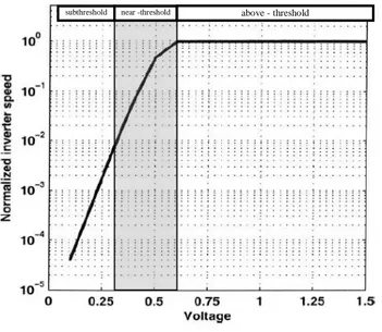
A first issue of circuits operating in subthreshold region is that the delay increase exponentially due to the dependency of the current on
and . As observed in Figure 1.4 the normalized speed of the basic in-verter has two clear stages as is reduced: (1) in strong operation region the speed slightly decrease with voltage, (2) in sub/near threshold, an ex-ponential decrease in speed is clear. Large performance decrease in subthreshold regime severely limits the range of applications to those re-quiring medium or slow speeds.
Figure 1.4: Relative inverter speed through all the power supply range
Introduction & Background
20 A second important issue in ULV digital designs is the high imbalance be-tween the nMOS and pMOS strength. Symmetrical pMOS and nMOS cur-rents ensure adequate noise margin, reasonably symmetric rise-fall transi-tions and reduce minimum voltage operation [27]. At subthreshold regime operation, the nMOS/pMOS imbalance is typically much higher than above threshold operation [28]–[30]. For example in the specific case of 65 nm technology the nMOS/pMOS imbalance is obtained by increasing pMOS strength by 7 at the expense of larger capacitances [31].
The large nMOS/pMOS imbalance at ULV operation has important conse-quences on the DC behavior. Figure 1.5 represents the model of an inverter for b) low and c) high voltage input. The on transistor Mn is equivalent to a current source, whereas Mp is equivalent to a resistance. From the result-ing equivalent model of the inverter the output voltage suffers a
volt-age drop across Mn [1], [27]:
(1.4) Similarly, for a high voltage input
(1.5)
Where are nMOS, pMOS strength respectively. From (1.4) and (1.5), the output levels are exponentially degraded as is reduced, and their values depend on the nMOS/pMOS strength ratio. In other words
Introduction & Background CMOS logic at ULV operation suffers a degradation in the output logic level, hence on the voltage swing [27].
A side effect of voltage swing degradation is the increase in the leakage power consumption of the subsequent logic gate. To be more specific a degradation of in the ouput voltage determines an equal increase in the gate-source voltage of the off nMOS transistor in the next logic gate. Thus a perfect nMOS/pMOS balance should be achieved by increasing the strength (i.e. increase the sizing and/or reducing ) of the weaker
tran-sistor.
Figure 1.5: a) Schematic of the inverter gate and equivalent representation for b) high input and c) low input voltages [33]
And third, as shown in (1.3) the exponential dependence of on means that variations due to random doping fluctuations has a larger im-pact than above threshold operation. Thus the previously discussed issues of subthreshold digital designs are more critical taking into account pro-cess (P) variation [32]. For example, the large impact in the nMOS/pMOS imbalance presented before increases ~2X taking into account process
var-Introduction & Background
22 iation. The data obtained from Monte Carlo simulations in the 65nm tech-nology is plotted in Figure 1.6 the shape of the PDF presents a mean value of and a standard deviation of . Hence the increasing factor of pMOS strength by 7 mentioned in the previous analysis is under-estimated taking into account process variations. Indeed this large underes-timation is due to the large variability of [33].
Figure 1.6: Probability density function of the nMOS/pMOS imbalance from 10,000 Monte Carlo simulations under itradie and interdie variations [33]
1.3 Minimum Energy per Operation
In ULV systems a repetitive short task is performed at a given wake up pe-riod . Thus, as shown in Figure 1.7, power consumption can be dras-tically reduced through duty cycling. Duty cycling systems contain two blocks: (1) a very simple always – on block that stores information and pe-riodically triggers a (2) more complex block which works in active mode
nMOS/pMOS imbalance
Introduction & Background for about 0.1% - 1% of the period and in sleep mode for most of the time according to the application [33].
Figure 1.7: Operation of duty - cycled blocks in Ultra Low Power systems.[33]
In duty-cycled ULV systems the average consumption is equal to
(1.6)
Where is the average power consumed by the always-on
blocks, and is the average power consumed by duty cycled block in sleep and active mode respectively. Since duty cycled block is far more complex than always on circuitry easily ceeds . Indeed in applications with a fraction of a second wake up period (or less) energy consumed by duty cycled blocks in active mode dominates . This justifies the extensive research in the last decade in digital circuit designs toward minimum energy per oper-ation. To be more specific ULV design should be optimized for low power consumption (always on block) and minimize energy per operation (con-sumed by more complex duty cycled block) during active mode.
For large classes of circuits, minimum energy consumption occurs when the voltage is scaled below the device threshold voltage ( ) [1],
Introduction & Background
24 [34]. In this region, energy consumption can be reduced by 20x compared to standard superthreshold ( > ) operation at the cost of circuit
per-formance [35].
Figure 1.8 illustrates that as is reduced a minimum energy point is achieved due to the trade - off between static and dynamic energy at a spe-cific power supply and voltage threshold .
Figure 1.8: Minimum Energy Operation Point for a fixed threshold voltage [35].
As shown in Figure 1.8 minimum energy consumption relies upon a com-promise between dynamic ( ) and leakage ( ) energies, expressed in (1.7), Errore. L'origine riferimento non è stata trovata. [36], [37], assuming rail-to-rail swing ( )
Introduction & Background
(1.7)
(1.8)
Thus taking into account the the total energy as presented in [1] is,
(1.9)
Where is the depth of critical path in characteristic inverter delay,
is the average effective switched capacitance of the entire circuit,
in-cluding the average activity factor, short circuit current, glitching effects, etc. and estimates the total width, related to the characteristic
inverter, that consumes leakage current.
Equation (1.9) indicates that the location of the minimum energy operation point is entirely determined by the operating scenario, environment and temperature of the circuit. To be more specific any decrease in or increase will push the optimum to lower values. On the contrary increase in or decrease will push the optimum to larger
values. These types of changes can occur for a given circuit without changing its intrinsic attributes.
Figure 1.9 shows the impact of varying the activity factor on the energy characteristics. The increases in proportion to the activity factor due to the amount of switched capacitance per operation thus optimum power supply shifts toward lower values. On the contrary Figure 1.10 shows the
Introduction & Background
26 impact of changing duty cycle on the energy characteristics. A longer idle time spent for each operations increments leakage energy consumption and the minimum energy point moves to higher voltages.
Figure 1.9: Energy versus varying workload in a 8-bit 8-tap FIR filter [1]
Introduction & Background
1.4 Body Biasing as an efficient knob in ULV operation
Even though energy has become increasingly important, the attention has focused on the high performance tail of the energy-delay Pareto curve. De-signers tried to minimize energy consumption while meeting high perfor-mance frequency constraints. As demonstrated by [33], [38], [39][40] body biasing is considered as an effective knob for tuning the transistor strength and the impact to alleviate issues raised by subthreshold operation such as large performance degradation and sensitivity to variations .
For this analysis an extended expression of (1.3) is presented taking into account the width, length of the transistor, usually written in the following form [25],[41]:
(1.10)
Where is the technology-dependent subthreshold current extrapolated for . In (1.10) the threshold voltage also depends on the drain-source voltage and bulk-source voltage through DIBL and body effect, respectively.
(1.11)
is the DIBL coefficient and is the body coefficient [4].
For a better insight, it is convenient to rewrite (1.10) and (1.11) according to [33]:
Introduction & Background 28 (1.12) (1.13)
Where the exponential dependence on and is highlighted and all other terms related to the transistor strength are grouped in the parame-ter .
From (1.13) the transistor strength can be tuned by three parameters: as-pect ratio , threshold voltage and statically or dynamically tuning the bulk voltage .
Is easy to observe that has a linear dependency in and an implicit dependence in which is significant for narrow or short channels. More specifically, an increase in leads to threshold increase due to narrow channel effect (RNCE) [25]. Additionally as shown in (1.9) the increase in transistor sizes will increment rising the energy consumption.
Theo-retically minimum energy circuits should use minimum sized. As a result, is not an effective knob to increase the strength of the transistor
A more effective knob to tune the strength of the transistor is and thanks to the exponential dependency on . As an example we compared two flavors offered in the 65nm technology: transistors are about 18 times stronger compared to transistors with the same
Introduction & Background Similarly body biasing has a significant impact in . Applying a Forward Body Bias (FBB) of transistor strength increased 2.3X compared to Zero Body Bias [33].
It should be mention that FBB can be applied dynamically to satisfy on-demand application requirements. Due to the high impact on the transistor strength and freedom to manage at different levels of abstraction (i.e.
gate-level, circuit-level, etc.) is an efficient knob to achieve minimum
energy consumption for a wide operating scenarios. This principle is better explained in the Figure 1.11. The location of the minimum energy opera-tion point is determined by the tradeoff between and thus and can tune the performance at run time in the most energy-efficient way. In point A ( ) (low activity), performance should be
in-creased by increasing since this leads to an exponential performance increase and energy decrease. On the other hand in point B ( ), performance should be increased by Body Bias, since this leads to an ex-ponential performance increase and a fairly small energy increase.
In conclusion the most powerful knobs to tune the performance at run time are the supply voltage and the body bias voltage . The above dis-cussed guidelines demonstrates that dynamic body bias should be used for circuits under timing constraints.
Introduction & Background 30 106 107 108 109 1010 0.1 1 105 106 107 108 109 1010 0.1 0.2 0.3 0.4 0.5 B E n e rg y p e r C y c le ( fJ ) Frequency (Hz) FBB=0 FBB=0.5 FBB=1 FBB=1.5 A B A P o w e e r S u p p ly ( V ) Frequency (Hz) FBB=0 FBB=0.5 FBB=1 FBB=1.5
Figure 1.11: Energy per cycle under timing constraints shows and as pow-erful knobs to tune the performance and energy at run time
1.5 Logic family exploiting Dynamic Body Biasing in ULV
The body biasing can be applied (also dynamically) at different lev-els of granularity ranging from macro-block level to the transistor level. The key rationale for applying, such a technique at the macro-block level is to amortize the silicon area and the body control signal routing complex-ity of a finer grained implementation. As a drawback, when is reduced at the block level to compensate for variations and/or to provide a
tempo-Introduction & Background
Figure 1.12: Schematic of Dynamic Threshold family of a) pMOS and b )nMOS transis-tors [19]
rary speed boost, leakage power is increased for all the gates in the block, while speed-up would be needed only on timing critical gates. Better ener-gy-delay tradeoffs can be obtained by reducing the body-bias control gran-ularity, at the expense of larger silicon area occupancy [42]–[44].
Dynamic Threshold MOSFET (DTMOS) is a logic family intro-duced in [19] which exploits dynamic body biasing at gate level without using additional circuitry control. In this logic family as the substrate volt-age varies with the gate voltvolt-age, the of the device is dynamically changed. When the device is turned ON, its threshold voltage is forced to drop, thus allowing a much higher ON current than a standard MOSFET. For example in the off-state for nMOS (pMOS) the characteristics are exactly the same as a regular MOS transistor. On the other side, in the on state is FBB and thus reduces the of the DTMOS transistor. The subthreshold slope of DTMOS improves and ap-proaches the ideal 60 mV/decade which makes it more efficient in subthreshold logic circuits to obtain higher gain [19]. It leads to higher on- current compared to conventional CMOS to drive more transistors or faster transitions and robustness.
DC characteristics of DTMOS and conventional CMOS are presented in Figure 1.13. Both show a very good noise margin however, due to higher drive current capability, DTMOS logic can have a higher number of
Introduction & Background
32 out, and therefore larger and more complex gates can be implemented without sacrificing the performance as presented in Figure 1.14.
Figure 1.13: Voltage Transfer Curve of conventional CMOS and DTMOS logic families
[19]
Figure 1.14: Delay versus Fan comparison for conventional CMOS and DTMOS logic families [19]
As a drawback of DTMOS the forward-biased has to be less than 0.6 V. This is to prevent forward-biasing the parasitic PN junction diode thus strong inversion operation is permitted applying limiter transistors which incur in energy consumption. As an additional drawback, the large body
Introduction & Background capacitance and resistance [45] of devices provide an additional RC delay in charging the substrate and the input nodes of the DTMOS logic gates [46]. Moreover, the substrate bias voltage of DTMOS logic gates would change also when input transitions do not imply output switching. This would charge and discharge the large body capacitances, thus wasting pre-cious dynamic energy [47]. All the above effects can erode the expected advantages of DTMOS circuits.
1.6 Purpose of this work
This thesis work focuses on the design of energy – efficient circuits ex-ploiting Gate-level Body Biasing (GLBB) technique, which has been pro-posed as an effective solution to increase speed at expense of very low en-ergy increasing. The first chapter presents an introduction to basic con-cepts and design issues related to circuits operating at ultralow voltage re-gime. The second chapter presents an accurate model of the technique with important design guidelines validated through Cadence Spectre simula-tions in 45nm Bulk CMOS triple-well technology[48]. The third chapter addressed more complex designs taking into account physical limitations of the technique implemented in Bulk CMOS triple-well technology [49], [50]. In the fourth chapter, after a briefly introduction to the UTBB FD-SOI technology and distinguish the superior body biasing efficiency com-pared to Bulk CMOS technologies, we propose single well configuration allowed by the technology to significantly reduce the area penalty of low-granularity body-biasing voltage control[51]. Finally, the fifth chapter pre-sents improved performance and energy characteristics of the GLBB tech-nique demonstrated by comparing several benchmarks (from basic gates to
Introduction & Background
34 a Baugh Wooley multiplier) to their conventional CMOS and DTMOS counterparts over a wide range of PVT variations[52],[53].
Analytical Modeling for Dynamic Gate – Level Body Biased Logic Circuits
Two
2 Analytical Modeling for Dynamic
Gate – Level Body Biased Logic
Cir-cuits
In this chapter the gate-level body biasing design (GLBB) technique that overcomes DTMOS logic family is explained and theoretically justified through an accurate closed-form analytical modeling. Initially, an inverter was adopted as reference circuit and the main static and dynamic behav-iors were modeled with the purpose of furnishing important guidelines to design efficient digital circuits under very low voltage operation. Modeling and design criteria derived for the inverter gate are then extended to more complex logic gates with transistors’ stacks. The theoretical analysis and the design considerations have been fully validated by comparing the re-sults predicted by models with Cadence Spectre simulations performed on different process corners and for different temperatures exploiting a com-mercial 45-nm CMOS technology. The good agreement between the pre-dicted and the simulated results makes the proposed modeling a valuable support during the circuit design phaseAnalytical Modeling for Dynamic Gate – Level Body Biased Logic Circuits
36 In the first chapter the FBB has been demonstrated as an energy-efficient knob to speed up a circuit and reduce the impact of variations. Furthermore, DTMOS has been analyzed as a logic family which exploits body biasing knob at gate-level. The main drawbacks of DTMOS configu-ration are: (1) reduced intrinsic speed advantages due to larger input ca-pacitances than a standard CMOS and (2) unnecessary charge and dis-charge large body capacitances according to the input wastes precious dy-namic energy [47].
In this chapter an energy efficient dynamic gate level body biasing (GLBB) technique [47] to overcome the speed and energy limits of DTMOS logic gates is presented. The proposed GLBB technique exhibit input capacitances equal to those of the standard CMOS configuration. Moreover, when input signals switch without changing the logic gate sta-tus, the body capacitances are not charged/discharged as occurs in DTMOS logic gates, thus saving considerable energy with respect to a DTMOS design.
2.1 GLBB Operating Principle
As shown in Figure 2.1 (a), the generic logic gate, designed according to the suggested approach, consists of two circuits: the logic sub-circuit which is responsible for the logical functionality of the gate and the body biasing generator (BBG) which manages the body voltage ( ) for both the pull-up and the pull-down networks. The BBG is a simple push-pull amplifier, which acts as a voltage follower for the output voltage VOUT, while decoupling the large body capacitances from the output node.
Analytical Modeling for Dynamic Gate – Level Body Biased Logic Circuits output voltage ( ) and the body voltage ( ) is reported for the falling
and rising output transitions, respectively.
When is equal to (0V), the BBG transfers a high (low) voltage
on the net, thus preparing the pull-down (pull-up) network for a faster logic gate switching. Since the MOSFETs of the switching network (either pull-up or pull-down) are already forward body biased before gate inputs’ arrival, the gate output transition is largely favored by a switching current significantly higher in comparison to the case of conventional body biasing scheme.
Speed and energy advantages exist with respect to a DTMOS configura-tion [47]. In fact, the transiconfigura-tion of the input signals is not slowed down from the body capacitive effects as occurs in DTMOS gates, whereas the high capacitive load seen by the BBG does not constitute a speed bottle-neck, since voltage is always established well before inputs’ transition. On the contrary, inspecting the behavior of the BBG circuit (see Figure 2.1 (b-c)), in the proposed scheme the logic sub-circuit benefits from the large body capacitances since they allow a slower transition for the body voltage and consequently a faster transition in the output. Additionally, when input signals switch without changing the gate output voltage, the BBG does not waste energy by charging/discharging the body capacitances.
Due to the FBB effects and the additional BBG circuitry, logic gates, de-signed as here proposed, show increased leakage current with respect to the conventional static CMOS counterparts.
Analytical Modeling for Dynamic Gate – Level Body Biased Logic Circuits
38
Logic Sub-Circuit
To the substrate of the Logic Sub-Circuit
V
IN VOUTV
BBBG Circuit
Pull-Up Network Pull-Down Network V OUT VB Voltag e Time VIN VB VOUT Voltag e Time VIN a) b) c)Figure 2.1: Logic gate with gate level dynamic body biasing (a) and transient behavior for falling (b) and rising (c) output voltage
Figure 2.2 depicts (a-b) leakage current ( ) versus delay curves in the
case of NAND2 and NOR2 logic gates for the conventional CMOS, DTMOS and GLBB implementations, respectively. At a parity of W, the GLBB technique shows leakage current higher than the other competitors. This means that, among the different evaluated choices, the GLBB style is the less suitable if the minimization of static power. On the contrary, if the speed requirement represents the main design aim, the GLBB style be-comes the most reasonable choice allowing higher performance to be
Analytical Modeling for Dynamic Gate – Level Body Biased Logic Circuits reached at the parity of leakage power consumption since the boosting ac-tion of the BBG allows the delay target to be reached using smaller transis-tors. Moreover, the GLBB technique allows performance ranges which are unaffordable for both CMOS and DTMOS configurations.
0 6 12 18 0.4 0.6 0.8 1.0 0 6 12 18 1.2 m CMOS DTMOS GLBB Ileak [A.U.] CMOS DTMOS GLBB (a) (b) 0.12 m w 1.2 m 0.12 m w Delay [A.U.]
Figure 2.2: Leakage current-delay plots for NAND2 (a) and NOR2 (b) logic gates
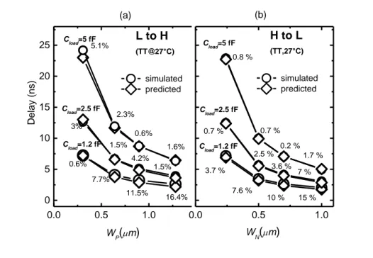
2.2 Analytical Model
In the following, analytical models for leakage current and delay of the inverter gate, designed according to the suggested technique, are derived. The developed models are then validated by comparing the predicted re-sults with Spectre simulations performed for the 45-nm ST CMOS Low Power technology. Moreover, the theoretical analysis is also exploited to define proper design guidelines (both for the BBG and the logic sub-circuits) with the main aim to obtain fast and power efficient subthreshold
Analytical Modeling for Dynamic Gate – Level Body Biased Logic Circuits
40 logic circuits. In particular, since reducing power consumption is a main concern in subthreshold design, the obtained design guidelines were ex-tracted by comparing the proposed approach with the conventional static CMOS style, which represents a good solution in terms of leakage power.
2.2.1 Leakage Current Analysis
Figure 2.3 illustrates the DC transfer function of the BBG sub-circuit. Note that, in the steady state, the BBG output voltage differs from and 0V. This is because a nMOS (pMOS) device is used for charging (dis-charging) the BBG output node (see Figure 2.1(a)). In the following and are used to indicate the voltage transferred by the BBG when
and , respectively. VOUT,BBG=VB VIN,BBG=VOUT VL VDD VDD VH
Figure 2.3: DC transfer function of the BBG
To estimate the leakage current, an analytical expression of the BBG out-put voltage is initially derived. The starting point is the following pair of subthreshold drain current equations for nMOS and pMOS transistors, re-spectively [25]:
Analytical Modeling for Dynamic Gate – Level Body Biased Logic Circuits , 1 , , , T N DS T N N TH N GS V V V n V V N DS e e I with 2 1, T N N OX N N V n L W C (2.1) , 1 , , , T P S D T P P TH P S G V V V n V V P SD e e I with 2 1, T P P OX P P V n L W C (2.2)
where N (P)is subthreshold current factor for the nMOS (pMOS)
tran-sistor, N (P) is the electron (hole) mobility, is the oxide capacitance per unit area, W is the channel width, L is the channel length, (with Boltzmann constant, absolute temperature and q elementary charge) is the thermal voltage, nN (nP) is the subthreshold slope factor for
the nMOS (pMOS) transistor, ( ) is the gate-to-source
(source-to-gate) voltage for the nMOS (pMOS) transistor, ( ) is the drain-to-source (source-to-drain) voltage of the nMOS (pMOS) transistor,
( ) is the threshold voltage of the nMOS (pMOS) transistor.
In (2.1), depends on through the drain induced barrier lower-ing (DIBL) effect and on body-to-source voltage ( ) through the body effect. Similarly, | | in (2.2) depends on source-to-drain voltage
Analytical Modeling for Dynamic Gate – Level Body Biased Logic Circuits 42 N BS N B N DS N D N TH N TH V V V V , 0, (2.3) , 0 , , P SB P B P SD P D P TH P TH V V V V (2.4) where, VTH0 ,N
0 ,P THV is the zero bias threshold voltage for the nMOS (pMOS) transistor, ND( P D ) and NB ( P B
) are the DIBL and body effect co-efficients of the nMOS (pMOS) device, respectively. The expression of the subthreshold drain current of the nMOS transistor in the BBG circuit is ob-tained by replacing in (2.1) and (2.3)
and . Similarly, the drain current in the pMOS transistor is
obtained by replacing in (2.2) and (2.4) and . By neglecting the contribution of the term in square
brackets in (2.1) and (2.2) and equating the currents of the nMOS and pMOS transistor, the following expression holds for the BBG output volt-age: . 1 ln 0 , 0 , 1 P B N B N D P D P n N n P n N n N P T V N n P TH V P B N D DD V N TH V P n N n OUT V B V (2.5)
From (2.5), both and can be easily evaluated, by substituting
and , respectively. Figure 2.4 shows the equivalent
sub-Analytical Modeling for Dynamic Gate – Level Body Biased Logic Circuits circuit + BBG) when VIN is low (Figure 2.4(a)) and high (Figure 2.4(b)),
respectively. Taking into account that for (
) is equal to , while when ( )
is equal to , the leakage current of the proposed inverter gate can be ex-pressed as (N(BBG) and P(BBG) indicate the nMOS and pMOS in the BBG, respectively):
0
, ) ( ) ( 0 ) ( , 0 , ) ( T P DD H BBG P B H BBG P D BBG P TH DD H T N H N B DD N D N TH V n V V V V V V BBG P V n V V V N IN BBG INV leak V e e I (2.6)
. ) ( ) ( 0 ) ( , ) ( ) ( 0 ) ( , ) ( T N L BBG N B L DD BBG N D BBG N TH L T P L DD BBG P B DD BBG P D BBG P TH V n V V V V V BBG N V n V V V V P DD IN BBG INV leak V V e e I (2.7)It is easy to verify that (2.6) and (2.7) are obtained exploiting subthreshold drain current expressions given in (2.1)-(2.4) where the term 1- VDSN nNVT
e , /
and 1- VSDP nPVT
e , /
are neglected since both and are greater than [33]. The first term in (2.6) and (2.7) is related to the leakage current in the logic section of the gate, whereas the second additive term captures the static current flowing through the BBG. From (2.6) and(2.7), it is clear that the proposed technique incurs in leakage penalties with respect to the conventional CMOS approach not only because of the FBB of the OFF transistors in the logic section but also because of the additional static cur-rent flowing through the BBG. In the following, we quantify this leakage current penalty.
Analytical Modeling for Dynamic Gate – Level Body Biased Logic Circuits 44 VB=VH VOUT=VDD MN(BBG) MP(BBG) MP MN
+
+
MP MN VB=VL VOUT=0 (b) EQUIVALENT CIRCUIT VOUT V B (a)Figure 2.4: Equivalent circuits for leakage analysis when is low (a) and high (b), re-spectively.
For a conventional static CMOS inverter, the leakage current in the steady state can be expressed as [3, 4]:
0
, 0 , T N DD N D N TH V n V V N IN INV leak V e I (2.8) . 0 , T P DD P D P TH V n V V P DD IN INV leak V V e I (2.9)It is worth noting that (2.8) and (2.9) can be also obtained from (2.6) and (2.7) by simply removing the impact of the BBG on leakage current (se-cond term in (2.6) and (2.7)) and imposing the (se-conditions of and
tran-Analytical Modeling for Dynamic Gate – Level Body Biased Logic Circuits sistor, the leakage penalty is obtained by calculating the ratio between (2.6) and (2.8) while, when the pMOS is the leaky transistor, the penalty in terms of leakage current is obtained by evaluating the ratio between (2.7) and (2.9): 0 , , ) ( , ) ( NT N TH T P BBG P TH DD H T N H N B V n V V n V V V N BBG P V n V IN INV leak BBG INV leak V e e I I (2.10) . , ) ( , ) ( PT P TH T N BBG N TH L T P L DD P B V n V V n V V P BBG N V n V V DD IN INV leak BBG INV leak e e V V I I (2.11)
From (2.10) and (2.11), the leakage penalty consists of the sum of two dif-ferent contributions. The first term isolates the effect of the FBB provided by BBG, which causes the threshold voltage reduction of leaky devices be-longing to the logical section of the gate. The second term provides the in-crement of the leakage current due to the additional push-pull amplifier, which is also dependent on the body voltage of devices belonging to the logical section of the gate. Moreover, such a term depends linearly on the ratio between the current factors of the leaky transistor in the logic section and the dual device in the BBG. According to (2.10) and (2.11) the impact of the proposed technique on leakage current can be reduced: 1) by lower-ing and increasing ; 2) by choosing an aspect ratio for the BBG tran-sistors much lower than the aspect ratio of the trantran-sistors used in the logic sub-circuit; 3) by using higher threshold voltage transistors for the MOSFETs in the BBG. All the conclusions here obtained can be easily ex-tended to a generic logic gate.
Analytical Modeling for Dynamic Gate – Level Body Biased Logic Circuits
46
2.2.2 Delay analysis
Without loss of generality, we initially consider that a 0 → 1 step input transition occurs. During the 1→ 0 output switching, the nMOS transistor is turned on and the inverter gate can be schematized through the equiva-lent circuit shown in Figure 2.5 (a). Here, represents the effective re-sistance of the nMOS, forward body biased by the BBG sub-circuit, and
is the overall capacitance on the output node which is given by the
sum of the load capacitance , the input capacitance of the
ad-ditional BBG circuit and the internal subthreshold capacitance [54] of
the logic sub-circuit. Modeling the output discharging as shown in Figure 2.5 (a), the H to L delay can be expressed as [55]:
, ) 2 ln( TOT N HL C R (2.12)
where is evaluated considering the transition from to [55]:
DD DD V V OUT N OUT DD N dV I V V R 2 / 2 (2.13)where and represent the drain-to-source voltage and the
drain current of transistor MN, respectively. The expression of the drain
current can be evaluated by using (2.1) and (2.3) and imposing
, and . For supply voltages higher than about
Analytical Modeling for Dynamic Gate – Level Body Biased Logic Circuits without loss of accuracy. This is because, for falling from to
, is always higher than 4 (~104 mV @ 27°C) [33].
VIN VOUT VB CLOAD VIN VIN CTOT CTOT VOUT VOUT (b) RN RP MN(BBG) MN MP (a)
Figure 2.5: Equivalent circuits to model inverter switching in the case of an L to H (a) and H to L (b) input transition
In order to obtain an easier expression for , the gain of the push-pull amplifier is here approximated by its DC value. Thus, according to the previous considerations, the body voltage during the H to L and L to H transition can be expressed as:
, H L AV V L H V V A V V OUT L OUT DD H B (2.14)
where A is the DC gain of the push-pull amplifier (i.e. the BBG). Using (2.14) to compute IN and solving the integral in (2.13), the H to L delay
Analytical Modeling for Dynamic Gate – Level Body Biased Logic Circuits 48
1 1 2 1 2 ) 2 ln( 2 2 DD N k V N DD k V N HL DD TOT HL k e V k V e k k V C N DDN DD (2.15) where T N DD H N B N TH DD V n V V V V N HL e k 0 , and
N T N B N D N A n V k / .The L to H delay can be evaluated in a similar way. The charging phase of the capacitance CTOT is modeled as shown in Figure 2.5 (b), where the
cur-rent flowing through the transistor MP is obtained from (2.2) and (2.4) with
the conditions: and . Also in this case the contribution due to the term eVSD,P/nPVT
can be neglect-ed. Finally, the L to H delay results to be:
1, 1 2 1 2 ) 2 ln( 2 2 DD P DD P k V P LH DD TOT LH k V k V e k k V C P DD (2.16) where T P L DD P B DD P D P TH DD V n V V V V V P LH e k 0 , and kP
DPAPB
/nPVT.As previously done for the leakage current, we evaluate the speed im-provement offered by the proposed scheme in comparison to the conven-tional static CMOS solution. In the case of a static CMOS inverter, expres-sions for H to L and L to H delays can be obtained from (2.15) and (2.16), respectively by canceling the effect of the FBB on the switching device (i.e. ). Thus, we find:
Analytical Modeling for Dynamic Gate – Level Body Biased Logic Circuits
1
, 1 2 1 2 ) 2 ln( 2 , , 2 , , , , V k DD NC C N DD k V C N C HL DD CONV HL k e V k V e k k V C NC DDNC DD (2.17)
1
, 1 2 1 2 ) 2 ln( 2 , , 2 , , , k DD PC DD PC V C P C LH DD CONV LH k V k V e k k V C PC DD (2.18) where N T N TH DD V n V V N HL e k 0 , , N T N D N n V k / , PT DD P D P TH DD V n V V V P LH e k 0 , and T P P D P n Vk / . It is worth noting that, in both (2.17) and (2.18), the output capacitance of the static CMOS inverter is indicated with
instead of in order to take into
ac-count the reduced output loading capacitance (i.e. the BBG loading capaci-tance is not included). From the ratio between (2.15) and (2.17), the delay reduction during the H to L transition is given by:
, 1 1 2 1 1 2 1 2 , , 2 2 , N DD k V N DD k V C N DD k V C N DD k V V n V N D N B TOT HL CONV HL k V e k V e k V e k V e e A C C N DD N DD N DD C N DD T N H N B (2.19)Similarly, the delay reduction during the L to H transition is obtained from the ratio between (2.16) and (2.18):
Analytical Modeling for Dynamic Gate – Level Body Biased Logic Circuits 50
. 1 1 2 1 1 2 1 2 , , 2 2 , P DD P DD k V C P DD C P DD k V P D P B V n V V TOT LH CONV LH k V k V e k V k V e A e C C P DD C P DD T P L DD P B (2.20)From (2.19) and (2.20), the delay reduction during H to L and L to H out-put transitions is enhanced by raising and lowering , respectively. In addition, since , the speed advantage of the proposed technique is increased if the input capacitance of the push-pull amplifier is minimized.
2.3 Design Criteria and Analysis Validations
The analytical modeling previously discussed is here exploited to define proper design criteria for both logic sub-circuit and BBG. From (2.10) and (2.11), a way to limit the static current flowing in the BBG consists of in-creasing the threshold voltage of devices employed in the push-pull ampli-fier. For this reason, both MN(BBG) and MP(BBG) are chosen as high threshold
voltage (HVT) transistors. Note that this choice emphasizes the inherent limitation of the static current in the BBG due to the reverse body biasing of its transistors and are always less than zero for MN(BBG) and
MP(BBG), respectively). Furthermore, since HVT transistors in the referred
CMOS technology have the same oxide thickness (i.e. the same COX) but
different doping profile in comparison to standard threshold voltage (SVT) devices, this choice does not have any additional impact on the gate load-ing capacitance. On the other hand, to guarantee higher gate speed,
![Figure 1.2: Real scaling trends over the years 1975-2010 obeying the Moore's law [3]. Figure 1.1: Application processor trends in smart phones from 2004 to 2014 [2]](https://thumb-eu.123doks.com/thumbv2/123dokorg/2875990.9851/15.748.110.639.108.398/figure-scaling-trends-obeying-moore-figure-application-processor.webp)
![Figure 1.5: a) Schematic of the inverter gate and equivalent representation for b) high input and c) low input voltages [33]](https://thumb-eu.123doks.com/thumbv2/123dokorg/2875990.9851/21.748.115.578.393.709/figure-schematic-inverter-equivalent-representation-input-input-voltages.webp)
![Figure 1.6: Probability density function of the nMOS/pMOS imbalance from 10,000 Monte Carlo simulations under itradie and interdie variations [33]](https://thumb-eu.123doks.com/thumbv2/123dokorg/2875990.9851/22.748.104.646.189.645/figure-probability-density-function-imbalance-simulations-interdie-variations.webp)
![Figure 1.9: Energy versus varying workload in a 8-bit 8-tap FIR filter [1]](https://thumb-eu.123doks.com/thumbv2/123dokorg/2875990.9851/26.748.219.527.210.465/figure-energy-versus-varying-workload-bit-fir-filter.webp)
![Figure 1.14: Delay versus Fan comparison for conventional CMOS and DTMOS logic families [19]](https://thumb-eu.123doks.com/thumbv2/123dokorg/2875990.9851/32.748.114.626.476.732/figure-delay-versus-comparison-conventional-cmos-dtmos-families.webp)