Superlattices and Microstructures 46 (2009) 223–226
Contents lists available atScienceDirect
Superlattices and Microstructures
journal homepage:www.elsevier.com/locate/superlatticesEpitaxial superlattices of ionic conductor oxides
A. Orsini
a,b,c,d,∗, P.G. Medaglia
a,b, S. Sanna
a,b,c,d, E. Traversa
c,d, S. Licoccia
c,d,
A. Tebano
a,b, G. Balestrino
a,baCNR-INFM Coherentia, Universita’ di Roma Tor Vergata, Via del Politecnico 1, 00133 Roma, Italy
bDipartimento di Ingegneria Meccanica, Universita’ di Roma Tor Vergata, Via del Politecnico 1, 00133 Roma, Italy cNAST Centre, Universita’ di Roma Tor Vergata, Via della Ricerca Scientifica 1, 00133 Roma, Italy
dDipartimento di Scienze e Tecnologie Chimiche, Universita’ di Roma Tor Vergata, Via della Ricerca Scientifica 1, 00133 Roma, Italy
a r t i c l e i n f o Article history:
Available online 20 December 2008 Keywords:
Fluorite superlattices Epitaxial thin film Pulsed laser deposition
a b s t r a c t
Pulsed Laser Deposition technique was used to engineer het-erostructures of Yttrium-stabilized Zirconia (YSZ) and Gadolinium-doped Ceria (GDC) on perovskite substrates like Neodymium Gallate (NGO) and Strontium Titanate (STO). Epitaxial superlattices of the same number of layers of both materials were deposited with each block thickness as thin as 2 unit cells up to 30 unit cells. X-ray diffraction (XRD) investigation of the (002) symmetrical reflection allowed to evaluate the amount of material deposited in each layer constituting the superlattices. (113) asymmetrical reflections were analyzed to investigate strain effects on YSZ and GDC lattice pa-rameters, evidencing the cube on cube growth of these films.
© 2008 Elsevier Ltd. All rights reserved.
1. Introduction
The possibility to grow thin films of oxide materials and to study their properties in the nanometer scale is of great importance in the development of micro solid oxide fuel cells [1]. Properties of thin films are usually different from those of bulk materials especially when the thickness of these films reach the nanometer range. A large enhancement in the ionic conductivity has been recently reported in the relevant literature for thin films with nanometric dimensions both in their thickness and in their grain size [2–4]. This effect has been observed for polycrystalline thin film of Yttrium -Stabilized Zirconia (YSZ) with a thickness of 17 nm (about 33 unit cells) [5] and Gadolinium-doped Ceria (GDC) with a thickness of 27 nm (about 50 unit cells) [6].
∗Corresponding author at: CNR-INFM Coherentia, Universita’ di Roma Tor Vergata, Via del Politecnico 1, 00133 Roma, Italy. Tel.: +39 06 72597245; fax: +39 06 72594328.
E-mail address:[email protected](A. Orsini).
0749-6036/$ – see front matter©2008 Elsevier Ltd. All rights reserved.
224 A. Orsini et al. / Superlattices and Microstructures 46 (2009) 223–226
The growth of heterostructures composed by nanometric layers of these materials (YSZ and GDC) might lead to achieving structures with an overall larger thick film having the same electrical properties of the ultra thin films previously cited. In fact, it has been reported that thin films made of alternated multilayers (at least about 30 u.c. each) of GDC and Zirconia showed a small enhancement in conductivity with respect to the parent materials [7]. This increase has been attributed to a combination of lattice strain and extended defects due to lattice mismatch between the heterogeneous structures. However these multilayer films were not epitaxial because sapphire was used as a substrate.
The aim of this work is the fabrication by pulsed laser deposition (PLD) of epitaxial superlattice films with blocks made of YSZ and GDC, two of the most studied electrolyte materials. These two materials have the same fluorite structure (Face Centered Cubic) with similar lattice constants, 5.14 Å for YSZ and 5.44 Å for GDC.
2. Experimental
The depositions were performed using an excimer laser charged with KrF, generating 248 nm wavelength pulses of 25 ns width. The laser beam, with an energy of 18 mJ per pulse, was focused in a high vacuum chamber onto a computer controlled multitarget rotating system. During the deposition, each target rotated around the perpendicular to the surface [8].
The two targets were prepared by sintering for 24 h at 1400◦C commercial 8% YSZ or 20% GDC
powders, previously pressed into discs of 3 cm in diameter. The substrates used for deposition were (100) SrTiO3(STO) and (100) NdGaO3(NGO) single crystals, placed at a distance of about 30 mm from
the target on a heated holder. As a background atmosphere molecular oxygen was injected through a narrow nozzle placed in close proximity to the plume. The average background p
(
O2)
in the chamberwas fixed in the 10−2–10−1mbar range.
The structural properties of the films were determined by means of x-ray diffraction (XRD) analysis using a
θ
–2θ
Bragg–Brentano diffractometer with Cu Kα
radiation. The symmetric (002) reflection of the superlattice, the asymmetric (103) reflection of the substrate and the (113) of the superlattice were investigated.3. Results and discussions
Superlattices composed by an equal number of unit cells of YSZ and GDC (N
×
N) (with N ranging from 2 to 30) were fabricated adjusting the number of laser shots during the ablation.Fig. 1shows the XRD plots of the superlattice thin films at angles near the (002) symmetric reflection of YSZ and GDC, which presented superlattice peaks aroundta central one, the average structure intensity peak(
SL0)
.For an equal number of unit cells in each layer, SL0should have a theoretical value of 33.86◦.
In the XRD plots (Fig. 1(a)) of the superlattices having thicker constituting blocks (from 8
×
8 to 30×
30), two satellite peaks were observed at lower angles(
SL−1–SL−2)
and at higher angles(
SL+1–SL+2)
. Otherwise the superlattices with thinner blocks (2×
2, 4×
4, 6×
6) presented only theSL−1–SL+1peaks (Fig. 2(b)).
The relative position between the satellite and the SL0peaks gives precise information on films
structure, allowing us to know the exact thickness of each layer and therefore to evaluate the exact number of laser shots necessary to complete a layer of YSZ or GDC [9]. The high quality of the superlattices diffraction peaks gives evidence of the heterostructure epitaxial growth due to the good lattice match between YSZ and GDC and the used NGO and STO substrates.
Even if the large mismatch in lattice parameter, namely 5.14 Å–5.44 Å for YSZ and GDC respectively and 3.8615 Å–3.905 Å for NGO and STO respectively, does not allow a cube on cube growth, however it is possible the epitaxial growth of fluorite oxides on perovskite substrates with an in plane rotation of 45◦between their unit cell axes, as shown inFig. 2.
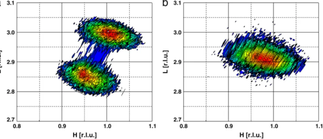
Fig. 3shows the reciprocal lattice maps around the (113) asymmetric reflections for the 30
×
30 (Fig. 3(a)) and 2×
2 (Fig. 3(b)) superlattice films. The investigation of superlattice asymmetric reflections was used in order to study the in plane orientation of the superlattice films with respect to the substrate and to separate the diffraction peaks of the two constituting materials.A. Orsini et al. / Superlattices and Microstructures 46 (2009) 223–226 225
Fig. 1. (a) Diffraction spectra of superlattices 14×14 (green line), 10×10 (red line) and 8×8 (blue line). (b) Diffraction spectra of superlattices 6×6 (green line), 4×4 (red line) and 2×2 (blue line). (For interpretation of the references to colour in this figure legend, the reader is referred to the web version of this article.)
Fig. 2. YSZ, GDC and STO unit cells sketch.
Fig. 3. (a) Reciprocal Lattice map of the (113) asymmetrical reflection of the 30×30 superlattice. (b) Reciprocal Lattice map of the (113) asymmetrical reflection of the 2×2 superlattice. Both maps are centered on the YSZ (113) reflection theoretical position.
226 A. Orsini et al. / Superlattices and Microstructures 46 (2009) 223–226
The simultaneous presence, at the same Phi-angle, of YSZ and GDC (113) reflection and of the substrate (103) reflection confirmed the cube on cube growth of YSZ on GDC and the 45◦ degree rotation between the crystalline axes of fluorite and perovskite materials. The GDC and YSZ lattice parameters calculated from the (113) reciprocal map relative to the 30
×
30 superlattice are in good agreement with the theoretical ones, indicating the absence of noticeable strain effects. The two separated peaks of the 30×
30 structure evolve in a single average structure peak corresponding to a lattice parameter of 5.29 Å both in plane and out of plane.4. Conclusions
A series of superlattices of YSZ and GDC ionic conductors with the fluorite structure were deposited by PLD on perovskite oxide substrates. It was possible to carefully control the deposition enabling to grow superlattices with constituting blocks as thin as 1 nm (2 unit cells).
Epitaxial structures were obtained as confirmed by XRD phi-scan plots. The high order of the realized structure should enhance the effect of high ionic conductivity in these YSZ-GDC superlattices. The possibility to study the conductivity as a function of the substrate (LAO, STO, NGO) and of the single block thickness could probably help to disentangle the phenomena contributing to the high oxygen ion conductivity in these heterostructures.
References
[1] D. Beckel, A. Bieberle-Hutter, A. Harvey, A. Infortuna, U.P. Muecke, M. Prestat, J.L.M. Rupp, L.J. Gauckler, J. Power Sources 173 (2007) 325–345.
[2] N. Sata, K. Eberman, K. Eberl, J. Maier, Nature London 408 (2000) 946.
[3] I. Kosacki, C.M. Rouleau, P.F. Becher, J. Bentley, D.H. Lowndes, Electrochem. Solid-State Lett. 7 (2004) A459. [4] A. Karthikeyan, C.L. Chang, S. Ramanathan, Appl. Phys. Lett. 89 (2006) 183116.
[5] I. Kosacki, C.M. Rouleau, P.F. Becher, J. Bentley, D.H. Lowndes, Solid State Ionics, Diffus. Reactions 176 (13–14) (2005) 1319–1326.
[6] A. Karthikeyan, M. Tsuchiya, C.L. Chang, S. Ramanathan, Appl. Phys. Lett. 90 (26) (2007) p 263108/1-3.
[7] S. Azad, O.A. Marina, C.M. Wang, L. Saraf, V. Shutthanandan, D.E. McCready, A. El-Azab, J.E. Jaffe, M.H. Engelhard, C.H.F. Peden, S. Thevuthasan, Appl. Phys. Lett. 86 (2005) 131906.
[8] A. Tebano, C. Aruta, N.G. Boggio, B.A. Davidson, P.G. Medaglia, F. Tozzi, G. Balestrino, ECS Trans. 3 (9) (2006) 55–63. Nanostructured Metal Oxides: Processing and Applications.