Reliability of RF MEMS Capacitive and Ohmic
Switches for Space Redundancy Configurations
.Andrea Lucibello
1, Romolo Marcelli
1, Emanuela Proietti
1, Giancarlo Bartolucci
1,2Viviana Mulloni
3, Benno Margesin
31 CNR-IMM Roma, via del Fosso del Cavaliere 100, 00133 Roma, Italy
2 University of Roma “Tor Vergata”, Dept. of Electronic Eng., Via del Politecnico 1, 00133 Roma, Italy 3 Fondazione B. Kessler, Via Sommarive 18, 38123 Trento, Italy
.. Work partially funded by the ESA Project AO/1-5288/06/NL/GLC on "High Reliability MEMS Redundancy Switch"
Abstract- In this paper RF MEMS switches in coplanar
waveguide (CPW) configuration designed for redundancy space applications have been analyzed, to demonstrate their reliability in terms of microwave performances when subjected to DC actuations up to one million cycles. As a result, both the investigated structures fulfill the current electrical requirements expected for redundancy logic purposes.
I. INTRODUCTION
Micro-electromechanical Systems (MEMS) have been studied for more than two decades, with the aim to develop DC and low frequency devices mainly for sensors and actuators to be used in quite different areas.
During the last decade, MEMS for high frequency applications (RF MEMS) have been developed for devices and sub-systems to be used in defense and space environments as well as for commercial devices [1].
The interdisciplinary skill typical of MEMS manufacturing has been enriched by the necessity of additional considerations in terms of high frequency design, technology and reliability in harsh environment, even including mechanical analysis [1][2][3] and charging effects [4][5][6].
Moreover emerging and future autonomous wireless communication systems require highly reliable electronic components with very low power consumption, and micro-machined devices represent a promising technology to meet this demand. RF-MEMS are specific micromechanical switches designed to operate at RF-to-millimeter-wave frequencies (0.1 to 100 GHz). Such RF switches have been demonstrated with low loss, low power consumption, low distortion, and higher off state isolation as compared to p-i-n diodes or field effect transistors. However, before such switches can be used in commercial or space applications, they must demonstrate the ability to switch reliably over billions of cycles, or, as it is the case of a redundancy switch, to maintain their electrical and RF performances for
a very long time and guarantee the switch actuation even after ten years. The presence of a mechanical contact introduces a whole new class of reliability issues related to both mechanical and electrical phenomena [7][8]. For the above reasons, Radio Frequency (RF) micro-electromechanical system (MEMS) switches are a contender for future low-power high-frequency wired reconfigurable networks and wireless communication systems [9]. These devices have the potential to overcome the limits of today’s equivalent implementations that use only traditional solid-state technology. In fact, all RF-MEMS devices (not only RF switches) maintain good miniaturization and they can be integrated with solid state circuits (e.g. either placed on the semiconductor wafer back-end-of-line inter-level dielectrics, or wiring levels, or independently, in the semiconductor component package). RF-MEMS devices exhibit almost zero power consumption, extremely good RF linearity, and high quality factor (Q) for tuning. Linearity metrics of input intercept second and third order harmonics (IIP2 and IIP3) both can achieve power levels better than 70 dBm [10].
From the technology standpoint, they can be manufactured by a low-cost process compared to other RF and microwave solid-state integrated circuits (e.g. RF Silicon on Insulator (SOI), Gallium Arsenide (GaAs) [11]). In particular, RF-MEMS can be made using standard foundry silicon processes. Actually, silicon based RF-MEMS are very easy to be micro-machined, can be integrated with mature semiconductor technology processes, and have the potential for wide proliferation across the global semiconductor foundry business. Additionally, Si RF-MEMS technology is compatible with the integrated circuits for digital, analog and RF mixed signal environments, making it possible to realize high frequency RF modules featuring a high level of integration (e.g. network-on-chip (NOC), and system-on-chip (SOC)). Another very attractive advantage for integration with Si-based technologies relates to the switch mechanical properties, with the possibility to obtain movable parts
through electrostatic, magnetic or thermal excitation, thus resulting in devices featuring a tunable behavior [12]. Despite these positive aspects, all the above and further benefits go along with a series of present-day shortcomings, which are mostly related to the maturity of the design methodologies and semiconductor fabrication processes. In terms of future applicability of these RF-MEMS to high-volume low-cost wired and wireless telecommunication markets, there are a lot of new applications that can be realized. The integration dilemma and potential MEMS paradigm shift that these new technologies have introduced is also accompanied by a lack of fabrication process standardization, big design flow impact, a limited reliability database, and poor knowledge of aging mechanisms and reliable design practices.
In this paper the weaknesses and the strengths for the reliability of this technology have been analyzed by means of the microwave characterization based on DC cycling tests on different kind of RF-MEMS switches.
II. SWITCH TECHNOLOGY AND EXPECTED PERFORMANCES
The switches have been produced within an international project in collaboration with the European Space Agency (ESA) with the target to develop a reliable redundancy switch for space applications. Micro-electromechanical switches have been designed in coplanar waveguide configuration (CPW), with central conductor leading the RF signal and lateral ground planes, and they are minded for exhibiting an insertion loss of less than 1 dB for the final redundancy component (typically 0.2-0.4 dB per single switch).
Switch Test of the building block single pole single throw (SPST) is very important to release the feasibility of the basic structure useful to implement more complicated configurations like single pole double throw (SPDT) and Matrices. The basic questions needing an answer are: (i) technology yield (statistics of the SPST device on the same wafer), (ii) maximum allowed number of actuations (mechanical limitations), (iii) lifetime (dynamic response, total actuation time, charging processes).
Several configurations have been tested to investigate mechanically stable, low-loss, negligibly charged devices. Specifically, a shunt capacitive and an ohmic series device have been manufactured and tested.
RF-MEMS switches, as their traditional counterpart, can be realized as either normally open or normally close switches. Both topologies can be realized with resistive-based (ohmic) or capacitive-resistive-based devices, depending on whether the device exhibits a metal-to-metal contact, rather than a Metal-Insulator-Metal (MIM) structure. An ideal series switch acts as an open circuit when it is in its rest position (no actuation voltage applied), or it acts as a low impedance path for the RF signal when the right actuation voltage is applied.
A shunt device exhibits instead a low impedance path for the RF signal when it is not actuated, or a high impedance path for the RF signal from the input port versus the output one (a low-impedance path to ground) when actuated.
Capacitive switches have a thin dielectric layer deposited on the transmission line avoiding the metal-to-metal contact, and the short-to-ground effects is obtained with the increasing of the MEMS capacitance, acting as a low impedance path for high frequency signals. The mechanical system implemented to obtain the change of state is quite simple: a suspended gold membrane over the transmission line, when electrostatically collapsed, connects the input with the output ports in the series configuration, or the input port to ground in the shunt topology. The RF-MEMS switches tested and analyzed in this work at CNR-IMM have been manufactured by the Bruno Kessler Foundation (FBK) of Trento (Italy).
The SPST configurations, to be successively used in a SPDT redundancy device, are shown in Fig. 1 (a) and in Fig. 1 (b). In Fig. 2 a schematic diagram of the cross section is also shown, with the materials used in the thin film technological steps.
(a)
(b)
Fig. 1. Ohmic series switch (a) and shunt capacitive configuration (b) tested for this work. Both switches are double clamped devices. Such a solution usually improves the mechanical reliability and the electrical performances.
Cantilevers are preferred for exhibiting lower losses, but technological constraints for the membrane flatness are more difficult to be fulfilled.
Fig. 2. RF-MEMS schematic cross section, with half-bridge shown and evidence for the polysilicon feeding lines used for the electrostatic actuation, metal underpass (interrupted for series switches and continuous
for shunted configurations). The movable membrane is far from the substrate 2.8 μm and it is released after plasma etching. The substrate is a
high resistivity silicon wafer 525 μm thick. LTO stands for low temperature oxide (used for the MIM capacitance defined by thecollapsed
membrane and the central conductor of the coplanar structure). TiN has been used in the metal underpass for compatibility with processe to be
performed below the bridge.
The general requirements for the exploited devices are for isolation better than 20 dB, and insertion losses not exceeding 0.3-0.4 dB for wideband applications. Of course, a shunt configuration is intrinsically limited in band because of its resonant response, while the ohmic series device is designed to have a broadband response.
To decrease the dependence of the exploited devices on the charging processes, dielectric pillars have been manufactured under the metal beam, to prevent the full contact between the bridge and the dielectric lateral pads used for the electrostatic actuation. In this way, an air gap is always present, and charging of the full device is maintained under control [13][14].
II. TEST BENCH SET UP AND METHODOLOGY FOR THE MEASUREMENTS:TEST SET-UP
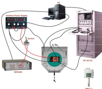
A remotely controlled Agilent HP8510C Vector Network Analyzer with a Karl Süss probe station equipped with ground–signal–ground RF |Z|-probes, and DC probes for actuation purposes, have been used to measure the scattering electrical parameters of the switches. The devices under test (DUT) have been measured under nitrogen flux controlled ambient environmental conditions. Measurements were taken performing a short–open–load– thru calibration in the frequency domain up to 40 GHz. The test bench is composed of the instruments shown in Fig. 3.
Fig. 3 : Test Bench Set-Up used for measuring the SPST devices, composed of:Dual Power Supply for the electrostatic actuation, VNA, Arbitrary Waveform Generator WFG600, Temperature and Humidity (T-RH) Sensor.The DUT is kept under nitrogen flow. The test conditions are:
Temperature = 23÷24 °C; RH ≈ 30%. SOLT Calibration from 45 MHz to 40 GHz has been performed, imposing an input power P=3 dBm. The
set-up is fully automated by means of a PC remote control based on the VEE Agilent software.
A. First step Bias:
A first slow ramp voltage, with ramp rate 1 V /sec, has been imposed to the DUT to measure the actuation voltage Vact, corresponding to a sudden change of the S-parameters measured by the VNA. The maximum voltage Vmax>Vact corresponds to an improved stability of the electrical response of the device when it is actuated. When charging effects are negligible, as a rule of thumb Vmax=Vact+5V can be chosen. Then, at Vmax the S-parameters are recorded. After that, a decreasing ramp is imposed to the DUT and the de-actuation voltage (Vdeact) is recorded. It is worth noting that the de-actuation voltage is lower than the actuation one due to the presence of surface and Wan der Waals forces, which are negligible before the actuation [1].
B. Second step Bias:
A unipolar positive pulse train is imposed to the DUT with a period T=2 msec and a Duty Cycle D=50%. The amplitude of the pulse train is equal to Vmax. At this step the switch is subjected to cycles (from 102 to 106 cycles). It
is common practice that a preliminary number of actuations, up to 102, can be considered as a procedure for exercising
the mechanical structure, eventually eliminating residuals of the bridge release under the beam, and contributing to a reliable mechanical response. The imposed pulse train is schematized in Fig. 4. A train made by positive pulses is generally preferred for simplicity in real applications, and by using only positive pulses residual unwanted charging can be immediately evidenced for monitoring it and for implementation purposes.
Fig. 4. Methodology used for the reliability measurements. The measure has been sub-divided in two main steps for recording both the actuation voltage
and the DUT response after cycling.
In the following Fig. 5 is shown the Isolation response of a Series Double Clamped Ohmic switch, i.e. when the device is not actuated and the bridge is in the up position.
0 10 20 30 40 -70 -60 -50 -40 -30 -20 -10 0 S11 first act S21 first act S11 after 10^2 S21 after 10^2 S11 after 10^3 S21 after 10^3 S11 after 10^4 S21 after 10^4 S11 after 10^5 S21 after 10^5 S11 after 10^6 S21 after 10^6 Is olat ion [ dB ] Frequency [GHz]
Fig. 5. Isolation response of the Series Double Clamped Ohmic switch shown in Fig. 1 (a).
The Isolation is always below -20 dB for an extended frequency range and no change has been measured after the reliability test, as all the curves overlap each other. In Fig. 6 are shown the Return Loss and the Insertion Loss, i.e. the switch electrical response when the device is actuated, giving a measure not only of the losses but also of the electrical matching at the input port. As a result, exception done for negligible oscillations, losses are contained within a fraction of dB (-0.4 dB up to the beginning of the millimeter wave range) and a quite good matching is also obtained, looking at Return Losses below -20 dB up to 40 GHz. Negligible worsening of the Return Loss has been measured after the reliability test. In the Table I are summarized the measured actuation and de-actuation voltages. The Actuation Voltage variation range is between 48V and 47.5V (quite stable) and small instabilities in the De-Actuation Voltage have been recorded. 0 10 20 30 40 -70 -65 -60 -55 -50 -45 -40 -35 -30 -25 -20 -15 -10 -5 0 RL first act RL after 10^2 RL after 10^3 RL after 10^4 RL after 10^5 RL after 10^6 Re tu rn Lo ss [d B] Frequency [GHz]
Fig. 6. Return Loss of the Series Double Clamped Ohmic Switch.
0 10 20 30 40 -2.2 -2.0 -1.8 -1.6 -1.4 -1.2 -1.0 -0.8 -0.6 -0.4 -0.2 0.0 IL first act IL after 10^2 IL after 10^3 IL after 10^4 IL after 10^5 IL after 10^6
In
ser
tion Loss [
dB
]
Frequency [GHz]
Fig. 7 Insertion Loss of the Series Double Clamped Ohmic Switch. TABLE I
Actuation Vact and De-Actuation Vdeact Voltages of the Series Double Clamped Ohmic Switch.
Cycles
V
act[V]
V
max[V]
V
deact[V]
10
048
53
41
10
248
53
41
10
348
53
36.5
10
448
53
41
10
547.5
52.5
36
10
647.5
52.5
41.5
Shunt switches exhibit also good performances, as it is shown in the following plots, where the same quantities already defined for the series ohmic device are presented. In this case, the actuation corresponds, as already outlined in the definition of the device functionality, to a resonating wideband response, centered, for the purposes of the present contract, between 10 and 20 GHz. 0 10 20 30 40 -1.2 -1.0 -0.8 -0.6 -0.4 -0.2 0.0 IL first act IL after 10^2 IL after 10^3 IL after 10^4 IL after 10^5 IL after 10^6
Inse
rtion Loss
[dB]
Frequency [GHz]
Fig. 8. Insertion Loss performances for the shunt capacitive configuration.
Fig. 9. Return Loss of the shunt capacitive device.
0 10 20 30 40 -35 -30 -25 -20 -15 -10 -5 0 S11 first act S21 first act S11 after 10^2 S21 after 10^2 S11 after 10^3 S21 after 10^3 S11 after 10^4 S21 after 10^4 S11 after 10^5 S21 after 10^5 S11 after 10^6 S21 after 10^6
Is
olat
io
n [
dB]
Frequency [GHz]
Fig. 10. Isolation of the shunt device when actuated.The actuation and de-actuation voltages are given in the following Table II.
Table II. Actuation and De-Actuation Voltages measured for the Shunt Double Clamped Capacitive Switch configuration.
Cycles
V
act[V]
V
max[V]
V
deact[V]
10
032
37
32
10
234
39
32
10
335
40
33
10
436
41
34
10
537
42
34
10
645
50
35
The above measurements on the ohmic series and on the shunt capacitive configurations clearly exhibit state-of-art performances because of the low insertion loss for series (down) and shunt (up) switches (-0.4÷-0.2 dB at 20 GHz). Making a comparison between the Table I and Table II the ohmic configuration is characterized by a more stable actuation and de-actuation voltage with respect to the shunt one. This can be due to residual charging effects which are more evident in the capacitive switches, as pointed out by the slight but progressive increase of the actuation voltage. Because of the complementary functionalities of the exploited configurations, the series ohmic device has been designed and it will be mainly used for imposing the transmission properties of SPDT devices, while the shunt one will be considered for enhancing the isolation performances of the redundancy switch. 0 10 20 30 40 -50 -45 -40 -35 -30 -25 -20 -15 -10 -5 0 RL first act RL after 10^2 RL after 10^3 RL after 10^4 RL after 10^5 RL after 10^6
R
e
tu
rn L
o
ss [
d
B]
Frequency [GHz]
IV. CONCLUSION
RF MEMS switches have been demonstrated to be promising for replacing the bulky electro-mechanical switches currently used in redundancy networks, assuring similar or even better electrical performances, and leading to a drastic reduction of the size and the weight of the overall system. As a strict requirement, redundancy switches in MEMS technology have to survive up to 10-15 years without any degradation in their electromechanical and electromagnetic properties. In this paper, the experimental results concerning the mechanical reliability of shunt and series RF-MEMS switches, designed and manufactured for redundancy space applications, have been presented. In order to understand the RF MEMS long-term mechanical reliability, RF measurements after cycling have been performed on several devices up to 1 milion actuations. The measured isolation and insertion loss after 106 cycles are better than -20 dB and -0.4 dB respectively,
up to a frequency of 20 GHz, making them suitable for space reliable applications. Further long-term measurements are in progress for obtaining better information in terms of residual charging.
REFERENCES
[1] S.D. Senturia, Microsystem Design, Springer Science, New York, USA, 2001.
[2] G.M. Rebeiz, RF MEMS Theory, Design, and Technology, 1st Ed.; John Wiley & Sons: Hoboken, New Jersey, USA, 2003. [3] Romolo Marcelli, Daniele Comastri,Andrea Lucibello, Giorgio De
Angelis, Emanuela Proietti, and Giancarlo Bartolucci: “Dynamics of RF Micro-Mechanical Capacitive Shunt Switches in Coplanar Waveguide Configuration”, InTech Publisher in the on-line Book "Microelectromechanical Systems and Devices", ISBN: 978-953-51-0306-6, Editor Dr Islam Nazmul, The University of Texas at Brownsville, USA DOI: 10.5772/28251
[4] Romolo Marcelli, George Papaioannu, Simone Catoni, Giorgio De Angelis, Andrea Lucibello, Emanuela Proietti, Benno Margesin, Flavio Giacomozzi, François Deborgies: "Dielectric Charging in Microwave Micro-electro-mechanical Ohmic Series and Capacitive Shunt Switches", IOP Journal of Applied Physics, Vol. 105, No. 11, pp.114514-1 - 114514-10
[5] R. Marcelli, A. Lucibello, G. De Angelis, E. Proietti, G. Papaioannou, G. Bartolucci, F. Giacomozzi, B. Margesin "Characterization and Modeling of Charging Effects in Dielectrics for the Actuation of RF MEMS Ohmic Series and Capacitive Shunt Switches, Microelectromechanical Systems and Devices", InTech Publisher in the on-line Book "Microelectromechanical Systems and Devices", Editor Dr Islam Nazmul, The University of Texas at Brownsville, USA, ISBN: 978-953-51-0306-6, InTech
DOI: 10.5772/29299
[6] R. Marcelli, G. Bartolucci, G. Papaioannu, G. De Angelis, A. Lucibello, E. Proietti, B. Margesin, F. Giacomozzi, F. Deborgies: “Reliability of RF MEMS Switches due to Charging Effects and their Circuital Modelling”, Microsystem Technologies, Vol. 16, No. 7, July 2010, pp. 1111-1118.
[7] J.Maciel. “Recent Reliability Results in RF MEMS”. Proceedings of the 2005 IEEE MTT-S Int. Microwave Symposium, June 2005. [8] J. L. Zunino III et al. “Micro-electromechanical Systems (MEMS)
Reliability Assessment Program for Department of Defense Activities”. Proceeding of the 2005 NSTI Nanotechnology Conference and Trade Show (Nanotech), 3:463–466, May 2005.
[9] G.M. Rebeiz. “RF MEMS in Full CMOS Radio SOC”. Proceedings of the 2005 MTT-S International Microwave Symposium, pages 36–56,192–201, June 2005
[10] Z. Zhang, X. Liao, L. Han and S. Su "A GaAs MMIC-Based Inline RF MEMS Power Sensor" Proceed. of IEEE SENSORS 2009 Conference
[11] Anna Persano, Augusto Tazzoli, Adriano Cola, Pietro Siciliano, Gaudenzio Meneghesso, and Fabio Quaranta: “Reliability Enhancement by Suitable Actuation Waveforms for Capacitive RF MEMS Switches in III–V Technology”, Journal of Microelectromechanical Systems, Vol. 21, No. 2, April 2012, pp. 414-419.
[12] R. Plana “What’s Hot in RF Components and Systems”. Microwave Journal, February 2006.
[13] Giorgio De Angelis, Andrea Lucibello, Emanuela Proietti, Romolo Marcelli, Giancarlo Bartolucci, Federico Casini, Paola Farinelli, Giovanni Mannocchi, Sergio Di Nardo, Daniele Pochesci, Benno Margesin, Flavio Giacomozzi, Olivier Vendier, Taeyoung Kim, Larissa Vietzorreck: “RF MEMS ohmic switches for matrix configurations”, International Journal of Microwave and Wireless Technologies, Vol. 4, Issue 4, pp. 421-433.
[14] P. Blondy, et al. “Dielectric less capacitive MEMS switches”, IEEE, MTT-S Int. Microwave Symp. Digest, 6–11 June 2004, vol. 2, 573–576.