Facolt`
a di Scienze Matematiche, Fisiche e Naturali
Corso di Laurea Specialistica in Tecnologie Informatiche
Tesi di Laurea
Libra.Net: Single Task Scheduling in a
CPU-GPU Heterogeneous Environment
Candidato Stefano Paganucci
Relatori Controrelatore
Dott. Antonio Cisternino Prof. Marco Vanneschi
Dott. Cristian Dittamo
Un grazie particolare ad Antonio e Cristian per l’aiuto ed il sostegno durante il lavoro, per i pranzi insieme e le chiaccherate. A Nicole, Gabriele, Alessandro, Matteo e Liliana per la bellissima esperienza che `e stata LOA Mobile e per le successive serate insieme per locali pisani. A Simone per i consigli ed il confronto informatico durante tutto il corso di studi. Ad Andrea per l’aiuto reciproco durante la preparazione degli esami e le serate fuori dal comune.
Per tutto quello che abbiamo passato insieme, grazie a tutti gli amici di sempre: Simo, Matte, Barbara, Diego, Monica, Fritz, Carmine, Marco, Oliver, Hanz, Roberto (il Pacio). Ai compagni della classe pi`u mitica della storia, la 5 Bst, per le gite, le infinite risate e l’amicizia che ancora oggi ci lega tutti. Insomma, un grazie enorme a tutti gli amici.
Agli zii e ai cugini: Giusy, Luca, Liviana, John, Alessio e Michele. A nonno Beppe, nonna Irma, nonno Livio e nonna I`e che con il loro sostegno hanno reso possibile tutto questo. A Irene e Babbo per sopportarmi ogni giorno e per l’enorme affetto di-mostratomi.
A Eli, perch´e senza di lei non avrei superato i momenti difficili, perch´e mi ha capito e perch´e `e sempre riuscita ad allietare ogni momento.
Alla mia mamma, per aver sempre creduto in me e perch´e so quanto avrebbe voluto condividere con me questo momento.
1 Introduction 11
2 State of the Art 15
2.1 Evolution of the Graphics Processing Unit . . . 15
2.1.1 Fixed-function Graphics Pipeline . . . 16
2.1.2 Programmable Shading . . . 16
2.1.3 Programmable Graphics . . . 17
2.1.4 General Purpose GPU . . . 18
2.2 GPGPU platforms . . . 20
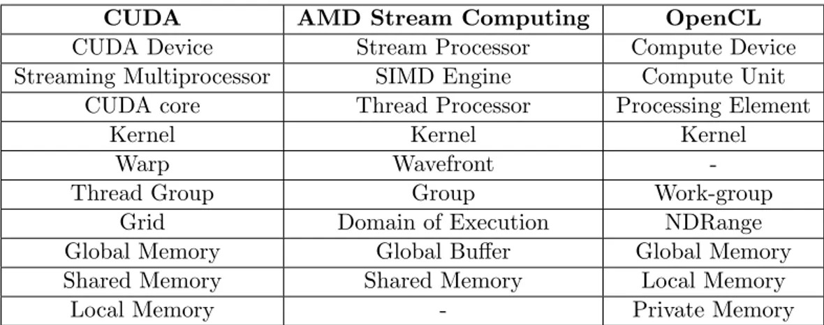
2.2.1 Nvidia Compute Unified Device Architecture . . . 20
2.2.2 AMD Stream Computing . . . 30
2.2.3 OpenCL . . . 38
2.3 Hybrid architectures . . . 44
2.4 Other existing approaches for parallelism exploitation using GPUs . . . . 44
3 Tools 47 3.1 Common Language Infrastructure . . . 47
3.1.1 Design and Capabilities . . . 47
3.1.2 Common Intermediate Language . . . 50
3.2 Common Language Runtime . . . 53
3.2.1 Reflection . . . 53
3.2.2 Metadata extensibility . . . 54
3.2.3 Delegates . . . 54
3.2.4 Managed and un-managed code . . . 56
3.2.5 Interoperating with un-managed code . . . 56
3.3 Shared Source Common Language Infrastructure . . . 58 9
3.4 CLIFile Reader . . . 59
4 Performance Modeling for GPGPU and CPU 61 4.1 Parameters for performance evaluation . . . 61
4.2 GPGPU Performance Model . . . 63
4.2.1 Related works . . . 64
4.2.2 Ground Model . . . 64
4.2.3 Refinement Example: Nvidia PTX 1.x . . . 66
4.2.4 Experimental Evaluation . . . 69
4.3 CPU Performance Model . . . 76
4.3.1 SSCLI Just-In-Time compiler . . . 76
4.3.2 Opcodes cost . . . 79 4.3.3 Experimental Evaluation . . . 80 5 Implementation 83 5.1 4-Centauri . . . 83 5.2 Libra.Net . . . 86 5.2.1 Bytecode Analysis . . . 86 5.2.2 Model Implementation . . . 89 5.2.3 Executing a task . . . 91 5.2.4 Evaluation . . . 92
6 Conclusions and Future Works 101
A Tables 105
B Listings 117
Introduction
In 1966, Micheal J. Flynn proposed a classification of computer architectures based upon the number of concurrent instructions and data streams available in the architec-ture. Flynn recognized four classes of computer architectures: Single Instruction Single Data (SISD), Single Instruction Multiple Data (SIMD), Multiple Instruction Single Data (MISD) and Multiple Instruction Multiple Data (MIMD). General-purpose architectures are architectures not devoted to a unique usage while special-purpose architectures are architectures devoted to a specific task. Generally, general-purpose architectures em-brace the Von Neumann computational model while special-purpose architectures adopt non-Von Neumann computational models. The Von Neumann computational model cor-responds to the SISD architecture in which a single processor, a uniprocessor (CPU), executes a single instruction stream, to operate on a single data stream. SIMD architec-tures exploit instead data parallelism in which multiple data elements of a stream are operated by a single instruction. For instance, Graphics Processing Units (GPUs) are SIMD architectures because graphics rendering often applies the same function to each pixel or vertex. MISD architectures apply multiple instructions on a single data stream. These are, for example, architectures used for fault tolerance or heterogeneous systems operating on the same stream element that must agree on the result. An example of MIMD architectures are distributed systems either with shared memory and distributed memory [1, 2].
GPUs have recently evolved from fixed-function rendering devices into highly par-allel programmable many-core architectures fulfilling the enormous demand for high-definition 3D games. The computational power of GPUs is available and inexpensive.A typical latest-generation card costs $400–500 at release and drops rapidly as new hard-ware emerges. As today’s computer systems often include CPUs and GPUs it is im-portant to enable software developers to take full advantage of these heterogeneous processing platforms [3].
For this reasons, many researchers and developers have become interested in harness-ing the power of commodity graphics hardware for general-purpose computharness-ing. Initially, development of non-graphics applications on GPUs was very complex because
mers had to be expert in two domains: the application domain and computer graphics. Developers had to map their applications onto the computer graphics domain specific language and code and decode respectively input and output results. Recent years have seen an explosion in interest in such research efforts, known collectively as GPGPU computing (General-Purpose GPU) [4]. The term GPGPU was coined by Mark Harris in 2002 when he recognized an early trend of using GPUs for non-graphics applica-tions [5]. Since 2005, the two major GPU vendors, Nvidia and AMD, have introduced fully programmable GPUs and development platforms such as Nvidia Compute Unified Device Architecture [6] and AMD Stream Computing [7]. GPGPU devices operate as co-processors to the main CPU, or host. More precisely, a portion of an application that drives the computation of each core is commonly known as a shader (in the traditional 3D terminology) or kernel (a term to stress the will to go beyond 3D graphics) [8]. An entire application is referred to as task. However, due to the special usage of GPU, it is impossible to complete all computing tasks solely on the GPU. Many control and serial instructions still need to complete on the CPU [9]. Despite this new interest in GPGPU computing, few efforts has been done by researchers in formulating performance models (cost models) in order to accurately evaluate performance of GPGPU applications and compare CPU executions with GPU ones of the same task.
In the last few years, researchers have become interested in Virtual Execution Envi-ronments (VEEs) such as the Java Virtual Machine (JVM) [10] and the .NET Common Language Runtime (CLR) [11]. VEEs abstract from many features of the underlying architecture through dynamic translation of code before its execution on the host. Pro-grams are expressed in an Intermediate Language (IL) and executed using an abstract computational model. Moreover, VEEs provide a specification in which code is mixed with metadata. Metadata permits to monitor program activities enforcing security, and enables dynamic loading and reflection. An important technique related to metadata is annotation: elements of source code such as classes, methods and fields can be annotated with special attributes. Attributes are compiled and saved with IL code but are ignored by the runtime. Using reflection programmers can retrieve such attributes and change programs behavior.
This thesis focuses on identifying bottlenecks in GPGPU computations through per-formance modeling. Moreover, we would like to find out if such bottlenecks could de-crease performance of parallel applications in a way that the CPU execution time of those applications become lower than the GPU one. In particular, we will focus on the overhead introduced by data transfers between host and device and the available techniques that may reduce their impact on performance. We would like to hide to developers who write parallel applications more architectural details as possible such as the number of cores and the memory bandwidth. In order to achieve better productivity, developers should be able to write parallel applications without learning GPGPU pro-gramming languages and APIs. For this reason, we leveraged the abstraction power of Virtual Execution Environments. In particular, our work enables programmers to write kernels as annotated methods using one of the available high-level languages supported by the Common Language Infrastructure (CLI) [12]. These kernels may be scheduled
on a CPU or on a GPU. In the latter case, kernels written in Microsoft Intermediate Language (MSIL) must be compiled into a target architecture language (e.g. AMD IL [7] and Nvidia PTX [6]).
In this thesis we developed Libra.Net, a single task scheduler for a CPU-GPU het-erogeneous environment. Libra.Net is written in C# using the .NET Framework and schedules tasks written in MSIL. In order to enable the scheduler to estimate the exe-cution time of a task on a CPU and on a GPU, we formulated a CPU and a GPGPU performance model. If the CPU execution time of a task is lower than the GPU one, the scheduler executes the task on the CPU, otherwise the task is executed on the GPU. Libra.Net is a component of the 4-Centauri meta-compiler, a source-to-source compiler developed by Cristian Dittamo during his PhD that translates Microsoft Intermediate Language into Nvidia PTX code [8]. During his thesis, Giacomo Righetti extended the 4-Centauri compiler with translation from MSIL to AMD IL [13]. Libra.Net performs the following steps:
• Takes in input a Kernel-annotated method.
• Analyzes the method code statically in order to estimate the number of instructions that will be executed at runtime.
• Decides on which platform execute the kernel basing on our CPU and GPGPU performance models. If the scheduler decides to execute the task on a GPGPU, 4-Centauri provides compilation from MSIL to the target architecture language. • Executes the kernel.
This thesis is organized in four chapters. In Chapter 2 we give a brief introduc-tion to the evoluintroduc-tion of GPUs that has brought to GPGPU computing. Moreover, we present and compare the main aspects of the three most spread GPGPU platforms: Nvidia CUDA [6], AMD Stream Computing [7] and OpenCL [3]. Finally, we introduce some hybrid architectures that tries to merge Von Neumann and non-Von Neumann architectures and other solutions to parallel exploitation using GPUs.
In Chapter 3 we describe design and capabilities of the Common Language Infras-tructure and we briefly introduce the techniques of the Common Language Runtime used for the scheduler implementation.
In Chapter 4 we propose a GPGPU performance model structured in layers. The abstract layer (we called the “ground model”) is a performance model based on the OpenCL platform and specification. We chose OpenCL because it is an open standard. Moreover it is supported by the two major graphics card vendors (Nvidia and AMD). The ground model must be refined to produce a performance model tied to a vendor-specific platform or even to a vendor-specific device. In particular, we propose a refinement of the ground model that is tied to the Nvidia PTX 1.x platform.
In order to compare CPU and GPU execution times we formulated a simple CPU performance model. Our model is based on the computational model of the CLI virtual
execution environment. Virtual execution environments abstract from specific underly-ing architecture features makunderly-ing their sequential execution model well-suited for perfor-mance modeling. Moreover, virtual execution environments enable programs to inspect their code at runtime through Metadata and Reflection. These techniques are useful to infer a program behavior. We corroborated the GPGPU and the CPU performance models through an experimental approach. We set up several tests in order to compare experimental and theoretical results.
Finally, in Chapter 5 we present the main implementation aspects of Libra.Net and evaluate its efficiency in two case study applications: a Vector Addition and a Matrix Multiplication.
State of the Art
In this chapter we give an introduction to the major hardware and software innovations that brought from first generation special-purpose graphics cards to modern General-Purpose Graphics Processing Units (GPGPUs). Then we present the programming model, memory model and communication model of the three main GPGPU platforms. Finally, we give a brief description of the new CPU-GPU hybrid architectures and other approaches for parallel exploitation using GPUs.
2.1
Evolution of the Graphics Processing Unit
To make this thesis self-contained, in the following sections we present the hardware and software evolution of graphics processing units which has led to GPGPU computing. We identify four main GPU generations: fixed-function graphics pipeline, programmable shading, programmable graphics and GPGPU (Figure 2.1) [14]. This is a simplified
Figure 2.1: Evolution of the Graphics Processing Unit.
view of the evolution of the GPU. Other minor software and hardware improvements should be placed between the four macro-steps but this is out of our interest.
The graphics pipeline1, also called rendering pipeline, is a method of rasterization-based rendering implemented by graphics cards. The graphics pipeline accepts as input a representation of a three-dimensional scene and outputs a 2D image that can be displayed
1
In computing, a pipeline is a set of data processing elements connected in series, so that the output of one element is the input of the next one. The elements of a pipeline are often executed in parallel or in time-sliced fashion.
on a screen. A generic 3D application provides a representation of a scene in the form of vertices that can be manipulated in parallel by the steps composing the graphics pipeline [15]. Figure 2.2 depicts a simplified model of the graphics pipeline.
Figure 2.2: The graphics pipeline.
2.1.1 Fixed-function Graphics Pipeline
First generation graphics cards (1996-1999) implemented a hardware-coded fixed-function graphics pipeline (Figure 2.3) i.e. there was a specialized (not programmable) hardware unit for each step composing the pipeline. In OpenGL 1.x [16] and DirectX 9 [17] a little “customization” was possible through parameters setting.
Figure 2.3: Fixed-function graphics pipeline.
2.1.2 Programmable Shading
From 2001, major graphics software libraries such as OpenGL [16] and Direct3D (compo-nent of the DirectX API [17]) began to enable programmers to define special functions, called shaders, to be executed by GPUs. The beginning of shaders marked the transition from a fixed-function pipeline to a programmable one as depicted in Figure 2.4. Shaders
Figure 2.4: Programmable shading.
replace fixed-functions composing the rendering pipeline in order to obtain customized graphic effects such as bump mapping and color toning [15].
Shader programs can be written using a shading language (i.e. a Domain Specific Language) such as the OpenGL Shading Language (GLSL) [16], the High Level Shader Language (HLSL) [11] from Microsoft or Cg (C for graphics) [18] developed by Nvidia in collaboration with Microsoft.
2.1.3 Programmable Graphics
A major innovation in graphics shaders, introduced by DirectX 10 in 2006, was of the Unified Shader Model which consists of two aspects: the Unified Shader Model and the Unified Shader Architecture. The Unified Shader Model (known in OpenGL simply
Figure 2.5: Unified shader model.
consists in defining a very similar instruction set for all shader types. The Unified Shader Architecture is a low-level model that “unifies” the GPU compute units meaning that any of them can run any type of shader. Hardware is not required to have a Unified Shading Architecture to support the Unified Shader Model, and vice versa. With the Unified Shader Model the graphics pipeline become fully programmable. The graphics pipeline steps can be replaced, added and ordered by programmers (Figure 2.5) [20].
2.1.4 General Purpose GPU
The advance from the Unified Shader Model to GPGPU computing mainly consists in a change of the provided programming interfaces and languages rather than on hardware modifications. It has passed from Domain Specific Languages (shading languages) to general-purpose programming languages such as C, FORTRAN, etc. The hardware design has substantially remained the same, just more transistors have been placed on a chip following a trend in which the number of transistors doubles every six months. Since modern GPGPUs still implement a SIMD architectural model, speaking about “general-purpose” architectures would be incorrect. In fact, as it will be explained in this thesis, not all kinds of applications are well-suited to be executed on a GPU but only those that can fit the data-parallellism programming model. The “general-purpose” term has been introduced in order to emphasize the new capability of GPUs of executing non-graphics applications. Lots of algorithms belonging for example to the fields of physics simulation and computational biology can be accelerated by data parallel implementations making them well-suited for the execution on GPGPUs.
The GPGPU computational model exposes to programmers a stream processing paradigm. Stream processing is a computer programming paradigm, related to SIMD, that allows some applications to more easily exploit a limited form of parallel process-ing. The stream processing paradigm restricts the parallel computation that can be performed by parallel software and hardware. Given a set of data (a stream), a series of operations (kernel functions) are applied to each element in the stream. Shaders and kernels have the same meaning. The name has been changed just to stress the the will to go beyond 3D graphics.
The following example explains the GPGPU programming model using pseudo-code. Listing 2.1 shows a sequential implementation of the matrix sum.
void sum ( f l o a t A [ ] , f l o a t B [ ] , f l o a t C [ ] ) { f o r ( i n t i = 0 ; i < n ; i ++) { f o r ( i n t j = 0 ; j < m; j ++) { C [ i ] [ j ] = A [ i ] [ j ] + B [ i ] [ j ] ; } } }
This code can be executed sequentially on a CPU such that C[0][1] is computed after C[0][0] and so on. However, the elements of C can be calculated independently by a number of threads equals to the size of each matrix. Listing 2.2 shows a multi-threaded version of the same application.
void sum ( f l o a t A [ ] , f l o a t B [ ] , f l o a t C [ ] ) { f o r ( i n t i = 0 ; i < n ; i ++) { f o r ( i n t j = 0 ; j < m; j ++) { l a u n c h t h r e a d { C [ i ] [ j ] = s u m k e r n e l ( i , j , A, B) ; } } } s y n c h t h r e a d s ( ) ; }
Listing 2.2: Multi-threaded version of the sum of two matrices.
The function sum_kernel() can represent the kernel of an hypothetical GPGPU application that performs the sum of two matrices. In this case threads are mapped onto the elements of matrix C, that is each thread is assigned a single element of the output matrix (one-to-one mapping). In a parallel environment the nested “for” loops are simulated by the hardware. Programmers must thus provide the kernel function, the input and output buffers and the type of mapping. The runtime will correctly map threads to cores of the underlying architecture [7].
2.2
GPGPU platforms
The following sections describe the programming model of the three main GPGPU plat-forms: Nvidia Compute Unified Device Architecture [6], AMD Stream Computing [7] and OpenCL [3]. Since our aim is to introduce the GPGPU computational model and not to present all the available GPGPU platforms, other solutions will be cited at the end of this chapter.
2.2.1 Nvidia Compute Unified Device Architecture
Nvidia Compute Unified Device Architecture (CUDA) is a general purpose parallel com-puting architecture developed and introduced by Nvidia in November 2006. CUDA pro-vides a new Instruction Set Architecture (ISA) and a new parallel programming model enabling programmers to solve non-graphics computational problems using its GPUs. A software environment that uses C as the primary high-level programming language is given to developers. Other programming languages are going to be supported by CUDA such as FORTRAN [6].
Programming Model
The CUDA programming model assumes that CUDA threads execute on a physically separate device that operates as a coprocessor to the host running the C program. Moreover, the CUDA programming model assumes that both the host and the device maintain their own separate memory spaces in RAM (Random Access Memory), referred to as host memory and device memory, respectively. CUDA programs manage device memory through calls to the CUDA runtime. This includes device memory allocation and deallocation as well as data transfer between host and device memory [6].
When an application launches a kernel, an user-specified number of threads are created and scheduled for the execution. Threads execute the same kernel function. Each thread executing the kernel has a unique identifier. Threads can be grouped in one-dimensional, two-dimensional or three-dimensional thread blocks. Thread blocks are themselves organized in a one-dimensional or two-dimensional grid as illustrated in Figure 2.6. For each kernel, a single grid of threads can be launched. The number of thread blocks per grid is dictated by the size of the data being processed. Precisely, the grid size is obtained dividing data size by block size [6].
Programming Interface. The two main programming interfaces provided by CUDA are CUDA C and CUDA Driver API. CUDA C is a small extension to the C language syntax. CUDA Driver API is a low-level interface that enables programmers to gain more control over kernel execution but is harder to program and debug. CUDA C is essentially built on top of the CUDA Driver API, hiding to programmers low-level operations such
Figure 2.6: The CUDA thread hierarchy.
as runtime initialization and management. CUDA C provides extensions to the standard C syntax enabling developers to define kernel functions.
For instance, kernels are declared with the __global__ declaration specifier and have access to some built-in variables. Programmers configure a kernel launch through the <<< ... >>> configuration syntax specifying, for example, block size and grid size. The thread identifier is accessible through threadIdx built-in variable that is a triple in which the components represent the coordinates of the thread inside its thread block. The blockIdx built-in variable is a 2-component vector that contains the block index within its grid. The dimension of each block is accessible through the blockDim built-in variable [6].
Listing 2.3 [21] shows a kernel function that uses the three different built-in variables presented above to perform the saxpy function, a combination of scalar multiplication and vector addition. CUDA functions such as cudaMallocHost(), cudaMalloc() and cudaMemcpy() will be explained further in this chapter when we will speak about the CUDA communication model (Section 2.2.1).
g l o b a l void Saxpy ( f l o a t a , f l o a t ∗ InData1 , f l o a t ∗ InData2 , f l o a t ∗ R e s u l t ) { i n t i d x = b l o c k I d x . x ∗ blockDim . x + t h r e a d I d x . x ; R e s u l t [ i d x ] = InData1 [ i d x ] ∗ a + InData2 [ i d x ] ; } i n t main ( i n t a r g c , char ∗∗ a r g v ) { f l o a t ∗ I n i t D a t a 1 , ∗ I n i t D a t a 2 , ∗ InData1 , ∗ InData2 , ∗ R e s u l t , ∗ H o s t R e s u l t ; f l o a t a = 1 0 . 0 ; unsigned i n t Length = 1 0 0 ; /∗ −−−−−−− MEMORY ALLOCATION −−−−−−−− ∗/
c u d a M a l l o c H o s t ( ( void ∗ ∗ )&H o s t R e s u l t , Length ) ; memset ( H o s t R e s u l t , 0 , Length ) ;
c u d a M a l l o c ( ( void ∗ ∗ )&InData1 , s i z e o f ( f l o a t ) ∗ Length ) ; c u d a M a l l o c ( ( void ∗ ∗ )&InData2 , s i z e o f ( f l o a t ) ∗ Length ) ; c u d a M a l l o c ( ( void ∗ ∗ )&R e s u l t , s i z e o f ( f l o a t ) ∗ Length ) ;
/∗ −−−−−−− SET INPUT VALUES −−−−−−−− ∗/
I n i t D a t a 1 = ( f l o a t ∗ ) m a l l o c ( s i z e o f ( f l o a t ) ∗ Length ) ; I n i t D a t a 2 = ( f l o a t ∗ ) m a l l o c ( s i z e o f ( f l o a t ) ∗ Length ) ; f o r ( i n t i = 0 ; i < Length ; ++i ) { I n i t D a t a 1 [ j ] = ( f l o a t ) rand ( ) ; I n i t D a t a 2 [ j ] = ( f l o a t ) rand ( ) ; }
cudaMemcpy ( InData1 , I n i t D a t a 1 , s i z e o f ( f l o a t ) ∗ Length , cudaMemcpyHostToDevice ) ; cudaMemcpy ( InData2 , I n i t D a t a 2 , s i z e o f ( f l o a t ) ∗ Length , cudaMemcpyHostToDevice ) ;
/∗ −−−−−−− RUN COMPUTE KERNEL −−−−−−−− ∗/
i n t n = 16 ∗ 1024 ∗ 1 0 2 4 ; dim3 t h r e a d s = dim3 ( 5 1 2 , 1 ) ;
dim3 b l o c k s = dim3 ( n / t h r e a d s . x , 1 ) ;
Saxpy<<<b l o c k s , t h r e a d s , 0>>>(a , InData1 , InData2 , OutData ) ;
/∗ −−−−−−− GET RESULT −−−−−−−− ∗/
cudaMemcpy ( H o s t R e s u l t , R e s u l t , s i z e o f ( f l o a t ) ∗ Length , cudaMemcpyDeviceToHost ) ; }
Listing 2.3: CUDA implementation of the saxpy function.
Thread blocks execute independently, that is they can be executed in any order, in parallel or in series. It is, therefore, possible to schedule thread blocks in any order across any number of cores enabling programmers to write code that scales with the number cores. Threads within a block can share data using the on-chip shared memory region and synchronize memory accesses through the __synchthreads() function that acts as a barrier at which all threads in a block must wait before any is allowed to proceed.
Compilation tool-chain. The CUDA compilation tool-chain is composed of three stages as depicted in Figure 2.7. Kernels are compiled with nvcc [22](the compiler provide by Nvidia) in an intermediate language called PTX [23] (Parallel Thread eXe-cution). PTX is the Nvidia low-level virtual machine and ISA designed to support the operations of a parallel CUDA processor.
Figure 2.7: CUDA’s compilation process.
code to be executed on the host) from device code (i.e. code to be executed on the device). Host code can be compiled using nvcc or another tool chosen by the programmer. Source code written for the host CPU follows a fairly traditional path and allows developers to choose their own C/C++ compiler. During the second stage, device code is compiled into PTX and/or in a binary form (cubin object). The second stage is performed by the Nvidia’s PTX-to-Target Translator, which converts Open64’s assembly-language output into executable code for specific Nvidia GPUs [24]. An application can link to the generated device code, i.e. the PTX or the cubin, or load and execute the kernel at runtime using just-in-time compilation. Just-in-time compilation increases application load time but benefits from latest compiler improvements. Moreover this technique permits the execution of an application on different devices without recompilation.
Nvidia and the Portland Group (component of STMicroelectronics) has recently announced their collaboration on CUDA x86 [25], a solution that enables CUDA appli-cations to be executed on any PC system or server. The PGI CUDA C x86 compiler enables programmers to optimize CUDA applications for their execution on x86 systems not equipped with Nvidia graphics cards.
Memory Model
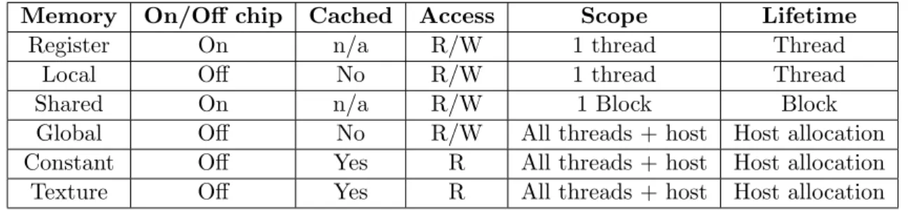
CUDA threads can access and share several memory spaces at different levels during a kernel execution (Figure 2.8):
• Registers. A set of 32-bit registers located on-chip. Each thread can access a private subset of the available registers.
CUDA C Programming Guide Version 3.1 11
Figure 2-2. Memory Hierarchy
2.4 Heterogeneous Programming
As illustrated by Figure 2-3, the CUDA programming model assumes that the CUDA threads execute on a physically separate device that operates as a coprocessor to the host running the C program. This is the case, for example, when the kernels execute on a GPU and the rest of the C program executes on a CPU.
Global memory Grid 0 Block (2, 1) Block (1, 1) Block (0, 1) Block (2, 0) Block (1, 0) Block (0, 0) Grid 1 Block (1, 1) Block (1, 0) Block (1, 2) Block (0, 1) Block (0, 0) Block (0, 2) Thread Block Per-block shared memory Thread Per-thread local memory
Figure 2.8: The CUDA memory spaces [6].
• Local Memory. A memory region with a scope local to a thread. Local does not mean physically close to the cores in which threads executes. In fact this memory region is located off-chip on a partition of the GPU RAM. Accessing this memory region is as expensive as accessing global memory. Moreover, like global memory, local memory is not cached. Local memory is only used by the nvcc compiler to hold automatic variables that can not be saved in registers. Programmers can access this memory space only developing at the lowest level provided by Nvidia (PTX ISA).
• Shared Memory. An user-managed cache located on-chip that is shared between threads in a block. Shared memory is a limited resource (16 Kb). Like registers, if not enough space is available, considering threads memory requirements, a kernel is not launched and an error is reported. The shared memory is divided into equally sized modules, called banks. Accessing shared memory is as fast as accessing registers. However, if different requests from different threads addresses the same bank (called bank conflict ), the accesses are serialized decreasing bandwidth and performance.
• Global Memory. This memory region is located inside the GPU RAM. It is shared between all threads in a grid and across multiple kernel launches of the same CUDA application. Input and output data are allocated in global memory to be
transferred respectively from and to the host memory. Accessing this memory region is very expensive and could be a bottleneck for kernel performance.
• Constant Memory. There is a total of 64 KB constant memory on a device. The constant memory space is cached. As a result, a read from constant memory costs one memory read from device memory only on a cache miss; otherwise, it just costs one read from the constant cache.
• Texture Memory. The read-only texture memory space is cached. Therefore, a texture fetch costs one device memory read only on a cache miss; otherwise, it just costs one read from the texture cache. The texture cache is optimized for 2D spatial locality, so threads reading texture addresses that are close together will achieve best performance.
Table 2.1 lists the CUDA memory spaces and their features.
Memory On/Off chip Cached Access Scope Lifetime
Register On n/a R/W 1 thread Thread
Local Off No R/W 1 thread Thread
Shared On n/a R/W 1 Block Block
Global Off No R/W All threads + host Host allocation Constant Off Yes R All threads + host Host allocation Texture Off Yes R All threads + host Host allocation
Table 2.1: Salient features of CUDA device memory spaces.
Coalesced and un-coalesced global memory accesses. Coalesced memory access is a memory access mechanism that is able to considerably increase the overall per-formance of an application [26]. Global memory operations issued by threads can be batched into a single memory transaction when certain requirements are met. Detailed information about coalescing requirements are provided by the CUDA documentation [6]. If a memory access pattern does not fulfill these requirements, a separate transaction results for each requested element (un-coalesced memory accesses).
Hardware Model
CUDA devices are composed of a scalable array of Streaming Multiprocessors (SMs) as illustrated in Figure 2.9. Each SM contains a fixed number (typically 8) of Stream Processor (or CUDA cores). Each SP has a fully pipelined integer arithmetic logic unit (ALU) and floating point unit (FPU). A CUDA core executes a floating point or integer instruction per clock for a thread.
Figure 2.9: CUDA Hardware Architecture.
An SM executes hundreds of threads concurrently in a SIMT2 (Single-Instruction Multiple-Thread) fashion. The SMs schedule threads in groups of 32 threads called warps that are the unit of parallelism. All threads in a warp execute the same instruction at the same time but they are free to take different execution paths in case of a branch divergence. If threads diverge for a data-dependent conditional branch the paths are executed in series and when all paths are completed the warp converge back to the same instruction. Branch divergence can occur only within a warp, different warps can execute independently and take different execution paths. Full efficiency is reached when all threads within a warp agree on their execution path [6].
When a kernel is launched, threads of a grid are enumerated and distributed to the SMs for the execution. Each SM is assigned a set of thread blocks that are executed sequentially. Thread blocks are partitioned into warps that are scheduled by the warp scheduler. The partitioning is always the same: each warp contains thread of consecutive thread IDs with the first warp containing thread 0 [27].
The execution information of a warp such as the program counter and the registers content are maintained on-chip during the entire lifetime of the warp. Therefore the context switch has no cost because the scheduler select a ready warp (i.e. a warp that contains active threads or equivalently a warp that does not contain threads waiting for
2The SIMT architecture is akin to SIMD. A key difference is that SIMD vector organizations expose
the SIMD width to the software, whereas SIMT instructions specify the execution and branching behavior of a single thread. In contrast with SIMD vector machines, SIMT enables programmers to write thread-level parallel code for independent, scalar threads, as well as data-parallel code for coordinated threads.
a memory response) and simply issues the next instruction for that warp.
Compute Capability. The compute capability is a revision number that specifies features and capabilities of a device. It is defined by a major revision number and a minor revision number. Devices with the same major revision number are of the same core architecture. The major revision number of devices based on the Fermi architecture is 2. Prior devices are all of compute capability 1.x (their major revision number is 1). The minor revision number corresponds to an incremental improvement to the core architecture, possibly including new features [6].
Communication Model
The typical steps involved in the execution of a CUDA application are illustrated in Figure 2.10. First of all input data are transferred from host memory to device memory through the PCIe bus. When data transfer is completed, the host instructs the device to start processing and the computation take place onto the device cores in parallel. Finally, results are copied back from the device memory to the host memory to be post-processed.
Figure 2.10: Example of CUDA processing flow.
Data transfers between host memory and device memory can be bottlenecks in GPGPU computations because the peak bandwidth of the PCIe bus is almost an order of magnitude lower than the peak bandwidth between the device memory and the device chip. Hence, to achieve the best performance, it is fundamental to
• batch many small transfers into a single larger transfer for reducing the overhead introduced by the bus and buffer management;
• increase transfer bandwidth allocating buffers in page-locked host memory; • overlapping computation and data transfers. This technique is not available on all
CUDA devices and depends on the compute capability.
Page-Locked Host Memory. Page-locked host memory, also known as pinned mem-ory, is a region of the host memory that, in spite of pageable memmem-ory, is not swapped to secondary storage. The main advantages using page-locked host memory are:
• Copies between page-locked host memory and device memory can be performed concurrently with kernel execution for some devices.
• On systems with a front-side bus, bandwidth between host memory and device memory is higher if host memory is allocated as page-locked.
However, pinned memory is a limited resource. Allocating too much data in this memory space reduces the physical memory available for the operating system decreasing overall performance.
Overlapping computation and data transfers. Host to device data transfers are generally blocking transfers meaning that control is returned to the host thread only after all data has been transferred. However it is possible to overlap host computation and memory transfers through asynchronous calls in which control is returned immediately to the host thread. Asynchronous data transfers functions contain an additional parameter that represents the stream. A stream is a sequence of operations that are performed in order by a device. Listing 2.4 shows how to execute the cpuFunction() while some data is transferred to the device and the kernel is executed on the device.
cudaMemcpyAsync ( a d , a h , s i z e , cudaMemcpyHostToDevice , 0 ) ; a K e r n e l <<<g r i d , b l o c k >>>(a d ) ;
c p u F u n c t i o n ( ) ;
Listing 2.4: Overlapping host computation and data transfers.
In this case the memory transfer is associated to the stream 0 that is the default stream. The kernel also uses the stream 0 so it will not start until the transfer will be completed. Some devices have the capability of overlapping memory transfers and kernel execution simply assigning different streams to each operation as shown in Listing 2.5. Obviously, the computation must have data dependencies that permit the partitioning of data in chunks that can be manipulated independently by different kernels [27].
s i z e = N∗ s i z e o f ( f l o a t ) / nStreams ; f o r ( i = 0 ; i < nStreams ; i ++) {
o f f s e t = i ∗N/ nStreams ;
cudaMemcpyAsync ( a d+o f f s e t , a h+o f f s e t , s i z e , d i r , s t r e a m [ i ] ) ; }
f o r ( i = 0 ; i < nStreams ; i ++) { o f f s e t = i ∗N/ nStreams ;
a K e r n e l <<<N/ ( nThreads ∗ nStreams ) , nThreads , 0 , s t r e a m [ i ]>>>( a d+ o f f s e t ) ; }
Listing 2.5: Concurrent copy and kernel execution.
Nvidia GF100
The Nvidia GF100 processor, code named “Fermi” [28], is the new core architecture from Nvidia that comes with many improvements on the preceding CUDA architecture. The new Fermi SMs contains 32 CUDA cores, four times the number of cores in preceding CUDA architectures. A Streaming Multiprocessor is able now to execute two warps concurrently thanks to the Dual Warp Scheduler, two Instruction Dispatch Units and the amount of CUDA cores. With Fermi, the amount of shared memory per SM has
Figure 2.11: On the left is represented the serial kernel execution prior to Fermi, while on the right is represented the concurrent kernel execution available on Fermi.
been increased to 64 Kb that can be configured as 48 Kb of shared memory and 16 Kb of L1 cache or 16 Kb of shared memory and 48 Kb of L1 cache. In addition to the L1 cache, Fermi features a 768 Kb unified L2 cache that services all load, store and texture requests. Fermi is the first architecture that support PTX 2.0 instruction set. Support to C++ has been obtained with the implementation of a unified address space that unifies the three previously separated address spaces (local memory, shared memory, global memory). Moreover, creation and deletion of objects, exception handling and function pointers are now supported. The application context switch on the GPU has been improved for better kernel-to-kernel communication performance. Fermi supports concurrent kernel execution for kernels of the same application (Figure 2.11). This allows many small kernels to be executed concurrently on the GPU without waste of resources.
2.2.2 AMD Stream Computing
AMD Stream Computing is a programming model and an hardware architecture that enables GPGPU computing over AMD GPUs.
Programming Model
Kernels are executed in parallel using a virtualized SIMD programming model by the GPU hardware. Instances of a kernel running on the GPU are called threads. Threads of the same kernel execution are grouped together forming the domain of execution and mapped to the elements of the output buffer. A group is a set number of threads that execute blocks of code together in parallel before another group can execute the same block of code. The current generation of AMD GPUs allows threads within a single group to share data and synchronize with each other. This can be useful in certain applications where inter-thread communication is either vital to the algorithm or can vastly speedup the execution of the application [7].
Programming Interface. Programmers developing GPGPU applications on AMD devices can choose between two programming interfaces: AMD Brook+ and AMD Com-pute Abstraction Layer (CAL) [7]. Brook+ is a data-parallel C compiler that extends the ANSI C programming language with two main key elements: streams and kernels. Kernels are declared using the kernel declaration specifier while streams are specified through the <> syntax. Each thread can obtain its identifier within its group calling the instanceGroup() function while its identifier inside the entire domain of execution can be obtained through the instance() function. Group size can be specified using Attribute[GroupSize (x, y, z)]. Threads in a group can synchronize their execu-tion and memory accesses calling the syncGroup() funcexecu-tion. When all threads in a group have reached the synchronization barrier, the execution of each thread can con-tinue from that point. Listing 2.6 [21] shows a Brook+ application that performs the saxpy function.
kernel void Saxpy ( f l o a t a , f l o a t x<>, f l o a t y<>, out f l o a t r e s u l t <>) { r e s u l t = a ∗ x + y ; } i n t main ( i n t a r g c , char ∗∗ a r g v ) { unsigned i n t Length = 1 0 0 ; f l o a t a = 1 0 . 0 ; f l o a t ∗ InData1 ; f l o a t ∗ InData2 ; f l o a t ∗ R e s u l t ; /∗ −−−−−−− MEMORY ALLOCATION −−−−−−−− ∗/ InData1 = ( f l o a t ∗ ) m a l l o c ( s i z e o f ( f l o a t ) ∗ Length ) ; InData2 = ( f l o a t ∗ ) m a l l o c ( s i z e o f ( f l o a t ) ∗ Length ) ; R e s u l t = ( f l o a t ∗ ) m a l l o c ( s i z e o f ( f l o a t ) ∗ Length ) ;
/∗ −−−−−−− SET INPUT VALUEs −−−−−−−− ∗/
f o r ( i n t i = 0 ; i < Length ; ++i ) { InData1 [ i ] = ( f l o a t ) rand ( ) ; InData2 [ i ] = ( f l o a t ) rand ( ) ; } /∗ −−−−−−− SET DOMAIN −−−−−−−− ∗/ f l o a t i n d a t a 1 <Length >; f l o a t i n d a t a 2 <Length >; f l o a t r e s u l t <Length >; streamRead ( i n d a t a 1 , InData1 ) ; streamRead ( i n d a t a 2 , InData2 ) ;
/∗ −−−−−−− RUN COMPUTE KERNEL −−−−−−−− ∗/
Saxpy ( a , InData1 , InData2 , OutData ) ;
/∗ −−−−−−− GET RESULT −−−−−−−− ∗/
s t r e a m W r i t e ( OutData , r e s u l t ) ;
/∗ −−−−−−− CLEAN UP and EXIT −−−−−−−− ∗/
f r e e ( InData1 ) ; f r e e ( InData2 ) ; f r e e ( R e s u l t ) ; return 0 ; }
Listing 2.6: Brook+ implementation of the saxpy function.
Comparing Listing 2.3 and Listing 2.6 we note many similarities between the CUDA and the AMD Stream Computing programming model: input data initialization, allocation and copy into the device memory, kernel launch and copy of output data from device memory to host memory.
CAL is a device driver library used by programmers to write kernels at a lower level and to gain more control over kernel execution. CAL runtime accepts kernels written in AMD IL and produces executable code for the target architecture. Listing 2.7 [21] shows a CAL application that performs the saxpy function. Code in Listing 2.6 and Listing 2.7 perform the same kernel launch. However, the latter requires a number of code lines
that is almost three times that of the former. Moreover, CAL programmers must have a better understanding of the underlying hardware architecture [7].
const CALchar∗ I L k e r n e l = “ i l p s 2 0 \ n” “ d c l i n p u t p o s i t i o n i n t e r p ( l i n e a r n o p e r s p e c t i v e ) v0 . x y \ n” “ d c l o u t p u t g e n e r i c o0 . x \ n” “ d c l c b cb0 [ 1 ] \ n” “ d c l r e s o u r c e i d ( 0 ) t y p e ( 2 d , unnorm ) f m t x ( f l o a t ) f m t y ( f l o a t ) f m t z ( f l o a t ) fmtw ( f l o a t ) \ n” “ d c l r e s o u r c e i d ( 1 ) t y p e ( 2 d , unnorm ) f m t x ( f l o a t ) f m t y ( f l o a t ) f m t z ( f l o a t ) fmtw ( f l o a t ) \ n” “ s a m p l e r e s o u r c e ( 0 ) s a m p l e r ( 0 ) r0 , v0 . xyxx \ n” “ s a m p l e r e s o u r c e ( 1 ) s a m p l e r ( 0 ) r1 , v0 . xyxx \ n” “ m a d i e e e o0 . x , cb0 [ 0 ] . x , r 0 . x , r 1 . x \ n” “ r e t d y n \ n” “end \ n” ; i n t main ( i n t a r g c , char ∗∗ a r g v ) { /∗ −−−−−−− INITIALIZATION −−−−−−−− ∗/ c a l I n i t ( ) ; CALuint numDevices = 0 ; c a l D e v i c e G e t C o u n t (&numDevices ) ; C A L d e v i c e i n f o i n f o ; c a l D e v i c e G e t I n f o (& i n f o , 0 ) ; CALdevice d e v i c e = 0 ; c a l D e v i c e O p e n (& d e v i c e , 0 ) ; CALcontext c t x = 0 ; c a l C t x C r e a t e (& c t x , d e v i c e ) ;
/∗ −−−−−−− COMPILE & LINK KERNEL −−−−−−−− ∗/
C A L d e v i c e a t t r i b s a t t r i b s ;
a t t r i b s . s t r u c t s i z e = s i z e o f ( C A L d e v i c e a t t r i b s ) ; c a l D e v i c e G e t A t t r i b s (& a t t r i b s , 0 ) ;
CALobject o b j ;
c a l c l C o m p i l e (& o b j , CAL LANGUAGE IL, I L k e r n e l , a t t r i b s . t a r g e t ) ; // L i n k o b j e c t i n t o an image
CALimage image = NULL ; c a l c l L i n k (&image , &o b j , 1 ) ;
/∗ −−−−−−− MEMORY ALLOCATION −−−−−−−− ∗/
// a l l o c a t e i n p u t / o u t p u t r e s o u r c e s and map them i n t o t h e c o n t e x t unsigned i n t Length = 1 0 0 ;
CALresource InData1 = 0 ; CALresource InData2 = 0 ;
c a l R e s A l l o c L o c a l 1 D (&InData1 , d e v i c e , Length , CAL FORMAT DOUBLE 1, 0 ) ; c a l R e s A l l o c L o c a l 1 D (&InData2 , d e v i c e , Length , CAL FORMAT DOUBLE 1, 0 ) ; CALresource R e s u l t = 0 ;
c a l R e s A l l o c L o c a l 1 D (& R e s u l t , d e v i c e , Length , CAL FORMAT DOUBLE 1, 0 ) ; CALresource a = 0 ;
c a l R e s A l l o c R e m o t e 1 D (&a , &d e v i c e , 1 , 1 , CAL FORMAT DOUBLE 1, 0 ) ; CALuint p i t c h 1 = 0 , p i t c h 2 = 0 ;
CALmem InMem1 = 0 , InMem2 = 0 ;
/∗ −−−−−−− SET INPUT VALUEs −−−−−−−− ∗/
f l o a t ∗ f i n d a t a 1 = NULL ; f l o a t ∗ f i n d a t a 2 = NULL ;
calCtxGetMem(&InMem1 , c t x , InData1 ) ; calCtxGetMem(&InMem2 , c t x , InData2 ) ;
calResMap ( ( CALvoid ∗ ∗ )&f i n d a t a 1 , &p i t c h 1 , InData1 , 0 ) ; f o r ( i n t i = 0 ; i < Length ; ++i )
calResUnmap ( InData1 ) ;
calResMap ( ( CALvoid ∗ ∗ )&f i n d a t a 2 , &p i t c h 2 , InData2 , 0 ) ; f o r ( i n t i = 0 ; i < Length ; ++i ) f i n d a t a 2 [ i ∗ p i t c h 2 ] = rand ( ) ; calResUnmap ( InData2 ) ; f l o a t ∗ c o n s t P t r = NULL ; CALuint c o n s t P i t c h = 0 ; CALmem constMem = 0 ;
// Map c o n s t a n t r e s o u r c e t o CPU and i n i t i a l i z e v a l u e s calCtxGetMem(&constMem , c t x , a ) ;
calResMap ( ( CALvoid ∗ ∗ )&c o n s t P t r , &c o n s t P i t c h , a , 0 ) ; c o n s t P t r [ 0 ] = 1 0 . 0 ;
calResUnmap ( a ) ;
// Mapping o u t p u t r e s o u r c e t o CPU and i n i t i a l i z i n g v a l u e s void ∗ r e s d a t a = NULL ; CALuint p i t c h 3 = 0 ; CALmem OutMem = 0 ; calCtxGetMem(&OutMem, c t x , R e s u l t ) ; calResMap(& r e s d a t a , &p i t c h 3 , R e s u l t , 0 ) ; memset ( r e s d a t a , 0 , p i t c h 3 ∗ Length ∗ s i z e o f ( f l o a t ) ) ; calResUnmap ( R e s u l t ) ;
/∗ −−−−−−− LOAD MODULE & SET DOMAIN −−−−−−−− ∗/
CALmodule module ;
calModuleLoad (&module , c t x , image ) ; CALfunc f u n c ;
CALname InName1 , InName2 , OutName , ConstName ; c a l M o d u l e G e t E n t r y (& f u n c , c t x , module , “main” ) ; calModuleGetName(&InName1 , c t x , module , “ i 0 ” ) ; calModuleGetName(&InName2 , c t x , module , “ i 1 ” ) ; calModuleGetName(&OutName , c t x , module , “o0” ) ; calModuleGetName(&ConstName , c t x , module , “c b0 ” ) ; calCtxSetMem ( c t x , InName1 , InMem1 ) ;
calCtxSetMem ( c t x , InName2 , InMem2 ) ; calCtxSetMem ( c t x , OutName , OutMem) ; calCtxSetMem ( c t x , ConstName , constMem ) ; CALdomain domain = { 0 , 0 , Length , 1 } ;
/∗ −−−−−−− RUN COMPUTE KERNEL −−−−−−−− ∗/
CALevent e v e n t ;
calCtxRunProgram(& e v e n t , c t x , f u n c , &domain ) ; // w a i t f o r f u n c t i o n t o f i n i s h
while ( c a l C t x I s E v e n t D o n e ( c t x , e v e n t ) == CAL RESULT PENDING) { } ;
/∗ −−−−−−− GET RESULT −−−−−−−− ∗/
CALuint p i t c h 4 = 0 ; f l o a t ∗ f o u t d a t a = 0 ;
calResMap ( ( CALvoid ∗ ∗ )& f o u t d a t a , & p i t c h 4 , R e s u l t , 0 ) ; f o r ( i n t i = 0 ; i < Length ; ++i )
f o u t d a t a [ i ∗ p i t c h 4 ] = ( f l o a t ) ( i ∗ p i t c h 4 ) ; calResUnmap ( R e s u l t ) ;
/∗ −−−−−−− CLEAN UP and EXIT −−−−−−−− ∗/
c a l M o d u l e U n l o a d ( c t x , module ) ; c a l c l F r e e I m a g e ( image ) ; c a l c l F r e e O b j e c t ( o b j ) ; calCtxReleaseMem ( c t x , InMem1 ) ; c a l R e s F r e e ( InData1 ) ; calCtxReleaseMem ( c t x , InMem2 ) ; c a l R e s F r e e ( InData2 ) ; calCtxReleaseMem ( c t x , constMem ) ;
c a l R e s F r e e ( a ) ; calCtxReleaseMem ( c t x , OutMem) ; c a l R e s F r e e ( R e s u l t ) ; c a l C t x D e s t r o y ( c t x ) ; c a l D e v i c e C l o s e ( d e v i c e ) ; calShutdown ( ) ; }
Listing 2.7: AMD CAL implementation of saxpy function.
Compilation tool-chain. The software stack that provides compilation of Brook+ files (.br) is illustrated in Figure 2.12. brcc is a source-to-source meta compiler that takes a .br file and separates code to be executed on the CPU from code to be executed on the GPU. The former is compiled into the host machine code while the latter is compiled into AMD IL (i.e. the AMD ISA). brt is a run-time library able to call device
Figure 2.12: The Brook+ compilation tool-chain.
code from CPU code and execute kernels using just-in-time compilation and the CAL driver.
Memory Model
The following memory spaces are exposed to programmers and accessible by threads executing a kernel [7]:
• Global Buffer. This memory region contains input and output buffers. It can be located in the GPU RAM or in the CPU PCI express memory region.
• Local Data Store (LDS). An on-chip memory space shared by all threads within a group. The LDS has a write-private, read-public model: a thread can write only to its own memory space but can read from the memory space of any thread in the same group.
• Shared Registers. A set of 32-bit registers located on-chip. Shared registers are a method of sharing data at a lower level than the LDS. The LDS shares data at group level; shared registers share data at wavefront level.
Hardware Model
AMD GPGPU devices are called Stream Processors. They are composed of a set of SIMD multiprocessors called SIMD Engines each containing a set of thread processors. Thread processors within a SIMD engine execute the same instruction at the same time while different SIMD engines are free to execute independently. Thread processors consist in a pipeline of stream cores which fundamentally are ALUs capable of performing integer, single precision floating point, double precision floating point and transcendental operations (Figure 2.13). Thread processors can issue four instruction at a time. In
Figure 2.13: Generalized Stream Processor Structure.
order to hide fetching latencies four threads are executed per thread processor with interleaving. If the stream processor has 16 thread processors per SIMD engine, 64 threads can be executed in parallel by each SIMD engine. This group of threads is called wavefront. If threads within a wavefront diverge on their execution path due to a branch condition, the paths of the branch are executed serially. In case of branch divergence, the total time of execution of a branch is the sum of the execution times of its paths [7].
Stream processors are devices capable of executing thousands of threads concurrently. The thread scheduler de-schedules any thread that is waiting for a memory response and
schedule a new active thread for the execution. For kernels with high arithmetic intensity this technique hides memory latencies and pipelining latencies. Figure 2.14 shows a simplified example in which four active threads are running concurrently on a single thread processor. As soon as a thread issues a memory request, the thread scheduler schedules the next active thread for execution and so on. In this case computation periods are sufficient to hide memory latencies [7].
Figure 2.14: Simplified execution of threads in a single thread processor.
Communication Model
There are three memory regions that are involved in data transfers between host and device: host memory (the CPU RAM), PCIe memory (a region of the CPU RAM) and the stream processor memory (GPU RAM). Communications between host and device occurs over the PCIe bus using the DMA (Direct Memory Access) engine. During a memory transfer process, data is copied from host memory to PCIe memory and then from PCIe memory to stream processor memory. Using pinned memory the first copy can be skipped but some memory requirements must be fulfilled such as a limited size of data to be transmitted. DMA transfers can be performed asynchronously, i.e. a data transfer can occur during a computation on the host and a computation on the stream processor. Host to device data transfers and kernel invocations are implicitly asynchronous while device to host data transfers are synchronous. Programmers can change this behavior for example making asynchronous data transfers from device to host. In this way more operations on the CPU can be overlapped with operations on the GPU to achieve best performance [7].
AMD Cypress
Cypress is the latest stream processor from AMD. It has 10 SIMDs, containing 16 Thread Processors each. TPs execute 4 threads at a time, making it a 64-wide SIMD processor. Each TP is internally arranged as a 5-way scalar processor, allowing for up to five scalar operations co-issued in a VLIW (Very Long Instruction Word) instruction. Hence the SIMD processor is 160 wide and the total number of scalar processors is 800.
The wavefront construction and the order of thread execution depends on the ras-terization order of the domain of execution. Rasras-terization follows a pre-set zig-zag like pattern across the domain. Currently, this pattern is not publicly available; it is only known that it is based on a multiple of 8x8 blocks within the domain, aligned with the size of a wavefront. The rasterization process is transparent to the user, but could impact memory access performance.
The performance of FP64 calculations in the best case scenario is halved with re-spect to the original FP32 case, i.e. 500 GFLOPs. The worst case scenario sees the performance reduced to one quarter of the original FP32 execution.
AMD equips Cypress GPUs with one L1 Texture Cache for each SIMD core, plus 256KB L2 caches, for Texture, Color and Z/Stencil, and 32 KB L1 caches, for constant data and instructions, for Texture, Vertex and Memory Read/Write. Moreover, the Cypress goes even further with another memory area (of another 16 KB) called Global Data Share, to enable communication among SIMD arrays. The CPU processor units do not directly access GPU local memory; instead they issue memory requests through dedicated hardware units. There are two ways to access memory: cached and uncached. Aside from caching, the main difference between the two is that uncached memory supports writes to arbitrary locations (scatter), whereas cached memory writes allow outputs to the associated domain location of the thread only [8].
2.2.3 OpenCL
OpenCL [3] is an open standard platform managed by the Khronos Group, a non-profit technology consortium. OpenCL enables the execution of general-purpose applications across heterogeneous architectures. OpenCL consists of a programming language and compiler for writing kernels, and APIs that can be used to control the communication and interaction between the host and the devices. The OpenCL programming language is a subset of the ISO C99 with extensions for parallelism exploitation. OpenCL is supported by CUDA and AMD Stream Computing.
Programming Model
OpenCL programs can be divided into two parts: kernels that are functions to be ex-ecuted on OpenCL devices, and the host program that is code that executes on the host. Every kernel instance, called work-item, is assigned a global identifier from a three-dimensional index space. Each work-item executes the same kernel function but operates on different data elements and can follow different execution pathways. Work-items are organized into work-groups which are assigned a unique work-groupID. Work-items are also assigned a localID that identifies each work-item inside its block. Thus, a work-item can be uniquely identified by its global identifier or through a combination of its localID and its work-groupID. The index space associated with the OpenCL execution model, called NDRange, defines the work-items and how the data maps onto the work-items. In a strictly data parallel model, there is a one-to-one mapping between work-items and stream elements over which a kernel can be executed in parallel. OpenCL implements a relaxed version of the data parallel programming model where a strict one-to-one mapping is not a requirement.
OpenCL provides a hierarchical data parallel programming model through work-groups and work-items. There are two ways to specify the hierarchical subdivision. In the explicit model a programmer defines the total number of work-items to execute in parallel and how work-items are divided among work-groups. In the implicit model, a programmer specifies only the total number of work-items to execute in parallel, and the division into work-groups is managed by the OpenCL implementation [3]. Listing 2.8 shows an OpenCL implementation of the saxpy function. The get_global_id() function returns the unique global work-itemID value for the current thread. We do not provide specifications for each function used in Listing 2.8 because this is out of the scope of this thesis. Listings 2.3, 2.6, 2.7 and 2.8 should give the reader a brief introduction to these APIs in order to understand the efforts required by new programmers that start developing GPGPU applications.
k e r n e l void Saxpy ( constant f l o a t ∗x , g l o b a l f l o a t ∗y , const f l o a t a ) {
const uint i = g e t g l o b a l i d ( 0 ) ; y [ i ] += a ∗ x [ i ] ;
}
i n t main ( i n t a r g c , const char ∗ a r g v [ ] ) { /∗ −−−−−−− INITIALIZATION −−−−−−−− ∗/ // Enumerate a l l a v a i l a b l e OpenCL p l a t f o r m s c l u i n t n u m p l a t f o r m s ; c l p l a t f o r m i d ∗ p l a t f o r m s ; c l G e t P l a t f o r m I D s ( 0 , NULL, &n u m p l a t f o r m s ) ; p l a t f o r m s = m a l l o c ( s i z e o f ( c l p l a t f o r m i d ) ∗ n u m p l a t f o r m s ) ; c l G e t P l a t f o r m I D s ( n u m p l a t f o r m s , p l a t f o r m s , NULL) ; // S e l e c t t h e f i r s t p l a t f o r m c l p l a t f o r m i d p l a t f o r m i d = p l a t f o r m s [ 0 ] ; // Enumerate a l l a v a i l a b l e OpenCL p l a t f o r m s c l u i n t n u m d e v i c e s ; c l d e v i c e i d ∗ d e v i c e s ;
c l G e t D e v i c e I D s ( p l a t f o r m i d , CL DEVICE TYPE ALL , 0 , NULL, &n u m d e v i c e s ) ; d e v i c e s = m a l l o c ( s i z e o f ( c l d e v i c e i d ) ∗ n u m d e v i c e s ) ;
c l G e t D e v i c e I D s ( p l a t f o r m i d , CL DEVICE TYPE ALL , n u m d e v i c e s , d e v i c e s , NULL) ; // S e l e c t t h e f i r s t d e v i c e
c l d e v i c e i d d e v i c e i d = d e v i c e s [ 0 ] ; // C r e a t e OpenCL c o n t e x t
c o n t e x t = c l C r e a t e C o n t e x t ( 0 , 1 , &d e v i c e i d , NULL, NULL, &e r r ) ; // C r e a t e a command q u e u e f o r t h e d e v i c e
commands = clCreateCommandQueue ( c o n t e x t , d e v i c e i d , 0 , &e r r ) ;
/∗ −−−−−−− COMPILE & LINK KERNEL −−−−−−−− ∗/
program = c l C r e a t e P r o g r a m W i t h S o u r c e ( c o n t e x t , 1 , &k e r n e l s o u r c e , NULL, &e r r ) ; // B u i l d t h e program
c l B u i l d P r o g r a m ( program , 1 , &d e v i c e i d , NULL, NULL, NULL) ; // C r e a t e k e r n e l o b j e c t
a K e r n e l = c l C r e a t e K e r n e l ( program , ” Saxpy ” , &e r r ) ;
/∗ −−−−−−− MEMORY ALLOCATION −−−−−−−− ∗/
// A l l o c a t e memory on d e v i c e
d e v x = c l C r e a t e B u f f e r ( c o n t e x t , CL MEM READ ONLY, s i z e o f ( f l o a t ) ∗ VECTOR SIZE , NULL, NULL) ;
d e v y = c l C r e a t e B u f f e r ( c o n t e x t , CL MEM READ WRITE, s i z e o f ( f l o a t ) ∗ VECTOR SIZE , NULL, NULL) ;
// C r e a t e random d a t a on h o s t . . .
f l o a t ∗ x = m a l l o c (VECTOR SIZE ∗ s i z e o f ( f l o a t ) ) ; f l o a t ∗ y = m a l l o c (VECTOR SIZE ∗ s i z e o f ( f l o a t ) ) ; f l o a t a ;
/∗ −−−−−−− SET INPUT VALUEs −−−−−−−− ∗/
s r a n d ( t i m e (NULL) ) ;
a = ( f l o a t ) rand ( ) / RAND MAX;
f o r ( i n t i = 0 ; i < VECTOR SIZE ; ++i ) {
x [ i ] = ( f l o a t ) rand ( ) / RAND MAX; y [ i ] = ( f l o a t ) rand ( ) / RAND MAX; }
// . . . and w r i t e i t t o memory o b j e c t s
c l E n q u e u e W r i t e B u f f e r ( commands , d e v x , CL TRUE, 0 , s i z e o f ( f l o a t ) ∗ VECTOR SIZE , x , 0 , NULL, NULL) ;
c l E n q u e u e W r i t e B u f f e r ( commands , d e v y , CL TRUE, 0 , s i z e o f ( f l o a t ) ∗ VECTOR SIZE , y , 0 , NULL, NULL) ; /∗ −−−−−−− SET DOMAIN −−−−−−−− ∗/ // S e t k e r n e l a r g u m e n t s c l S e t K e r n e l A r g ( a K e r n e l , 0 , s i z e o f ( cl mem ) , &d e v x ) ; c l S e t K e r n e l A r g ( a K e r n e l , 1 , s i z e o f ( cl mem ) , &d e v y ) ; c l S e t K e r n e l A r g ( a K e r n e l , 2 , s i z e o f ( f l o a t ) , &a ) ;
/∗ −−−−−−− RUN COMPUTE KERNEL −−−−−−−− ∗/
// Enqueue k e r n e l e x e c u t i o n
const s i z e t w o r k i t e m s = VECTOR SIZE ;
clEnqueueNDRangeKernel ( commands , a K e r n e l , 1 , NULL, &w o r k i t e m s , NULL, 0 , NULL, NULL) ;
// Wait f o r a l l commands i n q u e u e t o f i n i s h c l F i n i s h ( commands ) ;
/∗ −−−−−−− GET RESULT −−−−−−−− ∗/
// Read r e s u l t s from d e v i c e memory t o h o s t memory f l o a t ∗ r e s u l t = m a l l o c ( s i z e o f ( f l o a t ) ∗ VECTOR SIZE) ;
c l E n q u e u e R e a d B u f f e r ( commands , d e v y , CL TRUE, 0 , s i z e o f ( f l o a t ) ∗ VECTOR SIZE , r e s u l t , 0 , NULL, NULL) ;
/∗ −−−−−−− CLEAN UP and EXIT −−−−−−−− ∗/
// C l e a n i n g up OpenCL r e s o u r c e s c l e a n u p ( ) ;
return 0 ; }
Listing 2.8: OpenCL implementation of the saxpy function.
Memory Model
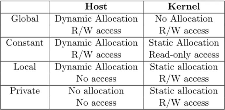
Work-items executing a kernel have access to four distinct memory regions [3]:
• Global Memory. This memory region permits read/write access to all work-items in all work-groups. Work-items can read from or write to any element of a memory object. Reads and writes to global memory may be cached depending on the capabilities of the device.
• Constant Memory: A region of global memory that remains constant during the execution of a kernel. The host allocates and initializes memory objects placed into constant memory.
• Local Memory: A memory region local to a work-group. This memory region can be used to allocate variables that are shared by all work-items within a work-group. It may be implemented as dedicated regions of memory on the OpenCL device.
Alternatively, the local memory region may be mapped onto sections of the global memory.
• Private Memory: A region of memory private to a work-item. Variables defined in one work-item’s private memory are not visible to another work-item.
Table 2.2 lists the OpenCL memory regions and their features.
Host Kernel
Global Dynamic Allocation No Allocation R/W access R/W access Constant Dynamic Allocation Static Allocation
R/W access Read-only access Local Dynamic Allocation Static allocation
No access R/W access Private No allocation Static allocation
No access R/W access
Table 2.2: OpenCL memory regions.
Hardware Model
The OpenCL platform consists of a host connected to one or more devices, also called OpenCL devices. Each device is composed of a set of Compute Units and each compute unit is further subdivided into a set of Processing Elements that are the fundamental units for computation (see Figure 2.15). An OpenCL application runs on the host and submits commands to a device for the execution of computations. The processing elements within a compute unit execute instructions in a SIMD or in a SPMD (Single-Program, Multiple-Data) fashion. In the first case the processing elements execute the same instruction at the same time while in the second case each processing element maintain its own program counter [3].
Communication Model
Host programs manage the execution of kernels through contexts and command queues. A context includes the following elements:
• Devices: The collection of OpenCL devices to be used by the host. • Kernels: The OpenCL functions that run on OpenCL devices.
Figure 2.15: The OpenCL hardware model.
• Memory Objects: A set of memory objects visible to the host and the OpenCL devices. Memory objects contain values that can be manipulated by instances of a kernel.
The elements listed above are manipulated by the host program using the OpenCL API. The host program puts commands into a command-queue that are flushed to the devices bound to a specific context. Commands can be of the following types:
• Kernel execution commands: Execute a kernel on the processing elements of a device.
• Memory commands: Transfer data to, from, or between memory objects, or map and unmap memory objects from the host address space.
• Synchronization commands: Constrain the order of execution of commands. For example the following function enqueues a command to execute a kernel on a device:
c l i n t clEnqueueNDRangeKernel ( cl command queue command queue , c l k e r n e l a K e r n e l , c l u i n t work dim , const s i z e t ∗ g l o b a l w o r k o f f s e t , const s i z e t ∗ g l o b a l w o r k s i z e , const s i z e t ∗ l o c a l w o r k s i z e , c l u i n t n u m e v e n t s i n w a i t l i s t , const c l e v e n t ∗ e v e n t w a i t l i s t , c l e v e n t ∗ e v e n t )
Commands in a queue can be executed in two ways:
• In-order Execution: Commands are launched in the order they appear in the command-queue and complete in order. In other words, a prior command in the queue completes before the beginning of the following command. This serializes the execution order of commands in a queue.
• Out-of-order Execution: Commands are issued in order, but do not wait to com-plete before following commands execute. Any order constraints are enforced by the programmer through explicit synchronization commands.
Synchronization can occur in two different scenarios: • Work-items in a single work-group.
• Commands enqueued to command-queue(s) in a single context.
In the first case synchronization is done using a barrier at which each work-item within a work-group must wait until all work-items of that group have reached the barrier. In the second case, commands in a command-queue can be synchronized using a command-queue barrier: every command preceding the barrier must be completed before the succeeding command can start its execution.


![Figure 3.1: Languages offer a subset of the CLR/CTS and a superset of the CLS (but not necessarily the same superset) [42].](https://thumb-eu.123doks.com/thumbv2/123dokorg/7374745.95832/49.892.330.602.159.444/figure-languages-offer-subset-clr-superset-necessarily-superset.webp)
![Figure 3.3: A Platform Invoke call to an un-managed DLL function [11].](https://thumb-eu.123doks.com/thumbv2/123dokorg/7374745.95832/57.892.233.706.158.330/figure-platform-invoke-managed-dll-function.webp)