UNIVERSITÀ DEGLI STUDI DI ROMA
"TOR VERGATA"
FACOLTÀ DI INGEGNERIA
DOTTORATO DI RICERCA IN INGEGNERIA DEI MATERIALI
CICLO XXI
Dielectric and EM properties of carbon filled epoxy resin
Paolo Travaglia
A.A. 2008/2009
Docente Guida/Tutor: Ing. Francesca Nanni
Index
Introduction ... 5
1 Conducting polymer composites... 7
1.1 Distribution of filler into the matrix and its consequence on electric properties ... 10
1.1.1 Influence of filler shape ... 11
1.1.2 Influence of resin, additives and manufacturing method ... 13
1.2 Main types of nanofillers ... 14
1.2.1 Carbon Black... 14
1.2.2 Carbon nanofibers ... 17
1.2.3 Carbon nanotubes... 20
1.3 Equivalent circuit analogy ... 23
1.4 References ... 23
2 Electromagnetic properties of materials: an overwiev... 29
2.1 Intrinsic EM parameters... 29
2.1.1 Microscopic approach to permittivity ... 32
2.1.2 Polarization caused by an alternating electrical field... 34
2.1.3 Absorbing mechanism in dielectric materials ... 36
2.2 Measuring equipment... 37
2.2.1 Vector network analyzer ... 37
2.3 Measuring techniques ... 38
2.3.1 Coaxial probe ... 38
2.3.2 Transmission line methods... 39
2.3.3 Free space... 40
2.4 Scattering parameters elaboration ... 40
2.5 References ... 42
3 Material and methods... 43
3.1.1 Acronym... 43
3.1.2 Resin... 43
3.1.3 Determination of filler content... 44
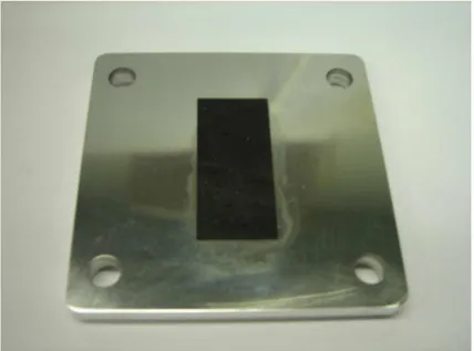
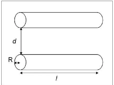
3.1.4 VNA measurement sample requirements and preparation ... 44
3.1.5 Dielectric percent variations calculations ... 45
4.1 Experimental ... 47
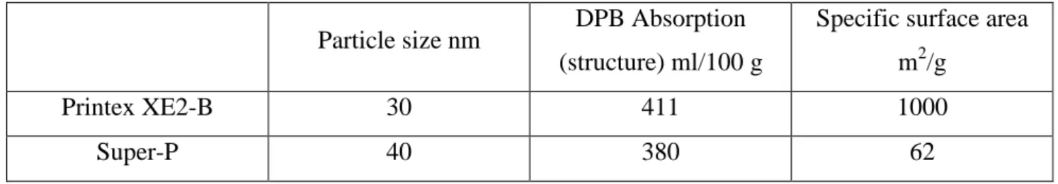
4.1.1 Degussa Printex XE2-B and Timcal Super-P ... 47
4.1.2 Fabrication procedure ... 47
4.1.3 Specimens characterization... 48
4.2 Results and discussion ... 48
4.2.1 Conducting paths morphologies... 48
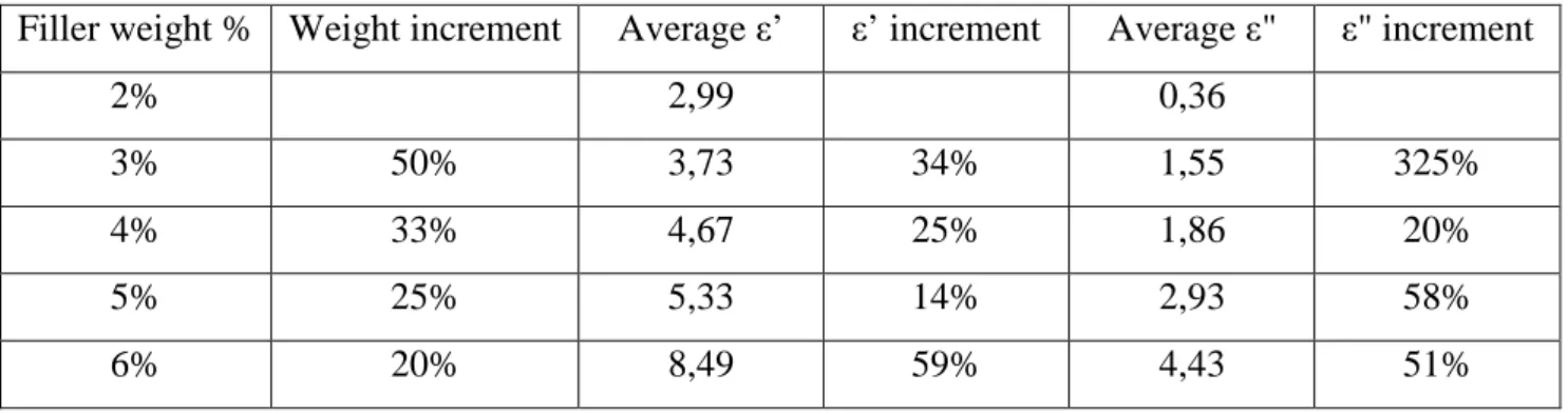
4.2.2 XE loaded samples... 49
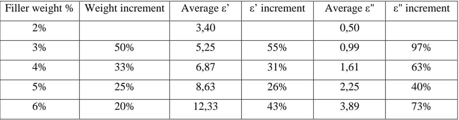
4.2.3 Super-P... 51
4.2.4 Electric interpretation of the conducting path morphologies and comparison on same filler basis ... 54
4.3 Conclusions... 57
4.4 References ... 58
5 Carbon nanofibers samples ... 59
5.1 Experimental ... 59
5.1.1 Pyrograf PR-19-XT-HHT ... 59
5.1.2 Sample production methods... 59
5.1.3 Characterization ... 61
5.2 Results and discussion ... 61
5.2.1 CNF Disagglomeration ... 61
5.2.2 Dispersion in resin and dielectric properties... 63
5.2.3 Review of the relationship between microstructure morphology and dielectric properties on the same filler % basis ... 72
5.3 Conclusions... 79
5.4 References ... 80
6 Carbon nanotubes samples... 81
6.1 Experimental ... 82
6.1.1 materials and fabrication procedure ... 82
6.1.2 Characterization ... 83
6.2 Results and discussion ... 83
6.2.1 Dispersion in solvent and in resin ... 83
6.2.2 Em measurements and Relationship between microstructure and dielectric properties: Type NT and SU samples ... 87
6.2.3 B6 Dielectric and EM properties ... 91
6.3 Conclusions... 94 6.4 References ... 94 7 CB CNF CNT comparison... 96 7.1 References ... 100 8 Conclusions... 101 Acknowledgment ... 103
Introduction
This thesis deals with the dielectric and absorbing properties at microwaves (x-band) of epoxy resin filled nanocomposites. Three different carbonaceous nanofillers were used in the experimental: carbon black (CB), carbon nanofibers (CNF) and carbon nanotubes (CNT). Moreover, various dispersion processes of nanofiller in the resin were tried, in order to analyze the effect of filler distribution on the dielectric properties of the resulting composites. Permittivity was measured using a vector network analyzer in x-band (8,2-12,4 GHz) using the waveguide method. Samples morphology was studied by FEG-SEM. Using the equivalent circuit analogy, a link between samples morphology and permittivity was attempted. The suitability of these materials as electromagnetic microwaves absorbers was finally assessed.
In carbon black samples, realized using fillers with different specific surface areas, the filler distribution within the resin is very different, producing small short branched clusters when using high surface areas filler, and long thick and meandering aggregates in the other case. In both samples the clusters are close to cylindrical shape and may be seen as parallel cylinders capacitors in the resin. As a consequence, high surface area samples present lower values of real permittivity (that takes into account capacity of the system), due to the smaller length of capacitor plates, but higher imaginary permittivity (linked to conductivity and dissipations effects) because, as noted above, the clusters are closely spaced, permitting the activation of hopping and tunnelling conduction modes. CB samples showed good performances as EM absorbers, reaching a peak of -38 dB using a sample 4 mm thick.
In samples loaded with high aspect ratio (CNF and CNT) the key parameter is their dispersion in the resin. In CNF experimentation, despite the use of different methodologies, an unsatisfying dispersion was achieved, with the resulting microstructure made of aggregates. The EM measurements highlighted that the higher the number and the smaller the dimension of the aggregates, the higher are ε’ and ε”,for the same reason found in the case of CB. With CNT, instead, very good dispersions were achieved, by means of the aid of surfactants and of a more powerful sonicator. The results demonstrate again that permittivity is linked to microstructure, with the same trend established with the other type of nanofillers. Nevertheless, in this case, a new evidence was found highlighting that there is an optimum level of dispersion, above which the CNT do not interact each other, resulting in very high ε’ and very low ε”, since dissipation through Joule effect is limited.
The absorbing performance of CNF and CNT demonstrate that too much filler, or too much dispersion of it (i.e. Low ε”), bring to a mostly reflective medium, with low absorbing performance.
An optimum formulation needs, therefore, to be found for every system as a compromise among material composition, microstructure and thickness.
Part of the experimental work (most of chapter 6 ) was carried out during the author secondment to Monash University (Clayton, Victoria Australia) under the supervision of Prof. George Simon.
1
Conducting polymer composites
Loading a non conductive polymer with conductive filler, either particles or fibres, produces different grades of conducting polymers composites (CPC). The benefit of coupling the ease of manufacturing, flexibility of shapes and application, low density and low cost with electric conductivity make them very attractive in several applications from antistatic coatings [1] to smart materials applications, to emi shielding and absorbing materials. CPC have found relevance in electronic devices manufacturing, where they are employed as conductive adhesive and circuit elements. Their usefulness has been boosted by the introduction of the Restriction of Hazardous Substances Directive (RoHS) in Europe, and similar laws in the USA, that ban the use of lead from electronic devices since the first of July 2006. Commonly, these adhesives consist on silver powder dispersed into a variety of polymers (DC electrical conductivity inside CPCs is caused by the formation of a network of conductive particles inside the matrix, as better explained in the following §1.1), like silicone polyurethane, polyamide and epoxy, depending on the adhesive required performance in terms of heat resistance, flexibility, mechanical resistance, etc. usually such materials possess low electrical resistivity and high thermal conductivity [2, 3].
CPC are also employed to produce regulators or sensors and also in electronic devices as fault current limiters in circuit protection [4, 5], exploiting their positive temperature coefficient of resistance. [6, 7]. When the CPC is heated above the design specification by the passage of a current, it swells resulting in the separation of conducting particles with a consequent increase of its electrical resistance. The regulator therefore shows two different electrical behaviours, as a function of the current: when the electrical current is close to the design parameter, the regulator shows low resistivity, when it increases above a certain level, the current flow is limited by the increase of the regulator resistivity. Commonly these devices are made of polyethylene matrix filled with carbon black. This kind of device can be found in pc or batteries against short circuit discharges.
In civil engineering self-diagnosis materials, showing both reinforcement and sensor performance in concrete structures, use the same principle. The sensor/reinforcement, in fact, shows an increase of electrical resistance as a consequence of increasing stress and/or strain. Under these conditions, in fact, in self-diagnosis components made of carbonaceous nanofiller in thermosetting resin, the increasing of matrix strain yields to carbon particles separation, resulting in enhanced macroscopic electrical resistance. this, in turn, can be direclty correlated to the level of stress bored by concrete structure . such behaviour was proven in self-monitoring composites tested both outside and inside concrete [8, 9].
Chemical sensors use the variation of resistivity caused by the swelling of the matrix after a certain time of exposure, when it adsorbs organic chemicals. A good sensor is the one that can give different electrical conductivity for different vapours [10-12].
Electromagnetic interferences (EMI) Shielding, electrostatic discharge (ESD) protection and microwave absorbing materials (MAM) are the major applications for conductive polymer composites. The first and latter of them are involved in electronic devices and environments protection and antenna decoupling. Shielding usually performs by reflecting the incident waves, sending them back in the medium from which they came from. To reflect the incident radiation, the shield must have mobile charge carriers (electron or holes) which interact with the electromagnetic fields in the radiation. Materials employed as shields need therefore to be somehow electrically conducting, even if a volume resistivity of 1 Ωcm is typically sufficient. EMI shields can therefore be made of either conductive materials, i.e. metals, or CPC, that can be employed even below percolation . EMI shielding is mostly employed to house electronic equipment, either to provide an electronic-noise-free environment, or shield other electronic components or workers from the noise and radiations generated [13-17].
ESD requirements are less stringent, and they required lower surface resistivity. ESD is employed where there is a constant built up of static electricity, and thus a need to disperse it, as in airplane fuselages [1] and tires, conveyor belts and weaving machines, wherever a relative motion between dissimilar materials occurs [18, 19].
Fig. 1-1 illustrates the typical ranges of surface resistivity of CPC and of their most common applications.
Fig. 1-1 Surface resistivity of conducting polymer composites and their most common applications. (Available f rom: http://www.rtpcompany.com/products/ conductive/index.htm.)
Microwave absorbing materials, finally, provide a more efficient electromagnetic wave protection, since they do not reflect incident waves, but dissipate them through the material with virtually no scattering.
Fig. 1-2 On the left shielding, on the right absorbing
The mechanism of absorption is much more complex because it involves both the instrinic porperties of the component as well as its extrinsic characteristics, as geometrical shape and dimensions. from the material point of view, the dissipation of the energy associated to the incident waves requires the presence of electric or magentic dipoles able to interact with the electromagnetic fields. These dipoles are responsible for different polarization mechanisms, which occur in the material at difference frequencies (cfr. §2.1.1). CPC are ideal candidate materials to realize absorbing structures, thank to their versatility and possibility to insert dipoles by adding pure conductive, dielectric or magnetic fillers within the insulating matrix [20, 21]. barium titanate, for instance, was used as filler in polyurethane and polyaniline as matrix to produce 2,5 mm thick em
absorbing composites in [22]. peaks of 25 dB absorption at 11,2 GHz were obtained. More than 40 db of attenuation at 8 GHz were obtained by[20] using abs as matrix and 30% vol of barium titanate. In [23] it is reported that 8% vol of in epoxy in samples 6 mm thick yields 20 dB attenuation at 13 GHz. Hexaferrites were proposed as magnetic fillers: Co2Y-type hexaferrite
(Ba2CuxCo2-xFe12O22, x=0,1) were employed as filler of rubber matrix leading to 35 dB attenuation
in 3 mm thick samples[24]. the contemporarily use of a conductive and magnetic filler was proposed to [25]: a mix of magnetite, Co-Ti substituted hexaferrite and graphite gives a peak of 22 db attenuation with 2 mm thick samples,.
1.1
Distribution
of
filler
into
the
matrix
and
its
consequence on electric properties
A very important parameter when dealing with EM properties of CPC is the distribution of filler or nanofiller within the matrix. Historically this feature has been investigated in the theory of percolation, i.e. the formation of a continuous network of conductive filler leading to dc conductivity.
Dishovsky and Grigorova in [26] noted that CB concentration influences the EM properties of a filled polymer and that the best values of absorption are obtained just before the onset of percolation. One of the ways to explain the electrical properties of conductive particles filled polymers is percolation theory. Percolation started as a lattice model to study the statistical probability of fluid flowing through a static medium, it was then used to model the conductive behaviour against filler concentration [27]. Percolative behaviour can be recognised when, while increasing the filler content, there is a sharp decrease, in composite resistivity, (several orders of magnitude). The percolation threshold is then identified by the filler volume percent at the resistivity abrupt decrease. The abrupt change in electrical properties is caused by the formation of the so called “infinite cluster”, a network-like conductive pattern inside the composite that encompass the whole volume (Fig. 1-3).
Fig. 1-3 Percolation threshold and formation of infinitive cluster [19]
Increasing the filler content above the percolation threshold produces just a slight variation in composite resistivity. If resistivity keeps decreasing after the percolation threshold in a significant way, it means that the three-dimensional conductive-network has not formed yet and conductivity is prevalently caused by tunnelling between close, but not in contact, filler particles. Tunnelling happens when particles are approximately 10 nm or closer [18, 28]. The relationship between current and voltage gives an indication of the type of mechanism active inside the composite [29, 30]. If conductive filler inside the matrix touch each other the relationship will be Ohmic linear, instead when tunnelling is the prevalent mechanism, the relationship between current and voltage is best matched by a power law [30, 31].
Ways to lower the filler content need to be studied when designing EMI shielding materials since the best use of the filler means higher dielectric properties at constant filler ratio (cfr. §1.1.2) or less filler to achieve the desired values of permittivity.
Percolation threshold, electrical and most important for EM application dielectric properties below the percolation threshold, depends on numerous factors including filler aspect ratio [32], conductivity, morphology [28], dispersion and distribution, affinity with the matrix [33], polymer matrix cristallinity [34] and surface tension, manufacturing, and eventual additives [34-37]. In the following some of these parameters will be shortly discussed.
1.1.1 Influence of filler shape
(
)
t c v v ρ ρ = 0 − − (eq. 1.1)Where ρ is the composite electrical resistivity (Ω cm)
ρ
0 is a scaling factor (Ω cm, the scalingfactor is needed since percolation theory is valid only assuming the matrix has zero conductance or the filler zero resistance), v is the filler volume fraction and v is volume fraction at percolation. c
The critical exponent t is related to the lattice dimension (i.e. if a 2D or 3D lattice developed/was studied), and varies between 1,65 and 2 for three-dimensional lattices [27, 38]. If the filler used is fibrous instead of spherical (i.e. CNF, CNT) the exponent is higher than 2 and in particular as reported in [39], close to 3. According to percolation theory, using spherical filling factors, a random packing in three dimensions, yields v around 16% volume fraction [28], fibrous fillers or c
high structure CB1 show v of only several percent or even less than one percent. Fig. 1-4 show the c
filler aspect ratio needed to achieve percolation by a certain volume fraction
Fig. 1-4 percolation volume fraction vs filler aspect ratio [40]
Percolation, as stated and shown in Fig. 1-4, can be drastically reduced using fillers with an aspect ratio >1. Fig. 1-5 shows graphically the consequences: 10% surface fraction of filler is randomly dispersed on a same surface plane, the effect of aspect ratio is substantial, while 10% volume is NOT enough to provide a percolating network of spherical particles, it is more than enough when a
fibrous filler is used. On a same filler basis, in fact, the high aspect ratio filler provides more occasions of contact among particles compared to the case of close to round fillers (aspect ratio close to 1).
Fig. 1-5 10% surface of filler fraction , spherical particles (left) fibrous filler (right)
1.1.2 Influence of resin, additives and manufacturing method
Before dealing with the influence of manufacturing methods on the shape and performance of the conductive paths, it is useful to devote some words to the effect of resin on the resulting properties, of the CPC. Kato and Miyashita [34] determined that polymer cristallinity has a very high influence. CB is present only in the amorphous regions, thus increasing the local filler content easing the formation of a percolative network. On the same paper a remark about the influence of polar resins states that polar matrixes have better wetting properties and so give more conductive composites for the same filler weight. Cheah et al. [33] agrees with the previous mentioned paper about polar polymers, but they state that what matters, instead of taking just the absolute value of matrix polarity, is matrix-filler difference in polarity. Cheah also shows that to achieve good percolation values a good dispersion (the particles are not grouped together in big bundles) is needed but not a good distribution (the particles are evenly distributed inside the matrix). Moreover, quite surprising, it was found that an optimal distribution of filler inside the matrix may lead to worse electric properties. Grunlan et al. [37] tried the use of an additive to promote filer dispersion, but they found that the presence of smaller aggregates provide lower electrical conductivity at a higher percolation threshold. Schueler et al in [35] went further adding CuCl2 to lower the energy
barrier that prevents the formation of bigger agglomerates that, from their point of view, help conductivity. Schueler also documented that high shear forces are enough to disperse CB inside a matrix and reach conductivity. In a later paper [41] even CNT were dispersed using just an energetic stirring. Instead of additives that help dispersion Yoon and co-workers [36] used additives that help conduction, via increasing hopping phenomena, γ-aminopropyltrimethoxysilane (APS)
and trimethoxy-npropylsilane (TPS) were tried. The former was proved to lower significantly the percolation limit.
Another important aspect related to the nature of filler, which arises when dealing with fibrous fillers is their very strong agglomeration. Before insertion in the resin it is therefore necessary to disagglomerate the fibres. Many different methodologies were tried, among which there is the sonication method, which was chosen by the author for in this experimental work. Dispersion can be carried out via sonication directly in resin or previously in solvent. Song [42] produced two series of CNT/epoxy samples; in the former CNT were sonicated in resin, while in the latter a solvent was used to sonicate CNT and the resin was added later. The results from mechanical tests were controversial, while electrical conductivity showed important improvements by achieving good filler dispersion with solvent use. The nature of solvent, though, is important since it has an influence on the resulting properties of the composite, as in the case of functional groups formed in the cured epoxy [43]. Sonication can lead to the possibility of fibres cutting if not carefully performed in terms of time and power of sonication; to limit this bad evenience it was suggested that nanofibres doping may provide a better way to preserve the aspect ratio and integrity of fillers [44]. It is also important to remember that, when dealing with almost mono-dimensional fillers as in the case of CNF and CNT, there may be an orientation effect if the composite is extruded before curing.
This very short overview evidences how many aspects and parameters must be taking in count when preparing nanofilled composites for electromagnetic applications. In the following paragraphs the main characteristic of any nanofiller used in this thesis, i.e. CB, CNF and CNT, will be briefly discussed.
1.2
Main types of nanofillers
1.2.1 Carbon Black
Carbon black (CB) is widely used as a filler in several industrial process, such as a reinforcing filler, to improve dimensional stability, conductive filler, ultraviolet light stabilizer, antioxidant to prolong the lifetime of rubber, and pigment or colorant. CB is an amorphous form of carbon with a structure similar to disordered graphite: “When aromatic hydrocarbons are subjected to incomplete combustion at high temperature their molecules will dissociate through the rupture of C-H bonds. Subsequently, carbon atoms and aromatic radicals react to form layer structures composed of hexagonal carbon rings, which tend to stack in three to four layers, forming crystallographic structures” [45]. CB has a turbostratic structure, where the graphite layers are rotated or shifted
Fig. 1-6 CB graph planes [47]
CB essentially consist of elemental carbon in the form of near spherical particle of colloidal size coalesced into particle aggregates and agglomerates. A CB particle is a small spheroidal non-discrete component of a CB aggregate, particle diameters can range from less than 20 nm in some furnace grades to few hundred nm in thermal blacks. Several CB particles form a CB aggregate, a discrete, rigid, colloidal entity of coalesced particles, it is the smallest dispersible unit of carbon black, aggregates dimensions can range from as small as 100 nm to a few micrometers Fig. 1-7.
Fig. 1-7 Schematic showing the distinction between carbon black particles and aggregate.
Among several characteristics of CB, two influence the microstructure of the resulting CPC most: structure and specific surface area. Structure describe the complexity of the shape of the CB aggregates, they vary quite widely in morphology, from the large individual spheres found in some thermal black to small highly complicated, branched aggregates in high structure{Balberg,
2002 #35}, high surface area CB [48]. The complex and varied shapes of the CB aggregates lead to the creation of voids between the aggregates in any sample of CB that are greater than the voids that would be created if the aggregates were simple spheres of equivalent size. It is this fact that has lead to the commonly used techniques of measuring internal void volumes as a means of indirectly assessing the shape, or “structure” or aggregates within a carbon black sample. In general the greater the measured internal void volume, the more complex, open, and branched the aggregates
volumetric measurement under specific pressures or, more commonly, oil absorption measurements. In either case it is clear that this is a parameter of CB that has a significant influence on the compound in which the CB is dispersed. Increasing only the structure of CB used in a rubber compound will typically increase the compound’s hardness, viscosity, stress at high strain and wear resistance. The specific surface area is by definition the available surface area in square meters per unit mass of CB in grams, it also is a measure of porosity.
Fig. 1-8 TEM micrography of low structure (N326) and high structure (N358) CB
It is several years CB is used in EM application. A 35 dB shielding efficiency was reported in 1996 [49] with a polypropylene sample loaded with 40%w CB at 10 GHz (sample thickness not reported). Another paper from 2000 [50] reports a SE of 20 dB in X-band as its best result when CB and ethylene-vinyl acetate were used, sample thickness was 3,5 mm. Absorbing materials were mostly studied to be used in military applications and as a consequence most of the research was classified, it is now finding their way into mainstream applications on mobile phones and other wireless gadgets. CB was the first filler used in such applications, such as [51, 52] that report respectively a 25 dB peak at 10,5 GHz with samples loaded with 10% CB and –30 dB at various frequencies depending on the thickness. Barba [52] also provides a graphical way to understand how absorbing properties of a composite are not just influenced by filler loading but also from frequency and thickness Fig. 1-9.
Fig. 1-9 Influence of frequency and thickness on the absorbing properties of two different CB filled polymers [52]
Wen et al. [53] used paraffin as a binder to test the absorbing properties of CB and catalysed CB and they achieved more than 20 dB attenuation at 16 GHz with a thickness of 6 mm.
A paper that deals with RAS is [54] by Chin and Lee, they manufactured a single layer absorber that 2,93 mm thickness and loaded with 0,02%w of CB it achieves 55dB attenuation at 10,1 GHz.,
1.2.2 Carbon nanofibers
Carbon nanofibers (CNF) and carbon nanotubes (CNT), are high aspect ratio conductive carbon nanofilles. It is possible to think of them as one-dimensional fillers, due to their high aspect ratio. CNF are much cheaper than CNT, have comparable electrical properties, less microstructural defects and lower density, they also are somewhat easier to disentangle but their diameter is bigger (CNF diameter ranges from tents to hundreds of nm) and often have lower aspect ratio [19, 55], which sometimes make them performance less efficient that those of CNT.
1.2.2.1 CNF structure and properties
As produced CNF have varying dimension, structure, mechanical, thermal and, most important for conductive polymers, electrical properties [56] Before post treatment CNFs are covered by a layer of amorphous carbon that render them less conductive: “Because the filaments tend to clog the rear of the reactor tube, eventually spending many seconds within the decomposing methane atmosphere, a layer of vapour-deposited carbon both thickens the individual fibres and cements them together in large clumps. The exterior layer of vapour-deposited carbon is not as graphitic as
the interior cylinder, and has graphene planes which are primarily longitudinally oriented” [57] (Fig. 1-10).
CNF structure common features are a hollow core and graphite planes rolled parallel or at an angle around their axis [58, 59] (Fig. 1-10), the stacked planes are nested within each other. CNF are produced with different structures including bamboo-like, parallel and cup-stacked, the d-spacing of the graphene sheets was reported as 0.34 nm (the same as that in MWNTs and graphite platelets) [58, 60]. Single and double layer CNF morphology were identified by Uchida and al. [59], Fig. 1-11 shows a double layer one where, a truncated cone inner layer structure is enveloped by an outer layer of planes of graphite parallel to the axis.
Fig. 1-11 TEM image of a double layer CNF [58].
Fig. 1-12 shows a high resolution transmission electron microscopy (HRTEM) image of a side-wall of a CNF (the inset is a schematic illustrating the structure of cup-stacked VGCNF). The nanofiber is clearly seen to have a hollow core surrounded by concentric cup-stacked planes.
Staked cups structure has a large number of reactive edges both inside and outside the nanofiber [61]. The way graphite sheets (about 3-5) fold at the end of the stacked cones structure is depicted in Fig. 1-13. Fig. 1-13a shows the structure of single layer CNF while Fig. 1-13b depicts a double layer one, HRTEM inset shows the graphite folds [19].
Fig. 1-13 HRTEM and schematics of graphene loops that folds at the end of the angled graphene planes [19].
Recently CNF have been proposed for EM applications. Yang et al. [62] found a shielding effectiveness (SE) of 26 dB at 200 MHz with a 1,45 mm sample LCP loaded with 15%w of filler. Zhang [63] studied SE of polyesterpolyol loaded with CNF in K, Q, V bands, and obtained 35 dB at 26 GHz and 60 dB at 75 GHz hinting at absorption contribution since increasing the thickness of the samples produced an increase in shielding. Lee [64] tried 40%w CNF filled PVA of just 30 µm thickness and compared it with a composite filled with the same quantity of CB: It was found that before thermal treating the CNF composite behaved worse than CB filled PVA, while after thermal treatment the SE of CNF was better than CB. Yang et al. [65] compared SE of CNF and MWCNT filled polymer in X band and found that SE of MWCNT was considerable higher than of CNF samples being the se of 5%w loaded samples at 10 GHz, of respectively 7,5 and 24 dB for CNF and CNT specimens. In a subsequent paper the same authors reached 21,9 dB SE in Ku-band, with a filler content in polystyrene of respectively 10%w CNF and 3%w CNT.
1.2.3 Carbon nanotubes
In the very last years, CNT had been a subject on the forefront of scientific research, with many researchers scrambling to find ways to get the most from their properties (electric, thermal and mechanic) that were predicted to be very high. as reported in [66], “CNT can be visualized as a
structure formed with each carbon atom having four nearest neighbours arranged in a tetrahedron, graphite is formed as a 2-D sheet of carbon atoms arranged in a hexagonal array. In this case, each carbon atom has three nearest neighbours. ‘Rolling’ sheets of graphite into cylinders forms CNT. The properties of CNT depend on atomic arrangement (how the sheets of graphite are ‘rolled’), the diameter and length of the tubes, and the morphology, or nanostructure. Nanotubes exist as either single-walled or multi-walled structures, and multi-walled carbon nanotubes (MWCNT) are simply composed of concentric single-walled carbon nanotubes (SWCNT)” (Fig. 1-14)
Fig. 1-14 Sketch of a single wall nanotube
Multi-walled CNT are composed of a number of concentric single walled CNT held together with relatively weak van der Walls forces. The multi-layered structure of these CNT further complicates the modelling of their properties.
The low density of CNT (between 1,3 and 1,75 g/cm2 [67]) high aspect ratio and extraordinary mechanical properties (tensile strength 50-500 GPa and modulus of 1500 GPa when SWCNT are considered, and 10-60 and 1000 GPa when testing MWCNT [68]) make them particularly attractive for reinforcement in composite materials. In general, the tensile modulus and strength of polymer-rich CNT composites are found to increase with CNT loading, dispersion, and alignment in the matrix. However, the results at low CNT concentrations typically remain far behind the idealized theoretical predictions The gap between the predictions and experimental results arises from imperfect dispersion and poor load transfer. When the interfacial adhesion between the phases is weak, the CNT behave as holes or nanostructured flaws. Moreover, even modest CNT agglomeration impacts the diameter and length distributions of the filler and overall is likely to decrease the aspect ratio (a parameter in the models). In addition, CNT agglomeration reduces the modulus of the filler (another parameter in the models) relative to that of isolated CNT because there are only weak dispersive forces between CNT.
The potential of CNT as conducting fillers in multifunctional polymer composites has been successfully realized. Several orders of magnitude enhancement in electrical conductivity, σ, has been achieved [69] with a very small loading, below 0.1 %w of nanotubes in the polymer matrices,
etc. A variety of applications are being pursued using these conductive composites: electrostatic dissipation [70], electrostatic painting [71], electromagnetic interference (EMI) shielding [72], and transparent conductive coating [73] The percolation threshold for the electrical conductivity in CNT/polymer composites is influenced by several CNT characteristics most important among them aspect ratio, surface area and dispersion [42, 74], some authors suggest that shorter CNT and some agglomeration permits a lower percolation threshold [41].
As noted above for CNF, disagglomeration and dispersion of CNT inside the matrix is a key issue in any field of application [60]. Different methods of manufacturing can be used to produce filled polymers and disperse CNT such as the ones described in [19, 43, 68, 75]. Permittivity in X-band highlights the effect of CNT type, manufacturing and filler dispersion on the dielectric properties of the resulting composite. For instance Wu et al. [76] reports a relative real permittivity of less than 6 when an epoxy sample is loaded with 4,7%w, while Huang and co-workers [72] report a value of 25 with a loading of 5%w of SWCNT.
CNT have been used in shielding and absorbing applications, obtaining good results. 25 dB attenuation using epoxy filled with 15%w of long SWCNT at a thickness of 2 mm [72] and 16 dB when a polyurethane film loaded with 20%w is considered [77]. Umishita et al. [78] has measured the absorbing and shielding properties of MWCNT, their results are of about 20 dB attenuation for 0,22%w at 5,8GHz, increasing the filler content they obtained 45 dB shielding with PEEK as a matrix and a thickness of 4 mm. Absorbing application are less frequently published since their interest lays mostly in military application and as such most of the results are classified, but what is published is very promising such as more than 30 dB attenuation of CNT dispersed in silicon oil at a concentration of 0,25%w [79]. A peak attenuation of 22 dB at 11,4 GHz using a sample 1 mm thick is reported in [80] , but they Do not report how much filler was used. An absorption peak of 12 dB of attenuation on a sample 1,80 mm thick at 14 GHz is reported in [81] using polyester as matrix, but even in this case, the amount of filler used is not revealed. Multilayer absorbers and radar absorber structures (RAS) in form of composite sandwiches were also produced. RAS originate from the idea to reach valuable absorbing performance by exploiting wave interference. Such structures derive from specific electromagnetic design, that usually define a stacking sequence of layers, each one of which preset peculiar dielectric and/or magnetic properties and thickness. In [82] epoxy-glass fibres face sheets were loaded with CB and the polyurethane core was loaded with CNT, with the result that an attenuation of about 30 db were achieved. another example of RAS is the topic of [83], where a genetic algorithm is used to optimize the layers of MWCNT filled epoxy/glass fibres with a remarkable broadband absorption of more than 10 db over the whole
X-absorbers RAS sandwich produced, in this case epoxy-glass fibres face sheets loaded with CB and the polyurethane core loaded with CNT, got an attenuation of around 30 dB [82].
1.3
Equivalent circuit analogy
As outlined in §1.1 most of the research involving CPC was focused on lowering the percolation threshold, and scant attention was given till recently to other EM properties that are equally, if not more, affected by the morphology of filler networks inside the matrix. Nakamura [84] had shown that if a CPC is interpreted as an electrical equivalent circuit an increase in filler content increases its capacity and decrease its resistivity. In a successive paper [85] he suggested that dead branches of CB aggregates in the resin may act as capacitors and may be the cause of dielectric relaxation at high frequency. Further along these lines, Farfán et al. [86] showed that CPC with various filler content below percolation show frequency dependent resistance, which is a typical capacitor behaviour. In its 2006 paper Saib et al.[32] found that conductivity is frequency dependent and there is a high capacitive coupling between filler particles. In this work three different filler types were tested, some of them were also used in different ways, producing a range of different network morphology. Dielectric results were then linked with the morphology as obtained by SEM analysis using an equivalent circuit analogy. The circuit analogy as outlined above interpret the CPC as a circuit composed of capacitors and resistances,
ε
r′ represent the ability of the material of store energy, it is then a measurement of the increase of equivalent capacitors inside the sample. These capacitors are produced by dead branches as suggested by Nakamura, but also by close spaced filler, in fact the value of capacitance is proportional to the surface of the conducting filler and inversely proportional to the distance among them. It is then safe to assume that the capacitance of the system increases when the surface area of the particles increases and when filler is better dispersed, since it creates new interface surfaces and so new capacitors, those capacitors will also have close spaced plates contributing even more to the increase in capacitance. The decrease in resistivity as the filler increases is indicated byε
r′′ and is influenced by the formation of morecontacts between filler particles allowing a rapid dispersion of the charge by Joule effect. The author hopes to have provided compelling proof in the following chapter to prove that the equivalent circuit analogy is a useful way to link the sample microstructure with the dielectric properties.
1.4
References
[1] Kupke M, Wentzel HP, Schulte K. Electrically conductive glass fibre reinforced epoxy resin. Materials Research Innovations. 1998;2(3):164-9.
[2] Kraass KH. Electrically conducting rubber-a new material for electronics. Telecommunications and Radio Engineering, Part 2 (Radio Engineering). 1976;31(3):117.
[3] Ouyang J, Yang Y. Conducting polymer as transparent electric glue. Advanced Materials. 2006;18(16):2141-4.
[4] Duggal AR. An upper limit for high power switching with a polymer current limiter device. IEEE Transactions on Components and Packaging Technologies. 2000;23(3):490-6.
[5] Owen F. Protect your circuits. Sensors. 2001;18(3):62-3.
[6] Horibe H, Kamimura T, Yoshida K. Electrical conductivity of polymer composites filled with metal. Japanese Journal of Applied Physics, Part 1 (Regular Papers, Short Notes & Review Papers). 2005;44(6A):4171-5.
[7] Horibe H, Kamimura T, Yoshida K. Electrical conductivity of polymer composites filled with carbon black. Japanese Journal of Applied Physics, Part 1 (Regular Papers, Short Notes & Review Papers). 2005;44(4A):2025-9.
[8] Nanni F, Auricchio F, Sarchi F, Forte G, Gusmano G. Self-sensing CF-GFRP rods as mechanical reinforcement and sensors of concrete beams. Smart Materials and Structures. 2006;15(1):182-6.
[9] Nanni F, Ruscito G, Forte G, Gusmano G. Design, manufacture and testing of self-sensing carbon fibre-glass fibre reinforced polymer rods. Smart Materials and Structures. 2007;16(6):2368-74.
[10] Bin Z, Xianming D, Wei S, Dingcai W, Ruowen F, Bin Z, et al. Electrical response and adsorption performance of novel composites from polystyrene filled with carbon aerogel in organic vapors. Sensors & Actuators: B Chemical. 2008;132(1):60-6.
[11] Dong XM, Fu RW, Zhang MQ, Zhang B, Rong MZ. Electrical resistance response of carbon black filled amorphous polymer composite sensors to organic vapors at low vapor concentrations. Carbon. 2004;42(12-13):2551-9.
[12] Arshak K, Adley C, Moore E, Cunniffe C, Campion M, Harris J. Characterisation of polymer nanocomposite sensors for quantification of bacterial cultures. Sensors & Actuators: B Chemical. 2007;126(1):226-31.
[13] Yi H, Ning L, Yanfeng M, Feng D, Feifei L, Xiaobo H, et al. The influence of single-walled carbon nanotube structure on the electromagnetic interference shielding efficiency of its epoxy composites. Carbon. 2007;45(8):1614-21.
[14] Awerkamp DR. Shielding effectiveness of filled composites and coated plastics. 1981; New York, NY, USA: IEEE; 1981. p. 277-80.
[15] Heiser JA, King JA, Konell JP, Sutter LL. Shielding effectiveness of carbon-filled nylon 6,6. Polymer Composites. 2004;25(4):407-16.
[16] Simon RM. EMI shielding with aluminium flake filled polymer composites. 1984; New York, NY, USA: IEEE; 1984. p. 732-5.
[17] Yang Y, Gupta MC, Dudley KL. Studies on electromagnetic interference shielding characteristics of metal nanoparticle- and carbon nanostructure-filled polymer composites in the Ku-band frequency. Micro & Nano Letters. 2007;2(4):85-9.
[18] Strumpler R, Glatz-Reichenbach J. Conducting polymer composites. Journal of Electroceramics. 1999;3(4):329-46.
[19] Al-Saleh MH, Sundararaj U. A review of vapor grown carbon nanofiber/polymer conductive composites. Carbon. 2009;47(1):2-22.
[20] Moulart A, Marrett C, Colton J. Polymeric composites for use in electronic and microwave devices. Polymer Engineering and Science. 2004;44(3):588-97.
[21] Folgueras LDC, Alves MA, Rezende MC. Development, characterization and optimization of dielectric radar absorbent materials as flexible sheets for use at X-band. 2007; Piscataway, NJ 08855-1331, United States: Institute of Electrical and Electronics Engineers Inc.; 2007. p. 488-91.
[22] Abbas SM, Chandra M, Verma A, Chatterjee R, Goel TC. Complex permittivity and microwave absorption properties of a composite dielectric absorber. Composites Part A: Applied Science and Manufacturing. 2006;37(11):2148-54.
[23] Chen X, Wang G, Duan Y, Liu S. Electromagnetic characteristics of barium titanate/epoxide resin composites in X and Ku bands. Journal of Alloys and Compounds. 2008;453(1-2):433-6. [24] Li X, Gong R, Feng Z, Yan J, Shen X, He H. Effect of particle size and concentration on microwave-absorbing properties of CuxCo2-xY (x=0, 1) hexaferrite composites. Journal of the American Ceramic Society. 2006;89(4):1450-2.
[25] Dishovski N, Petkov A, Nedkov I, Razkazov I. Hexaferrite contribution to microwave absorbers characteristics. Magnetics, IEEE Transactions on. 1994;30(2):969-71.
[26] Dishovsky N, Grigorova M. On the correlation between electromagnetic waves absorption and electrical conductivity of carbon black filled polyethylenes. Materials Research Bulletin. 2000;35(3):403-9.
[27] Kirkpatrick S. Percolation and Conduction. Reviews of Modern Physics. 1973;45(4):574. [28] Balberg I. A comprehensive picture of the electrical phenomena in carbon black-polymer composites. Carbon. 2002;40(2):139-43.
[29] Yui H, Wu G, Sano H, Sumita M, Kino K. Morphology and electrical conductivity of injection-molded polypropylene/carbon black composites with addition of high-density polyethylene. Polymer. 2006;47(10):3599-608.
[30] Bar H, Narkis M, Boiteux G. The electrical behavior of thermosetting polymer composites containing metal plated ceramic filler. Polymer Composites. 2005;26(1):12-9.
[31] Chekanov Y, Ohnogi R, Asai S, Sumita M. Electrical properties of epoxy resin filled with carbon fibers. Journal of Materials Science. 1999;34(22):5589-92.
[32] Saib A, Bednarz L, Daussin R, Bailly C, Lou X, Thomassin J-M, et al. Carbon nanotube composites for broadband microwave absorbing materials. IEEE Transactions on Microwave Theory and Techniques. 2006;54(6):2745-53.
[33] Cheah K, Simon GP, Forsyth M. Effects of polymer matrix and processing on the conductivity of polymer blends. Polymer International. 2001;50(1):27-36.
[34] Kato H, Miyashita Y. Qualification of the electrical conducitivity of carbon black filled polymeric materials. 1990; Pocono Manor, PA, USA: Publ by IEEE, Piscataway, NJ, USA; 1990. p. 417-24.
[35] Schueler R, Petermann J, Schulte K, Wentzel H-P. Agglomeration and electrical percolation behavior of carbon black dispersed in epoxy resin. Journal of Applied Polymer Science. 1997;63(13):1741-6.
[36] Yoon HG, Kwon KW, Nagata K, Takahashi K. Changing the percolation threshold of a carbon black/polymer composite by a coupling treatment of the black. Carbon. 2004;42(8-9):1877-9.
[37] Grunlan JC, Bloom FL, Gerberich WW, Francis LF. Effect of dispersing aid on electrical and mechanical behavior of carbon black-filled latex. Journal of Materials Science Letters. 2001;20(16):1523-6.
[38] Weber M, Kamal MR. Estimation of the volume resistivity of electrically conductive composites. Polymer Composites. 1997;18(6):711-25.
[39] Bryning MB, Islam MF, Kikkawa JM, Yodh AG. Very low conductivity threshold in bulk isotropic single-walled carbon nanotube-epoxy composites. Advanced Materials. 2005;17(9):1186-91.
[40] Bigg DM. EFFECT OF COMPOUNDING ON THE CONDUCTIVE PROPERTIES OF EMI SHIELDING COMPOUNDS. Advances in Polymer Technology. 1984;4(3-4):255-66.
[41] Martin CA, Sandler JKW, Shaffer MSP, Schwarz MK, Bauhofer W, Schulte K, et al. Formation of percolating networks in multi-wall carbon-nanotube-epoxy composites. Composites Science and Technology. 2004;64(15):2309-16.
[42] Song YS, Youn JR. Influence of dispersion states of carbon nanotubes on physical properties of epoxy nanocomposites. Carbon. 2005;43(7):1378-85.
[43] Lau K-T, Lu M, Lam C-K, Cheung H-Y, Sheng F-L, Li H-L. Thermal and mechanical properties of single-walled carbon nanotube bundle-reinforced epoxy nanocomposites: The role of solvent for nanotube dispersion. Composites Science and Technology. 2005;65(5 SPEC ISS):719-25.
[44] Chun K-Y, Choi SK, Kang HJ, Park CY, Lee CJ. Highly dispersed multi-walled carbon nanotubes in ethanol using potassium doping. Carbon. 2006;44(8):1491-5.
[45] Huang J-C. Carbon black filled conducting polymers and polymer blends. Advances in Polymer Technology. 2002;21(4):299-313.
[46] Donnet J-B, Bansal RC, Wang M-J. Carbon black : science and technology. 2nd ed. New York: Dekker 1993.
[47] Donnet J-B. Fifty years of research and progress on carbon black. Carbon. 1994;32(7):1305-10.
[48] Brosseau C, Boulic F, Queffelec P, Bourbigot C, Le Mest Y, Loaeca J, et al. Dielectric and microstructure properties of polymer carbon black composites. Journal of Applied Physics. 1997;81(2):882-91.
[49] Kaynak A, Polat A, Yilmazer U. Some microwave and mechanical properties of carbon fiber-polypropylene and carbon black-polypropylene composites. Materials Research Bulletin. 1996;31(10):1195-206.
[50] Das NC, Khastgir D, Chaki TK, Chakraborty A. Electromagnetic interference shielding effectiveness of carbon black and carbon fibre filled EVA and NR based composites. Composites Part A: Applied Science and Manufacturing. 2000;31(10):1069-81.
[51] Kwon SK, Ahn JM, Kim GH, Chun CH, Hwang JS, Lee JH. Microwave absorbing properties of carbon black/silicone rubber blend. Polymer Engineering and Science. 2002;42(11):2165-71.
[52] Barba AA, Lamberti G, D'Amore M, Acierno D. Carbon black/silicone rubber blends as absorbing materials to reduce Electro Magnetic Interferences (EMI). Polymer Bulletin. 2006;57(4):587-93.
[53] Wen B, Jijun Z, Yuping D, Xingguo Z, Yanbo Z, Chuang D, et al. Electromagnetic wave absorption properties of carbon powder from catalysed carbon black in X and ku bands. Journal of Physics D (Applied Physics). 2006;39(9):1960-2.
[54] Chin WS, Lee DG. Development of the composite RAS (radar absorbing structure) for the X-band frequency range. Composite Structures. 2007;77(4):457-65.
[55] Cooper CA, Ravich D, Lips D, Wagner HD, Mayer JJ. Distribution and alignment of carbon nanotubes and nanofibrils in a polymer matrix. Composites Science and Technology. 2002;62(7-8):1105-12.
[56] Van Hattum FWJ, Serp P, Figueiredo JL, Bernardo CA. Effect of morphology on the properties of vapour-grown carbon fibres. Carbon. 1997;35(6):860-3.
[57] Tibbetts GG, Lake ML, Strong KL, Rice BP. A review of the fabrication and properties of vapor-grown carbon nanofiber/polymer composites. Composites Science and Technology. 2007;67(7-8):1709-18.
[58] Miyagawa H, Rich MJ, Drzal LT. Thermo-physical properties of epoxy nanocomposites reinforced by carbon nanotubes and vapor grown carbon fibers. Thermochimica Acta. 2006;442(1-2):67-73.
[59] Uchida T, Anderson DP, Minus ML, Kumar S. Morphology and modulus of vapor grown carbon nano fibers. Journal of Materials Science. 2006;41(18):5851-6.
[60] Thostenson ET, Li C, Chou T-W. Nanocomposites in context. Composites Science and Technology. 2005;65(3-4):491-516.
[61] Yanagisawa T, Hayashi T, Kim YA, Fukai Y, Endo M. Structure and basic properties of cup-stacked type carbon nanofiber. 2002; Philadelphia PA, PA 19106, United States: Taylor and Francis Inc.; 2002. p. 391167-5171.
[62] Yang S, Lozano K, Lomeli A, Foltz HD, Jones R. Electromagnetic interference shielding effectiveness of carbon nanofiber/LCP composites. Composites Part A: Applied Science and Manufacturing. 2005;36(5):691-7.
[63] Zhang C-S, Ni Q-Q, Fu S-Y, Kurashiki K. Electromagnetic interference shielding effect of nanocomposites with carbon nanotube and shape memory polymer. Composites Science and Technology. 2007;67(14):2973-80.
[64] Lee BO, Woo WJ, Kim M-S. EMI Shielding Effectiveness of Carbon Nanofiber Filled Poly(vinyl alcohol) Coating Materials. Macromolecular Materials and Engineering. 2001;286(2):114-8.
[65] Yang Y, Gupta MC, Dudley KL, Lawrence RW. Electromagnetic interference shielding characteristics of carbon nanofiber-polymer composites. Journal of Nanoscience and Nanotechnology. 2007;7(2):549-54.
[66] Thostenson ET, Ren Z, Chou TW. Advances in the science and technology of carbon nanotubes and their. Composites Science and Technology. 2001;61(13):1899-912.
[67] Coleman JN, Khan U, Gun'ko YK. Mechanical reinforcement of polymers using carbon nanotubes. Advanced Materials. 2006;18(6):689-706.
[68] Xie X-L, Mai Y-W, Zhou X-P. Dispersion and alignment of carbon nanotubes in polymer matrix: A review. Materials Science and Engineering R: Reports. 2005;49(4):23.
[69] Thostenson ET, Ziaee S, Chou T-W. Processing and electrical properties of carbon nanotube/vinyl ester nanocomposites. Composites Science and Technology.In Press, Corrected Proof.
[70] Dervishi E, Li Z, Saini V, Sharma R, Xu Y, Mazumder MK, et al. Multifunctional coatings with carbon nanotubes for electrostatic charge mitigation. 2008; Piscataway, NJ 08855-1331, United States: Institute of Electrical and Electronics Engineers Inc.; 2008. p. 4658903.
[71] Potschke P, Gedan-Smolka M, Pegel S, Villmow T, Tuschla M. Polymer - Carbon nanotube composites for electrostatic powder painting applications. VDI Berichte. 2008(2027):221-4.
[72] Huang Y, Li N, Ma Y, Du F, Li F, He X, et al. The influence of single-walled carbon nanotube structure on the electromagnetic interference shielding efficiency of its epoxy composites. Carbon. 2007;45(8):1614-21.
[73] Jung R, Kim H-S, Kim Y, Kwon S-M, Lee HS, Jin H-J. Electrically conductive transparent papers using multiwalled carbon nanotubes. Journal of Polymer Science, Part B: Polymer Physics. 2008;46(12):1235-42.
[74] Gojny FH, Wichmann MHG, Fiedler B, Kinloch IA, Bauhofer W, Windle AH, et al. Evaluation and identification of electrical and thermal conduction mechanisms in carbon nanotube/epoxy composites. Polymer. 2006;47(6):2036-45.
[75] Breuer O, Sundararaj U. Big returns from small fibers: a review of polymer/carbon nanotube composites. Polymer Composites. 2004;25(6):630-45.
[76] Wu J, Kong L. High microwave permittivity of multiwalled carbon nanotube composites. Applied Physics Letters. 2004;84(24):4956-8.
[77] Liu Z, Bai G, Huang Y, Ma Y, Du F, Li F, et al. Reflection and absorption contributions to the electromagnetic interference shielding of single-walled carbon nanotube/polyurethane composites. Carbon. 2007;45(4):821-7.
[78] Umishita K, Okubo T, Takuya N, Hashimoto O. Absorption and shielding effect of electromagnetic wave at GHz frequency by multi-walled carbon nanotube/polymer composites. 2006; Manchester, UK: IEEE; 2006. p. 291-4.
[79] Paton KR, Windle AH. Efficient microwave energy absorption by carbon nanotubes. Carbon. 2008;46(14):1935-41.
[80] Zhao D-L, Chi W-D, Shen Z-M. Preparation of carbon nanotube reinforced epoxy resin coating and its microwave characteristics. Key Engineering Materials. 2007;334-335 II:677-80. [81] Ying Jie Q, Maosheng C, Liang Z. Investigation on potential microwave absorbability of polyester-composites filled with carbon nanotubes. 2006; Piscataway, NJ, USA: IEEE; 2006. p. 4 pp.
[82] Park K-Y, Lee S-E, Kim C-G, Han J-H. Fabrication and electromagnetic characteristics of electromagnetic wave absorbing sandwich structures. Composites Science and Technology. 2006;66(3-4):576-84.
[83] Lee S-E, Kang J-H, Kim C-G. Fabrication and design of multi-layered radar absorbing structures of MWNT-filled glass/epoxy plain-weave composites. Composite Structures. 2006;76(4):397-405.
[84] Nakamura S, Ito A, Kitagawa K, Sawa G. Resistor and dielectric properties of carbon black-epoxy resin composites. Transactions of the Institute of Electronics, Information and Communication Engineers C-II. 1991;J74C-II(11):749-54.
[85] Nakamura S, Kitagawa K, Sawa G. Dielectric properties of carbon black-epoxy resin composites in high frequency range. 1992; Sestri Levante, Italy: IEEE; 1992. p. 97-101.
[86] Juan-Farfan RS, Hernandez-Lopez S, Martinez-Barrera G, Camacho-Lopez MA, Vigueras-Santiago E. Electrical characterization of polystyrene-carbon black composites. Physica Status Solidi C. 2005(10):3762-5.
2
Electromagnetic properties of materials: an
overwiev
In this chapter a quick overview of the major dielectric properties of the materials, linked to their microscopic characteristics, is proposed. Moreover some indications on the electromagnetic parameters measuring techniques will be given. Particular attention will be devoted to the description of the mechanisms of polarization, that are the physical basis of the origin of permittivity, and its variation in frequency. Such short dissertation is proposed since some of these concepts will be used in the discussion of the experimental results, where the nature and properties of the used nanofillers together with their dispersion inside the matrix will be ascribed as major feature affecting the permittivity of the composites.
2.1
Intrinsic EM parameters
A material is classified as “dielectric” if it as the ability to store energy when an external electric field is applied. Dielectric properties influence the absorbing and shielding properties of materials. Wave propagation inside materials is influenced by permittivity and permeability, since they influence electric (E) and magnetic (H) field strengths. The relation between electric and magnetic field and the media in which the wave propagate is through constitutive relations. They relate the electric displacement density D and the current density J to E, and the magnetic flux density B to H. in the case of free space D is collinear with E and B with H.
E
D =
ε
0 B =µ
0H J = 0Where
ε
0 andµ
0 are known as permittivity and permeability of free space, that present constant values of: 12 0 8854 10 − ⋅ = , ε Farad/meter 0 4 10 7 − ⋅ = π µ Henry/meterThere is a wide class of materials, within which the above mentioned collinearity relations of the vectors D and J with E, and B with H are still valid, but they cannot be related by ε0 and µ0 alone. They can nevertheless be expressed as scalar relations:
E
Where
ε
, µ andσ
are the permittivity, permeability and conductivity of the medium, those are the intrinsic EM parameters of the medium. Quite often the permittivity and permeability of the material are expressed relative to the free space constantsε
0 andµ
0.0
ε
ε
ε
= rµ
=µ
rµ
0Where
ε
r is the relative permittivity or dielectric constant, andµ
r is called the relativepermeability.
To a given E the resulting value of D and B are different if the waves propagates in free space or through a medium. At the macroscopic level this is explained by the fact that
ε
andµ
of the medium are different than those of the free space. On at the microscopic level this is explained by the fact that the medium is constituted by charged particles. When an electric or magnetic field is applied on a medium, the molecules and the atomic particles tend to align along the impressed field. This led to the concept of electric and magnetic polarization of materials. The electric polarization P is defined as:E
P =
ε
0χ
e (eq 2.1)Where
χ
e is the electric susceptibility of dielectric medium. The magnetic polarization, ormagnetization, is similarly defined in terms of
χ
m the magnetic susceptibility of medium as:m
M =
µ
0χ
(eq. 2.2)The electric (or magnetic) polarization of the materials alters the electric displacement (or magnetic flux) density within a medium due to an impressed field. Thus the electric displacement density within a dielectric medium may be expressed as the superposition of the electric polarization on the free space
(
1)
1 0 0 + = + ⇒ = − = E P e E e r Dε
ε
χ
χ
ε
(eq. 2.3)It is apparent that the electric displacement density and the magnetic flux density vectors D and B, corresponding to the free space fields, are linear. Hence, if the electric polarization P is linear with respect to E, and so also the magnetic polarization M with respect to H, the corresponding expressions for D and B are also linear. Media obeying these conditions are said to be linear media. It is also possible that the polarization resulting from the applied field is not linear. Such media are identified as nonlinear in which
χ
e andχ
m become non linear functions of E and H, respectively. Examples of such nonlinearity are frequently encountered in the cases of ferroelectric materials, e.g. barium titanate.The electric polarization P resulting from an impressed alternated electric field E in a medium tend to lag behind it. This can be mathematically represented by assuming a complex form for the electric susceptibility and hence the dielectric constant of the medium.
r r
r
ε
iε
ε
= ′ − ′′ (eq. 2.4)The real part of permittivity (
ε
r′) is a measure of how much energy from an external electric field isstored in a material. The imaginary part of permittivity (
ε
r′′) is called the loss factor and is ameasure of how dissipative or “lossy” a material is to an external electric field.
It includes the effect of both dielectric loss and electric conductivity. Being the two related by
2 f
ε′′ = π σ (eq. 2.5)
Commonly, in everyday practice, the electromagnetic performance of a material is represented by the loss tangent tanδ which is the ratio ofε′′ to ε′.
tanδ ε
ε
′′ =
Fig. 2-1 Graphic representation of relative permittivity (εr) and it relationship with real (ε’) and imaginary (ε”)
permittivity through δ [1]
In the present thesis this term is almost completely omitted since it is not the most appropriate in the discussion of the results to establish a clear correlation between the single ε’ and ε” term and the material microstructure.
A similar expression can be obtained from the magnetic polarization M as:
r r
r
µ
iµ
µ
= ′ − ′′ (eq. 2.7)The imaginary parts of relative permittivity and permeability are related to the polarization losses within the medium. Yet another loss mechanism is due to the finite but small conductivity of the dielectric medium. All those materials where either of the two mechanisms result in an appreciable loss of energy are said to be dissipative or lossy. Otherwise the medium is a nondissipative one. Other important definitions that derive from
ε
and µ are homogeneous when the intrinsic properties remain invariant regardless of spatial coordinates; dispersive in whichε
and µ are frequency dependent; isotropic when they are independent of direction.2.1.1 Microscopic approach to permittivity
As just introduced above, the macroscopic effect of the reduced intensity of the electric field E inside the dielectric material has a microscopic explanation in the polarization of the medium. Metals are typical conductors, their microstructure is characterized by long range order and atoms placed in specific places on the reticular lattice, the energy that binds the electrons to the nuclei (band) is low enough to allow some of the electrons in the outer orbit to escape. These “free”
electrons provide plenty of charge transport, when an electric field is applied they will move in an orderly way (electric current).
Dielectric materials have electrons bind much more tightly and the energy needed to get them unstuck is high, thus they are not free to move when an electric field E is applied and there will be no electrical current flowing through then in this condition. What the applied electric field causes on the dielectric material is the creation/orientation of electric dipoles present inside the material, leading to four different polarization mechanisms, orientation, electronic, atomic and interfacial polarization.
2.1.1.1 Orientation polarization
Some molecules have permanent polar dipole moments, due to the way they combine when forming (e.g. water). The rearrangement of electrons caused by the chemical link may cause an imbalance in charge distribution creating a permanent dipole moment. These moments are oriented in a random manner in the absence of an electric field so that no polarization exists. The electric field E will exercise torque T on the electric dipole, and the dipole will rotate to align with the electric field causing orientation polarization to occur, if the filed changes direction, the torque will also change [1].
Fig. 2-2 Forces caused by an electric field perpendicular to a dipole [1]
2.1.1.2 Electronic and atomic polarization
Electronic polarization occurs in neutral atoms when an electric field displaces the nucleus with respect to the electrons that surround it. Atomic polarization occurs when adjacent positive and negative ions “stretch” under an applied electric field. For many solids, these are the dominant polarization mechanism at microwave frequencies, although the actual resonance occurs at much higher frequency. An atom can be sketched as a positive charged nucleus surrounded by a
symmetric “cloud” of negative charges, the electrical dipole is then zero. When an electric field is applied the atom lose its symmetry and acquires a dipole moment pr.
Fig. 2-3 electronic polarization
A similar effect to the electronic polarization takes place in an ionic material, i.e. one that has permanent dipoles that can not freely turn. One of such materials is NaCl, when not subjected to an electric field polarization the material is neutral (an equal number of negative Cl− and positive charged ions Na+) and the ions are repeated regularly in the lattice. When an electric field is applied the ions lose the lattice symmetry by increasing the distance from the opposite ion (and shortening it from another opposite ion) thus producing a net dipole moment.
2.1.1.3 Interfacial or face charge polarization
Electronic, atomic and orientation polarization occur when charges are locally bound in atoms, molecules, or structures of solids or liquids. Charge carriers also exist in a bulk material that can migrate over a distance through the material when a low frequency electric field is applied. Interfacial or space charge polarization occurs when the motion of these migrating charges is impeded. The charges can become trapped within the interfaces of a material. The filed distortion caused by the accumulation of these charges increases the overall capacitance of a material which appears as an increase in
ε
r′.2.1.2 Polarization caused by an alternating electrical field
When a stationary electric field E is applied to the medium, the dipoles cycle from the non-oriented (non-polarized) to non-oriented (polarized) status and back. The dipoles masses are accelerated and decelerated. Since the dipole alignment is not instantaneous, P lags E and losses occour. There are “cutoff frequency” specific to various polarization mechanisms, as frequency increases the slower mechanism cannot keep pace and drop out in turn, leaving the faster ones to contribute to
![Fig. 1-9 Influence of frequency and thickness on the absorbing properties of two different CB filled polymers [52]](https://thumb-eu.123doks.com/thumbv2/123dokorg/7576477.112100/17.892.104.745.101.448/influence-frequency-thickness-absorbing-properties-different-filled-polymers.webp)
![Fig. 1-13 HRTEM and schematics of graphene loops that folds at the end of the angled graphene planes [19]](https://thumb-eu.123doks.com/thumbv2/123dokorg/7576477.112100/20.892.166.744.249.542/hrtem-schematics-graphene-loops-folds-angled-graphene-planes.webp)
![Fig. 2-2 Forces caused by an electric field perpendicular to a dipole [1]](https://thumb-eu.123doks.com/thumbv2/123dokorg/7576477.112100/33.892.232.644.624.890/fig-forces-caused-electric-field-perpendicular-dipole.webp)
![Fig. 2-6 Examples of coaxial probe uses and what it measures [1]](https://thumb-eu.123doks.com/thumbv2/123dokorg/7576477.112100/38.892.117.775.506.893/fig-examples-coaxial-probe-uses-measures.webp)
![Fig. 2-7 Examples of transmission line methods, and what they measure [1]](https://thumb-eu.123doks.com/thumbv2/123dokorg/7576477.112100/39.892.110.787.290.722/fig-examples-transmission-line-methods-measure.webp)