Tesi di Laurea Specialistica
in Ingegneria Elettronica
Design of a process monitor and
peripheral circuits enabling the
characterisation of CMOS 45 nm
Ultra Low Power and Litho Friendly
optimised standard cells
Candidato:
Relatori:
Claudio Tagliabue
Prof. Giuseppe Iannaccone
Prof. Stefano Di Pascoli
Dr. Ing. Agnese Bargagli Stoffi
Se questo lavoro `e giunto infine a compimento, il merito non `e soltanto mio. Prima di tutto voglio ringraziare Agnese. Non solo per l’inestimabile supporto tecnico e l’inesauribile disponibilit`a di cui ho potuto beneficiare in tutte le fasi della tesi. E’ grazie a lei, infatti, se ho fatto miei dei principi che trascendono la semplice dimensione lavorativa: mai dare nulla per scontato, mai credere a qualcosa solo perch´e altri lo hanno detto, e, soprattutto, mai piegare la testa davanti alle difficolt`a.
Grazie anche ad Harold, l’altra persona su cui, durante i miei sei mesi a NXP, ho sempre potuto contare. La sua gioia e il suo entusiasmo si sono dimostrati un baluardo anche nei momenti pi`u difficili.
Grazie a Fabio e Salvatore: le infinite discussioni sull’elettronica, sul fu-turo, e non solo, mi hanno aiutato in tante scelte, ma soprattutto hanno reso il lavoro un divertimento, sempre.
Grazie a Claudio: anche se giunto solo alla fine, i suoi preziosi consigli in un momento critico hanno fatto s`ı che potessi completare un’importante parte del mio progetto.
Grazie a Paola: alle sue molte doti ha aggiunto anche quelle di un’infinita pazienza e di un altruismo davvero non comune.
Infine grazie a Davide, Giovanni, Giuseppe ed Angelo: non c’`e il minimo dubbio che senza di loro la mia permanenza in Olanda non sarebbe potuta essere l’esperienza straordinaria che questa tesi mi ha permesso di vivere.
Claudio Pisa - 22 Febbraio 2008 ii
urbium aut locorum? In inritum cedit ista iactatio.
Quaeris quare te fuga ista non adiuvet? Tecum fugis.
Onus animi deponendum est: non ante tibi ullus
placebit locus.
Lucius Annaeus Seneca
, Epistulae morales ad
Lucilium, Liber III, 28
1 Introduction 1
1.1 Design scaling . . . 3
1.1.1 Design for Manufacturability . . . 4
1.1.2 Design for Lithography . . . 5
1.2 Ultra Low Power . . . 7
1.2.1 Subthreshold regime . . . 8
1.3 Testchip . . . 12
1.3.1 Target Performance Measurements . . . 13
1.3.2 Main Core modules . . . 15
1.3.3 Description of a C2-Block . . . 17
1.3.4 Digital Core . . . 22
1.3.5 Process Monitors . . . 23
1.3.6 Test setup considerations . . . 24
2 Multiplexer 25 2.1 Project requirements . . . 26 2.2 Switch element . . . 27 2.2.1 Pass Gate . . . 28 2.2.2 3-State . . . 29 2.3 Multiplexer architecture . . . 30 2.3.1 Single array . . . 32 2.3.2 Multi stage . . . 34
2.3.3 Standard library multiplexer . . . 36
2.3.4 Frequency Divider mux . . . 38
2.4 Performance comparison . . . 40
2.4.1 I/O bound function . . . 40
2.4.2 Variability . . . 42
2.4.3 Area occupation . . . 43
2.4.4 Power consumption . . . 44
2.4.5 Switch element choice . . . 45
2.5 One mux per C -Block . . . 45
2.6 Technology change . . . 48
2.6.1 Performance alterations . . . 48
2.7 Extracted parameters . . . 50
3 Selector 52 3.1 Project requirements . . . 53
3.1.1 First RingO gate: NAND . . . 54
3.1.2 First RingO gate: NOR . . . 55
3.1.3 Special modes . . . 55 3.2 Selector structure . . . 56 3.2.1 Address decoding . . . 57 3.2.2 BSC . . . 59 3.2.3 BE array . . . 60 3.3 Selex . . . 62 4 Digital Core 65 4.1 Low power techniques for CMOS logic . . . 65
4.1.1 Power Switching . . . 65
4.1.2 Standby Voltage Scaling . . . 66
4.1.3 Dynamic Voltage Scaling (DVS) . . . 66
4.2 Project Requirements . . . 67
4.3 Core design . . . 68
4.3.1 Core structure . . . 68
4.4 Simulation and implementation . . . 71 5 Monitor 73 5.1 Lithography aberrations . . . 73 5.2 Lithography monitor . . . 75 5.3 Sensing circuit . . . 78 5.3.1 Circuit topology . . . 79 5.3.2 Working principle . . . 81
5.3.3 Input voltage generation . . . 82
5.3.4 Layout realisation . . . 83
5.4 Monitor block implementation . . . 86
A Digital Core Truth Tables 89 B Verilog-AMS and Verilog-A 95 B.1 Verilog . . . 95 B.1.1 Verilog-AMS . . . 95 B.1.2 Verilog-A . . . 96 B.2 Project applications . . . 96 B.2.1 Hierarchy . . . 97 B.2.2 Verification . . . 97 Bibliography 98
1.1 Stochastic distributions . . . 2
1.2 Reduced spread distributions . . . 3
1.3 Modular Design . . . 6
1.4 Transfer Function (TF) . . . 10
1.5 Symmetrical TF . . . 11
1.6 Top-level of the testchip and its modules . . . 13
1.7 Block diagram of the C-Block: RingO arrays and control logic 17 1.8 Block diagram of the C2-Block . . . 21
2.1 2x1 multiplexer . . . 25
2.2 Share of the address decoder . . . 27
2.3 Pass Gate element . . . 28
2.4 3-State Buffer element . . . 29
2.5 Output signal dynamic amplitude vs. load capacitance . . . . 31
2.6 max[Vout] VDD and min[Vout] VDD vs. load capacitance . . . 32
2.7 Array of N switch elements (Pass Gates) . . . 33
2.8 Multi stage hierarchical mux (3 stages) . . . 34
2.9 Standard cell: 4x1 mux . . . 37
2.10 Comparison between a Mux and an FD mux . . . 39
2.11 I/O bound functions for the 3 solutions . . . 41
2.12 Block diagram of the C -block . . . 46
2.13 Realisation of the 2x4x4x8 FD mux, modifying the 4x4x8 . . . 47
2.14 I/O bound function for the TSMC Hybrid FD mux . . . 49
3.1 7 stages, inverter based RingO . . . 54
3.2 Selector block diagram . . . 56
3.3 Part of the NAND plane: most significant group . . . 58
3.4 Part of the NOR plane . . . 58
3.5 Block Enable realizing solutions . . . 61
3.6 Selex and RingO arrays . . . 64
4.1 Combinatorial net . . . 69
4.2 FF-Comb block . . . 69
4.3 FF-Comb chain . . . 70
5.1 OPC and SRAFs applied in the mask definition process . . . . 74
5.2 Embodiment of the monitor . . . 75
5.3 Layout of the monitor . . . 76
5.4 Possible configurations . . . 79
5.5 Proposed architecture . . . 80
5.6 Proposed architecture with switches . . . 80
5.7 Transient behaviour . . . 83
5.8 Vin generator . . . 83
5.9 Proposed architecture with switches . . . 84
5.10 Layout realisations . . . 85
5.11 Transient behaviour in post layout simulations . . . 86
5.12 Basic element of the Monitor Block . . . 87
1.1 Optimised inverter performance . . . 11
1.2 Special modes for the selectors . . . 20
1.3 I/O and Pins of the RingOs . . . 23
2.1 Pass Gate logic functionality . . . 28
2.2 3-State Buffer logic functionality . . . 30
2.3 Number of transistors for a 4x1 Mux . . . 37
2.4 Monte Carlo simulation results . . . 43
2.5 Number of transistors per multiplexer . . . 44
2.6 Power consumption for a single multiplexer path . . . 44
2.7 Number of transistors per multiplexer . . . 46
2.8 Inverter RingOs operating frequencies . . . 48
2.9 Monte Carlo simulation results . . . 50
2.10 Monte Carlo simulation results at VDD = 1.2 V . . . 50
2.11 Inverter RingOs operating frequencies . . . 51
3.1 NAND logic functionality . . . 54
3.2 NOR logic functionality . . . 55
3.3 Special modes for the selector . . . 56
3.4 BSC outputs . . . 60
3.5 Number of gates and of transistors per BE array . . . 62
4.1 Performance specs for mobile applications . . . 68
4.2 Truth Table of path 9: OUT<9> . . . 71
5.1 Nominal characteristics and DC values . . . 77
A.1 Truth Table of path 1: OUT<1> . . . 89
A.2 Truth Table of path 2: OUT<2> . . . 89
A.3 Truth Table of path 3: OUT<3> . . . 90
A.4 Truth Table of path 4: OUT<4> . . . 90
A.5 Truth Table of path 5: OUT<5> . . . 90
A.6 Truth Table of path 6: OUT<6> . . . 91
A.7 Truth Table of path 7: OUT<7> . . . 91
A.8 Truth Table of path 8: OUT<8> . . . 91
A.9 Truth Table of path 9: OUT<9> . . . 92
A.10 Truth Table of path 10: OUT<10> . . . 92
A.11 Truth Table of path 11: OUT<11> . . . 92
A.12 Truth Table of path 12: OUT<12> . . . 93
A.13 Truth Table of path 13: OUT<13> . . . 93
A.14 Truth Table of path 14: OUT<14> . . . 93
A.15 Truth Table of path 15: OUT<15> . . . 94
Introduction
The evolution of the CMOS technology finds has been lately characterised by the scaling of transistor size and by the reduction of their power dissipa-tion. Transistor scaling has always to be sought in regard of the integrated circuit robustness. The reduction of the supply voltage is a typical effect of this evolution: the smaller are the transistors, the lower is the supply voltage allowed across them. Obviously, a remarkable decrease of the power consumption can be achieved by lowering the supply voltage. In the last technology nodes the speed of the scaling process is decreasing, since the complexity of the technology increases with its size reduction, leading to two classes of difficulties:
• operational environment issues: decrease of the noise margins, and therefore robustness, due to the lowering of the supply voltages and signal ranges;
• technology related issues: reduction of the lithography accuracy, since the wavelength of the lasers used for the photo-lithographic process is no longer much smaller then the smallest device dimension.
One of the main aspect of these issues is the variability of the fabrica-tion process. It is predictable that the value of all geometrical and electrical parameters will have a stochastic distribution: typically a Gaussian or a
logNorm distribution, depending from the feature taken into account (Fig-ure 1.1). 0.2 0.6 1.4 1.8 0 0.5 1 Probability density µ Typical Case
Worst Case Best Case
(a) Gaussian distribution
2 4 6 0 0,15 0,3 0,45 0,6 0,75 Probability Density Typical Case
Worst Case Best Case
µ
(b) logNorm distribution
Figure 1.1: Stochastic distributions
Variability is measured as the difference between expected and actual performance. It can be attributed to design causes (model inaccuracy, design errors, parasitic elements), environmental causes (temperature variations, noise) or physical causes (variations in the manufacturing process). The effects of these factors are worse as the technological node gets smaller. The field of investigation of this work is focused on the physical causes leading to variability: it aims to solutions that could be implemented, alongside the standard libraries, to attain better device performance.
A common approach in digital circuit design consists in dimensioning for the expected worst case, so that, statistically speaking, the requested features are achieved in all cases. This method is called Corner Design or Worst Case Design. Its benefits are easily understood, but the over-design requested to follow it leads to a loss of performance and to a wider silicon area utilisation. Moreover it is unmistakable that further benefits may be obtained by decreasing this variability, thus reducing the spread of the distribution (Figure 1.2):
2. the Worst Case and Best Case features are closer to the Typical Case ones. 0.6 0.2 1.4 1.8 0 1 2 3 4 Probability density Reduced Spread Normal Spread µ
(a) Gaussian distribution
2 4 6 0 0.2 0.6 1 1.4 Probability density Reduced Spread Normal Spread µ1 µ2 (b) logNorm distribution
Figure 1.2: Reduced spread distributions
The target of this project is indeed to reduce the effects of the variability of the realisation process in a CMOS 45 nm technology node in digital circuits performances, using unconventional design methods.
1.1
Design scaling
The conventional approach for the re-design of a circuit in a new technology node consisted in its mere scaling from the previous node. Since the reduction of the lithography wavelength has lately not corresponded to the scaling of the device dimensions, the precise control of the dimensions of the litho process is no more achievable with the same techniques used in the past years.
Among the Resolution Enhancements Techniques (RET) investigated in the last years, the most common are:
• the OPC: Optical Proximity Correction;
A brief description of OPC and SRAFs is given in Section 5.1. These techniques increase the complexity of mask design.
Dimensional control even at smaller dimensions could be reached using also alternative design approaches. The most commonly known are sum-marised under the acronyms DfM (Design for Manufacturabilty) and DfL (Design for Lithography).
1.1.1
Design for Manufacturability
For the time being, it is necessary to rely on innovations that extend the use of photolithography beyond the 45 nm node. Therefore, support from the design side might alleviate some of the expected problems when extending the use of 193 nm lithography into the sub 50 nm CMOS technologies. To improve the yield, thus, complex Design for Manufacturabilty design rules have already been used in most advanced technology nodes.
DfM includes a set of techniques to modify the design of ICs in order to make them more manufacturable, i.e. to improve their functional yield, parametric yield, and their reliability.
DfM consists also of a set of different methodologies trying to enforce some soft (recommended) design rules regarding the shapes and polygons of the physical layout of an integrated circuit. These DfM methodologies work primarily at full chip level. Additionally, worst-case simulations at different levels of abstraction are applied to minimize the impact of process variations on performance and other types of parametric yield loss.
To make the design as robust as possible to yield loss causes, some DfM techniques are:
• substitute higher yield cells where permitted by timing, power, and routability;
• increase the spacing and width of interconnect wires, where possible; • optimize the amount of redundancy in internal memories;
• insert redundant vias in the design where possible.
These operations require a detailed understanding of yield loss mecha-nisms, since these changes trade off against one another. For example, in-troducing redundant vias reduces the chance of via problems, but increases the chance of unwanted shorts. The advantages and drawbacks, therefore, depend on the details of the yield loss models and the characteristics of the particular design.
More information about DfM methodologies can be found in [1], [2], [3], [4].
1.1.2
Design for Lithography
For the 45 nm node, however, DfM methodologies may be not enough to improve yield. DfL, also called lithofriendly design, litho-driven design or litho-centric DfM, is focused on more regular layout structures.
Lithofriendly layouts try to reduce variability by relaxing the minimum poly gate pitch, by minimizing the range of pitches present in the layout and by adding dummy poly lines. Even if the poly interconnect lines are allowed in the two orthogonal directions, often the horizontal lines are drawn wider, making them non critical for printing. This is actually possible because only the poly gate lines have significant influence for the variability of the circuit performances, while the poly interconnect may be neglected. The dummy poly lines are added to increase layout regularity: they have to be placed adjacent the poly gate lines, and their width should be the same.
These techniques give some main advantages that result in a better con-trast (i.e. printability) of small features, and therefore improve production yield:
• illumination used in the lithographic process can be optimised for the chosen pitch and/or chosen orientation;
• optimum lens properties can be chosen (Numerical Aperture of the lens);
• it is easier to place assist features (SRAFs) and to apply post layout corrections (OPC).
It has been demonstrated [5] that these expedients allow to avoid di-mensional variations due to decreased laser resolution and to phase conflicts (when phase shifting masks are used).
These litho-driven considerations lead to the conclusion that a modular and regular layout, with relaxed minimum distances, can considerably reduce the performance variability of an IC (Figure 1.3).
Figure 1.3: Modular Design
A possible drawback of this layout approach is that the circuit area could increase. For complex logic gates (Full adder and Flip-Flop) this increment is in a 5-11% order [5]. It may be proved that, however, in the realisation of a complete chip, there is no (or a small) area penalty paid for using lithofriendly design, since the most frequently used logic gates do not require a significant increase of area. In this project the litho-driven layout will aim to have approximately the same area of the conventional layout.
DfL, thus, simplifies the lithographic process, it supports SRAFs and OPC, and may reduce the mask costs. It may also lead to a more aggressive scaling and to yield improvement, due to a smaller set of patterns to be
printed. Moreover, more regularity in the standard cells may also lead to a better portability to the next technology nodes.
1.2
Ultra Low Power
Considering the rapid growth of the portable applications’ market, less con-suming circuits are a specific research target in the electronic design. Ultra Low Power (ULP) electronics is a new product area, rising alongside the low power, but characterised by even stronger power requirements.
Due to the great benefits deriving from a more parsimonious power con-sumption, ULP circuits are wide spread applications:
• handheld devices;
• medical applications (monitoring systems, medical instrumentation, implantable devices);
• wireless network systems; • smart cards;
• RFIDs.
In Ultra Low Power circuits, where VDD < VTn +
¯ ¯VTp
¯
¯, all devices work necessarily in the subthreshold regime. A brief description of the subthresh-old transistor models is given in the next paragraph.
As mentioned before, the easiest way to reduce energy consumption is the lowering of the supply voltages. The usually given expression of the average energy dissipated by a CMOS gate per clock period is:
E = Edynamic+ Eleakage= αCVDD2+ Iof fVDDT
Where α is the activity factor, statistically determined; C is the load capacitance, Iof f is the leakage current; 1/T is the operating frequency and
It is clear how the value of the supply voltage VDD is directly responsible
(both quadratically and linearly) for the energy consumption. Nonetheless, it must be taken into account that a design optimised only for energy dis-sipation would probably lose other fundamental features, such as speed and robustness. For this reason, ULP design should always take into account, in addition to the supply voltage, the circuit’s architecture and the predicted activity factor and throughput.
Stricter constraints on the supply voltages leads to unusual trade-offs with other circuit’s features, such as the working frequency, the sensitivity to environmental factors and even the circuit’s area.
Usually, in ULP, Worst Case design leads to an unacceptable area over-head. Thus, to obtain more realistic results, Monte Carlo analysis are per-formed. Moreover, Monte Carlo analysis give information about the spread, thus consenting a design aware of the variability of the parameters.
Since the subthreshold logic is extremely sensitive to parameter varia-tions, particular effort must be spent to obtain regular circuit design and layout. For these initial considerations, the link between the lithofriendly and ULP circuit optimisation is therefore evident.
Among the intents of this project, there is the creation of an Ultra Low Power design strategy, giving better results in performance variability than the conventional approach.
1.2.1
Subthreshold regime
Weak inversion region, also known as subthreshold regime, is defined as the saturation region of a transistor whose VGS does not exceed the threshold
voltage VT [6].
Below the threshold voltage, the current of the MOS transistors has an exponential dependence on VGS.
Since in subthreshold region VGS is less than VT, the mobile charge Qm is
zero, while the depletion charge QD is larger than in strong inversion region.
transistor, but flows even in the depletion layer [7].
The minimum Drain-Source voltage VDS needed to operate in inversion is
called VDSsat. In strong inversion it is about VDSsat ≈ VGS− VT; while in the
subthreshold regime it is about 3UT. Thus, to reach the saturation for a MOS
transistor in weak inversion is enough to have a VDS approximately three
times the thermal voltage: 3UT = 3kTq . The driving current in subthreshold
regime is then given by IDS = W L ID0e VGS −VT ηUT µ 1 − e−VDSUT ¶ (1.1) Where η is called subthreshold slope factor. And ID0 is:
ID0n = µnCoxUT
2 nM OSF ET s
ID0p = −µpCoxUT
2 pM OSF ET s (1.2)
A direct consequence of this exponential behaviour is the value of the transconductance gm in weak inversion, obtained by taking the derivative of
IDS versus VGS: gmwi= W L ID0 ηUT eVGS −VTηUT µ 1 − e−VDSUT ¶ = IDS ηUT (1.3) It is illustrated how in this regime the transconductance is directly pro-portional to the current.
More significant to understand the MOS transistor transfer efficiency from input to output is the transconductance to current ratio gm
IDS , that in strong inversion is gmsi IDS = 2 VGS− VT (1.4) whilst in weak inversion it assumes the value
gmwi
IDS
= 1 ηUT
(1.5) which is independent of the current. Moreover this is the highest value that can be achieved. Therefore, for circuits requiring high gain and that
may operate with small currents and low operating frequencies, this region is preferred.
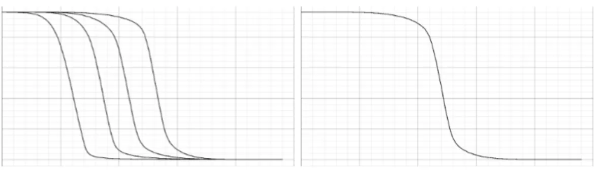
The robustness of a digital gate can be pointed out by the slope of its transfer function, since it determines the noise margins and the capability to regenerate a noisy input signal into a full-dynamic output signal.
In addiction, it must be considered that, due to the increased sensitiv-ity to parameter variations in weak inversion, it is more difficult to have a symmetric transfer function in a CMOS inverter (Figure 1.4(a)).
(a) Non symmetric TF (b) Symmetric TF
Figure 1.4: Transfer Function (TF)
It is however well known that good noise margin are obtained with a symmetrical transfer function (Figure 1.4(b)).
In a digital inverter the cross-over point is defined as the input voltage that should be applied to obtain an output voltage equal VDD
2 . At the cross-over point IDSn = IDSp, and VDSn =
¯ ¯VDSp ¯ ¯= VDD 2 . To obtain IDSn = IDSp,
for an inverter operating in subthreshold regime, the Wn Wp
ratio is typically different than in strong inversion.
Figure 1.5 shows the result of a simulation in CMOS 90nm technology node, displaying that in subthreshold region a symmetrical transfer function is given by Wn
Wp ≈ 1.
For this reason, a definition of new libraries for the subthreshold region operation is needed. Table 1.1 shows a comparison between a standard in-verter in strong inversion region, the same inin-verter in subthreshold regime
Figure 1.5: Symmetrical TF
and two different types of inverter optimised for the subthreshold operating region. The data refer to the CMOS 45 nm technology node.
Std. CMOS Optimised library
1.1 V 0.3 V
Wp = 215nm Wp = 120nm Wp = 200nm
Wn = 165nm Wn = 120nm Wn= 120nm
Max Freq (fmax) [MHz] 11.7e3 27.3 60.6 (+120 %) 58.9 (+115 %)
Power @ fmax [nW] 125e3 20.3 17.4 (-14 %) 21.57 (+6.2 %)
Switching Energy [ nWMHz] 10.6 0.74 0.28 (-61 %) 0.36 (-50 %) Table 1.1: Optimised inverter performance
has a huge performance decrease. On the other side, better results are ob-tained, in the same operating region, with a standard-like inverter having Wn = Wp.
More information on ULP design strategies can be found in [8], [9], [10], [11].
1.3
Testchip
This project aims to design and to realize a testchip to investigate and to quantify the improvement of the circuit performances obtained through the design of dedicated litho-friendly (LF) and of the Ultra Low Power (ULP) standard-like libraries. The LF standard cell libraries are optimised for lithography using ultra regular layout styles. The ULP standard cell library is optimised to operate at extremely low supply voltage.
The main objective of the testchip is to get insight into the local and the global variability of relevant parameters for digital design, such as operating frequency and power consumption. In this testchip some structures are also included, to develop some innovative circuits that should help to monitor the quality of the technology process. The testchip is realised in a CMOS 45 nm process.
The planned testchip is made up the following blocks:
• Main Cores: one for each of the five designed libraries, plus a rotated version of a lithofriendly library. Each core contains a combinatorial logic block to measure the statistical parameters of the circuit’s perfor-mances.
• Digital Core: a small digital core, where combinatorial and sequen-tial logic are implemented together, to verify the circuit behaviour at extreme low voltages.
• Process Monitors: to verify the quality of the process and of the impact of a lithofriendly design approach on the fabrication process.
A representation of the entire testchip is reported in Figure 1.6.
Figure 1.6: Top-level of the testchip and its modules
1.3.1
Target Performance Measurements
The aim of the circuit is the qualification of the realised standard cell li-braries. The quantities that have to be measured in these structures are the active power Pon, the standby-power Pof f of the circuits, the maximum
oper-ating frequency f , and the dependence of the active power on the operoper-ating frequency and the circuit activity. This testchip is designed to gain a strong insight about the robustness of digital circuits in nano metric devices. The mean (µ) and the standard deviation (σ) of these performance indicators are good measurements of circuit sensitivity to local and global variability.
To perform variability measurements, the basic structures realised on the testchip are ring oscillators (see Section 1.3.3). It is well known [5] that variability effects are mostly perceptible in the delay of the affected cell. Therefore, ring oscillators are used to attain statistical information on the delay of the cells composing them from frequency measurements. The operating frequency of a ring oscillator is given by:
f = 1 T = 1 2 N X i=1 τdi
Where T is the ring oscillator period, N is the number of cells composing the ring oscillator, and τdi is delay of the i-th cell, supposed to be
approxi-mately the same for the raise and fall commutation.
Given this relation, the mean value and the standard deviation of the ring oscillator period will be:
< T >=< 2 N X i=1 τdi >= 2 N X i=1 < τdi >= 2N < τd > (1.6) σT2 = 2N · στ2d and σT = √ 2N · στd (1.7)
For small relative variations, even if the relation between time and fre-quency is not linear, we have:
∆f f ≈ ∆T T Therefore: σf < f > ≈ σT < T > (1.8) From equations 1.6, 1.7 and 1.8 is then possible to find the relation be-tween the relative standard deviation of the measured frequency and of the delay time: στd < τd > =√σT 2N · 2N < T > = √ 2N ·< T >σT ≈√2N · < f >σf (1.9) The active power Pon depends on f . Both active and standby power Pon
and Pof f are a function of supply voltage VDD, back-bias voltages Vbbp and
Vbbn, and temperature T . Therefore, the following measurement are required:
• Pof f as a function of VDD, Vbbp, Vbbn, and T .
In the design of the circuit, the following requirements must be fulfilled: • Independent power supply connections for the different modules; • independent back-bias connections (pwell and nwell);
• controllable activity α of the digital block.
Statistical information on local variability, measurements of many identi-cal delay paths layouted at close distance are necessary. Statistiidenti-cal informa-tion on global variability is obtained by measuring different dies or samples. To gain further insight into lithography properties, at least one of the test cores should be placed twice with different orientations; therefore one of the instances rotated of 90 degrees.
1.3.2
Main Core modules
In the testchip there are six digital modules which perform the same func-tionality. They are realised with different standard cell libraries, optimised for different goals.
The aims of these digital cores are first of all to prove that the design methods used to implement the digital libraries are efficient, and then to quantify the gain in performance obtained with these optimised digital li-braries.
The modules are:
• Reference Std. Library Module (REF), implemented with the cells from the reference standard library currently available in the digi-tal flow. This module is implemented in the testchip to have a reference for the other modules in terms of power and frequency performance. • 3 Lithofriendly Library Modules (LF<1:3>), developed with three
different layout approaches. The main aim of these libraries is to im-prove the lithofriendliness of the design and therefore to reduce the
spread of the performance and to improve the yield of the digital cir-cuits (see Section 1.1.2).
1. LF1: lithofriendliness is limited to the active areas: all the transis-tors are drawn with the same width and length, thus the standard-like cells are higher than the standard one. The area overhead is the most significant.
2. LF2: lithofriendliness is extended to active area, poly and con-tacts. There is a small area overhead, and the metal layers are not designed for lithography.
3. LF3: lithofriendliness is extended to all layers. The performances are in this way decreased, but the reduced spread obtained in this way is expected to compensate the performance loss.
• Rotated Lithofriendly Library Module is a rotated copy of LF2, to verify the effect of orientation on the performances of the circuit. • Ultra Low Power Module (ULP) makes use of a digital library
optimised to operate at low voltage supplies (see Section 1.2).
The design of a large digital library is unfeasible with the limited available resources and it is not strictly necessary since the first goal of this project is the verification of the design concept. In this experiment the main design focus is limited to few combinatorial logic gates and to Flip-Flops. Although the limited number of cells, the measurement results can give a good insight of the trend of the performances of the digital logic that could be developed, if one of these libraries would be adopted in a real digital design. The key performances that are going to be observed in this experiment are maximum operating frequency, the power consumption and the robustness of these performances to process variations and device mismatch.
Each digital module is constituted by a C2-block: with this block the
up by four C-Blocks. The basic structures of these combinatorial blocks are ring oscillators.
1.3.3
Description of a C
2-Block
The C2 Block is the part of the core module where the combinatorial logic is
proven. It is made up by four C-blocks, each of them consisting in two arrays of 128 ring oscillators (RingOs). The C-Blocks differ for the logic gates with which the RingOs are realised, i.e. IVX, NAND, NOR or MXD.
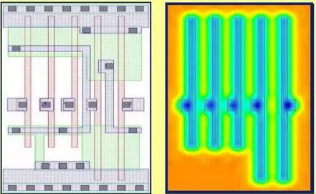
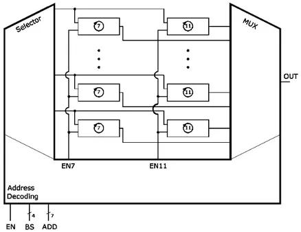
Beside the arrays of ring oscillator, each C-Block has also a selector and a multiplexer to complete its functionality. The selector enables the oscillation of the required RingO(s), while the multiplexer selects which output node has to be available at the output pad. In Figure 1.7, the high level schematic of a C-Block is reported.
Figure 1.7: Block diagram of the C-Block: RingO arrays and control logic In the following of this Section, a short introduction to the dimensioning of each part of this structure is given.
• Ring Oscillators: The basic structures of these combinatorial blocks are ring oscillators. They are developed with Inverter, with Nand, with Nor or with a mixture of these cells. To compare consistent data, in case of two inputs gates, the signal is sometime associated to the node closer to the output node. The logic depth of the ring oscillators, i.e. the number of combinatorial gates that are cascaded, has been determined as a trade off between two opposite conditions:
– On one hand, the logic depth of the RingO should be minimised, since one of the main aims of this experiment is to verify if the optimised libraries reduce the performance (i.e. gate delay and thus RingO operation frequency) spread. As the number of the cascaded elements within the ring oscillator increases, the perfor-mances of the single gates are averaged out.
– On the other hand, the oscillating frequency of a ring oscillator increases decreasing the number of cascaded gates. Since the max-imum acceptable frequency is limited by the maxmax-imum speed of the frequency divider that is connected between the RingO and the measurement equipment, depending on the speed of the single gate a lower border for the logic depth of the RingOs is found. For the given technology and the designed Flip-Flop, RingOs with a 7-logic depth satisfy the requirements above. Since this technology node is still not mature, RingOs with 11-logic depth are also realised to en-sure the functionality of the circuit also if the frequency of the circuit is above the expected corner situations. To attain a relevant number of measurements, and therefore to be able to derive some statistical in-formation about the spread, the number of RingOs must be sufficiently high. In this experiment 128 RingOs of each type are designed.
• Control logic: it is made up by a selector that decodes the addresses for the activation of the corresponding RingOs (see Chapter 3), and by a multiplexer that routes the output of the selected RingOs to the
output of the circuit (see Chapter 2). The inputs of the control logic are:
– 7-bit input Address (ADD < 6 : 0 >), which encode the selector line that has to be active.
– the enable signal (EN ) that identifies which array has to be ad-dressed;
– 4-bit input Block Select modes (BS < 3 : 0 >), active low, which functionality is reported in Table 1.2;
– Disable signal (DIS): that turns off the entire block.
Since the multiplexer must report to the output the signal of the ring oscillator enabled by the selector, the selector and the multiplexer may share the same address decoding logic. The output of the multiplexer presents a high frequency signal. The output signal is therefore sent to a frequency divider and afterwards to the output pad.
In the normal state, the selector enables only one of the 2x128 RingOs to oscillate, while the others are in the disable condition. Modifying the value of the address bits, all RingOs can be activated one after the other and the operating frequency of each of them can be measured at the output node of the multiplexer.
The selector presents also some special modes, which are coded through the Block Selector (BS) inputs. The aim of these special modes is to enable the simultaneous oscillation of more RingOs. When the circuit operates in these modes, the main goal is to measure the power con-sumption as a function of the circuit activity, while there is no interest to observe the output voltage of the multiplexer.
In Table 1.2 the special modes of the selector and the value of the control inputs are reported. Since the EN signals may never be active together, i.e. the 7-depth RingOs array can not be activated together
with the 11-depth RingOs array, the selector functionality is illustrated with just one EN signal.
Mode Control bits
(Activity) DIS BS3 BS2 BS1 BS0 Normal 0 1 1 1 1 25% 0 1 1 1 0 50% 0 1 1 0 0 75% 0 1 0 0 0 100% 0 0 0 0 0 0% 1 X X X X
Table 1.2: Special modes for the selectors
• Scan chain: it is a structure of shift registers with serial input and serial output, whose information is loaded from an output pad during the initialization phase of the testing, and determines part of the test vectors. In this test structure, the information that can be stored in the scan chain is the value of the address, the value of the BS and the value of the DIS signal, i.e. 15 bits per module.
A C2-Block is obtained joining four C-Blocks (Figure 1.8). During the
measurement at most one of the four C-Blocks must be active. To save some silicon area, the C-Blocks of each digital module may share the address lines, the BS and the EN signals, while the DIS signals differ for each C-Block.
The routed signals in the C2-block are therefore:
• ADD<9-0>: 7 Address + 3 coded DIS = 10 bits Address; • BS<3-0>: Block select modes (active low);
Figure 1.8: Block diagram of the C2-Block
I/O and Pins of the ring oscillators module The I/O signals of each module are:
• VDD: supply voltage for RingOs
• VDDS: pMOSFET bulk connection for RingOs
• VSS: ground for RingOs
• VSSS: nMOSFET bulk connection for RingOs
• VDDH: supply voltage for control logic
• VSSH: ground for control logic
• SI: Input of the scan chain • SO: Output of the scan chain
• CLKs: Clock signal of the scan chain
Each main core needs separate supplies voltage pins to ensure a complete independence of the blocks during the power consumption measurements. Each module must present also a separate OUT pin.
There are three choices for the scan chain:
1. a safe choice is to reduce the length of the scan chain, so that each module has its own, that would require 3 pins, for a total of 18 pins; 2. 5 pins could be saved sharing the same clock signal for all the scan
chains (CLKs);
3. if the number of available pins is limited the scan chain of all modules is just one, and the only 3 pins are necessary for the six modules. This solution has as drawback the fact that the scan chain must connect block that may be placed at a relative quite large distance in the chip. In Table 1.3 the number of I/Os and of PINs for each module and the total for all six modules is reported. Between bracket are the value needed to realise alternative solutions that ensure the same logical functionality and the same measurement capability, but which are more complex in the layout phase, and therefore may introduce more risks in the realisation.
1.3.4
Digital Core
In Section 1.2.1 the basic principles of the subthreshold regime are given. Moreover, it is discussed how an optimised design strategy is necessary to improve the performance of circuits operating in subthreshold region.
Table 1.1 points out how, for the inverter performance, standard cells can be optimised to give better results in subthreshold regime.
I/Os PINs VDD 1 6 VDDS 1 6 VSS 1 6 VSSS 1 6 VDDH 1 6 VSSH 1 6 SI 1 6(1) SO 1 6(1) CLKs 1 6(1) OUT 1 6 TOTAL 10 54(49-39) Table 1.3: I/O and Pins of the RingOs
However, since power consumption in handheld systems is one of the most significant constraints, all strategies leading to energy saving are explored. It is an emerging idea to make these systems work at low frequencies in subthreshold regime when they are in idle, lowering their VDD.
In Chapter 4 the digital core design is discussed. In the digital core realised on the testchip, standard combinatorial and sequential logic are im-plemented together. The aim of this core is to verify how a circuit designed to work in strong inversion region behaves at extreme low voltages.
1.3.5
Process Monitors
In Section 1.1 the main problems of the design scaling are discussed. More-over, in Section 1.1.2 the lithofriendly approach is introduced. For the new technology nodes, such as the CMOS 45nm used in this project, the actual advantages and drawbacks of a lithofriendly design approach are still to be quantified.
out the actual reliability and robustness of the process itself, and to point out the necessity to adopt litho-driven design methodologies. The task of the monitor is to verify the presence of a systematical error introduced by pattern aberrations.
In Chapter 5 the design of analog process monitor is discussed.
1.3.6
Test setup considerations
Considerations about the available test facility:
• Maximum 8 power supplies available at the same time. Two are re-quired for the pad ring, so 6 are left for the cores on the test chip. • Maximum realistic input signal frequency = 500 MHz.
• Maximum realistic output signal frequency = 100 MHz. • PGA package with up to 256 pins is preferred.
Multiplexer
A multiplexer, or mux, is a circuit used to select one out of many analog or digital data sources and to output that source into a single channel. This process is called multiplexing.
A multiplexer is an ideal multi-input, single-output switch. A signal called selector specifies which one of the multiple inputs has to be forwarded to the output.
A multiplexer with N inputs needs M selector bits, where 2M ≥ N.
In Figure 2.1 a 2 inputs, 1 output multiplexer (2x1 mux) is shown. Thus, in this case, N = 2 and M = log2(N ) = 1.
Figure 2.1: 2x1 multiplexer
In this Chapter the design of a multiplexer is discussed. In Section 2.1 the project requirements for this work are analysed. In Section 2.2 an overview of the basic mux core cells is given. In Section 2.3 different multiplexer archi-tectures are analysed, and the choice of an architecture fulfilling the project requirements is discussed. Then, a performance comparison between
plexers based on different core cells is given in Section 2.4, using simulations results. Section 2.5 deals with a modification of the project specs, adopted to reduce the area occupation of a mux, hence not decreasing its performances. In Section 2.6 the performance modifications given by a technology change are presented. Section 2.7 shows the effects of the parasitic parameters on the multiplexer performance.
2.1
Project requirements
In each C -block two arrays of 128 ring oscillators are present: one made up by 7 logic depth RingOs and the other by 11-logic-depth RingOs. The oscillation frequency for a 7-logic-depth RingO is about 5 GHz in the typical case, and can range from about 1.4 GHz to 10 GHz in the corner cases. The frequency of the 11-logic-depth RingOs is lower and thus non critical.
In this project, a 128x1 multiplexer is required to select one out of 128 ring oscillator outputs for each array. The main aim of the multiplexer is to forward the selected signal without frequency distortions. The capability to achieve this target in different conditions is called robustness. The realisation of a robust multiplexer in the mentioned frequency range and for the adopted supply voltage (1.1 V) is vital for this project. It has to be noticed that the selection signals are at low frequency, therefore the critical signals for the ro-bustness are the mux inputs only. Alongside the roro-bustness, area occupancy and power consumption are considered among the multiplexer performances, and their reduction has to be achieved.
Since N = 128, M = log2(128) = 7 selection bits are needed. These bits are decoded in order to obtain 128 mutually exclusive signals: when one of them is active the remaining 127 must be inactive. Since the 7 and the 11 logic depth RingOs are never active at the same time, the multiplexers for the 2 arrays have the same structure, and share the same selection bits. For this reason they will be hence no more considered separately.
Moreover, the 7 selection bits are the same arriving to the selector block. Therefore the decoding logic between the two blocks may be shared, routing
the 128 mutually exclusive signals from the selection block to the multiplexer (Figure 2.2). This solution is justified by the proximity of the selector to the multiplexer.
Figure 2.2: Share of the address decoder
After the multiplexer stage, a frequency divider is realised to attain a factor thousand division of the signal frequency. In this way, the frequency of a signal forwarded to a pad fulfills the requirement of the measurement equipment in any operating condition.
2.2
Switch element
As mentioned above, an ideal multiplexer is nothing more than a multi-input switch. Different circuit realisations of multiplexers exist, depending on the way the switch function is implemented.
The core element of the multiplexer is the switch element: depending on the value of its selection signal, its input signal can be either forwarded toward the output or cut off. All outputs of the switch elements are connected together at the multiplexer output. For this reason, when a switch element is inactive, it must not drive the output. The switch cell must thus have the possibility to set its output to a floating mode.
In this project two different types of multiplexer are taken into account. They have the same structure, but they differ in the switch element. The two used switch elements are the Pass Gate and the 3-State Buffer.
2.2.1
Pass Gate
A Pass Gate is made up by a pMOS and an nMOS transistor whose drains and sources are connected together (Figure 2.3).
(a) Symbol (b) Schematic
Figure 2.3: Pass Gate element
When the selection bit S is high, the channel of both pMOS and nMOS transistor is formed, thus the input I and the output O can be roughly con-sidered shorted. When the selection bit is low, none of the MOS transistors has a |VGS| > |VT|, therefore the input I and the output O are open-circuited,
and the O node can be considered floating.
The logic functionality of a Pass Gate is displayed in Table 2.1. I S O
0 0 Z 1 0 Z 0 1 0 1 1 1
Table 2.1: Pass Gate logic functionality
A Pass Gate 8x1 multiplexer, simulated in a 45 nm CMOS technology, operates correctly up to 5 GHz with nominal supply voltage of 1.1 V and minimum size transistors (W =120 nm and L =40 nm).
Since the Pass Gate gain is always equal or smaller than 1, its input signal cannot be enhanced. For this reason, using Pass Gates as switch elements
for the multiplexer does not guarantee high robustness.
On the other side, this is the solution assuring the lower area occupancy, since each switch element is constituted by two minimum dimension transis-tors only.
2.2.2
3-State
A simple way to realise a 3-State Buffer is shown in Figure 2.4: the two MOSFETs closer to the output node (nMS and pMS) are driven by the selection bit S (nMOS) and the negated selection bit ¯S (pMOS); the two MOSFETs next to the power rails (nMI and pMI) are driven by the input signal I.
(a) Symbol (b) Schematic
Figure 2.4: 3-State Buffer element
When the selection bit S is high, nMS and pMS can be considered as closed switches, and the circuit behaves like a simple CMOS inverter driven by the input I, whose output is O. When the selection bit S is low, nMS and pMS are approximately open switches, and the output O is floating.
The logic functionality of a 3-State Buffer is displayed in Table 2.2. The 3-State Buffer described above is just an inverter (given by nMI and pMI) driven by a high frequency signal, and two cascaded switches (nMS and pMS) driven by a low frequency signal. The critical part for robustness is thus the inverter: a correct dimensioning for nMI and pMI is vital. Through
I S O 0 0 Z 1 0 Z 0 1 1 1 1 0
Table 2.2: 3-State Buffer logic functionality
simulations it has been noticed that good results were obtained by having WpM I ≃ 1, 414 · WnM I, where WnM I and WpM I are respectively nMI and pMI
widths.
The 3-State Buffer gain is gmMI
gmout, with gmout directly dependent on WM S.
With these transistor dimensions, the 3-State Buffer gain is greater than 10dB. Therefore, when a signal is selected through a 3-State Buffer multi-plexer, its logic levels are restored.
Unfortunately, the higher robustness of this solution is paid in area: this switch element requires 4 transistors instead of the 2 needed by the Pass Gate, and they may not be at minimum size. To achieve the required speed the total area is greater than two times the Pass Gate area.
This solution requires also supply power, while the Pass Gates are passive circuits, disconnected by the power rails.
2.3
Multiplexer architecture
In this Section different multiplexer architectures are analysed. For each one of these architectures advantages and drawbacks are pointed out. In particular, the architecture analysis focuses on the capability to fulfill the requirements of this project.
In Section 2.1 it has been mentioned that the robustness of a mux can be evaluated as its capability to forward the selected signal without frequency distortions. A limitation to the multiplexer robustness is given by the maxi-mum capacitance drivable by a single switch element.
Since the RingOs operating frequency is known, the maximum drivable load capacitance of a single switch element is determined through simulations at that very frequency. The results below showed are obtained using Pass Gates as switch element.
Figure 2.5 shows that for a CL≥3.5 fF the Pass Gate multiplexer output
is less than 90% of the amplitude of its input. Since the nMOS and the pMOS transistors have the same dimensions, this loss is asymmetrical for the high and the low logic level of the signal, as shown in Figure 2.6. Thus the value of 3.5 fF is way too high.
Figure 2.5: Output signal dynamic amplitude vs. load capacitance Figure 2.6 shows that, at the operating input frequency, the output wave-forms have acceptable values of both maximum and minimum amplitudes for a load capacitance lower than 2.5 fF. For the 3-State Buffers very similar re-sults are obtained.
In the following, for the discussed architectures the value of the output capacitance is derived, in order to evaluate their reliability.
hier-Figure 2.6: max[Vout]
VDD and
min[Vout]
VDD vs. load capacitance
archical architecture (Section 2.3.1) and a multi stage or hierarchical archi-tecture (Section 2.3.2).
In Section 2.3.4 and 2.3.3 possible modifications to further improve the hierarchical architecture functionalities are discussed.
2.3.1
Single array
The simplest method to realise a multiplexer is to connect the output of all the switch elements at the output of the multiplexer. This solution is known as non hierarchical mux or single array mux.
If the multiplexer is organised as an array of N elements (Figure 2.7), the load capacitance for a single switch element is given by the parallel of the output capacitances of the N switch elements plus the load of the following stage. Therefore:
Figure 2.7: Array of N switch elements (Pass Gates)
If a Pass Gate switch element is chosen, the capacitance at the output of a single element (COU TP G) is mainly given by the parallel of the two
Drain-to-Body capacitances of its nMOS and pMOS transistor. Thus:
COU TP G≈ CBDn+ CBDp ≃ CJLc(Wn+ Wp) = 2 · CJLcWmin
Where CJ (the junction capacitance) and Lc (the contact length) can be
considered, in first approximation, technology defined parameters.
through a Spectre simulation, is ca. 200 aF; while the total output capaci-tance C′
Lof the unloaded mux results ca. 24.5 fF, thus close to the theoretical
value C′
L= 128 · COU TP G ≃ 128 · 0.2 fF = 25.6 fF.
Since the capacitance at the output of a 3-State Buffer is comparable to the Pass Gate one, and since it is no critical to have the inner transistors (nMS and pMS) at minimum width (Wmin), COU TP G ≈ COU T3SB. For this
reason, there is no evident advantage in the load capacitance value using the Pass Gate solution rather than the 3-State Buffer one.
The value found for C′
Lis more than 10 times higher than the 2.5 fF limit.
Therefore, despite its simplicity, a non hierarchical solution is unacceptable in this technology node for a 128x1 multiplexer.
2.3.2
Multi stage
Due the load capacitance limit, a hierarchical architecture for the multi-plexer has been adopted. The mux is redesigned with more than one stage. Figure 2.8 shows the case of 3 cascaded stages.
Adopting a hierarchical architecture increases the multiplexer area, and makes its structure more complicated. Both these effects get worst as the number of stages increases. On the other hand, having more than one stage reduces the dimensions of the single stage components, and thus their capac-itances. Moreover, a hierarchical multiplexer is controlled through a hierar-chical addressing. Therefore it is no longer necessary to route the N = 128 selection signals from the decoder realised in the selector to the mux (Fig-ure 2.2). The number of signals to route depends on the chosen architect(Fig-ure. Two stages mux
First, let us consider a 2 stages 128x1 multiplexer, made up by 16 8x1 mux (first stage) whose outputs are connected to a 16x1 mux (second stage).
In this case, to perform the selection, 8 mutually exclusive signals (or 3 coded bits) are needed for the first stage and 16 for the second stage. The number of signals to be routed from the selector is thus 24.
The load capacitance for the first stage results:
CL= CL′ + CEXT = CL1 ststage + Cin2 ndstage = 16 · COU Tse+ Cin2 ndstage ≃ ≃ 16 · 0.2 fF + 0.5 fF = 3.7 fF
Even if the value of CL is lower than for the single array multiplexer, it
is still too high to be driven by a signal at the required operating frequency. Therefore, a two stages multiplexer does not fit the requirements.
Three stages mux
A three stages hierarchy is then considered. The chosen hierarchical archi-tecture is 4x4x8:
1. The first stage has 128 inputs and 32 outputs. It is made up by 32 4x1 muxs.
2. The second stage has as inputs the 32 outputs of the previous stage, and it has 8 outputs. It is made up by 8 4x1 muxs.
3. The third stage has as inputs the 8 outputs of the previous stage, and it generates the output of the entire 128x1 multiplexer. This stage is just one 8x1 mux.
In this case, to perform the selection, 4 mutually exclusive signals (or 2 coded bits) are needed for the first stage, 4 for the second stage, and 8 for the third stage. The number of signals to be routed from the selector is thus 16.
The critical stage for the load capacitance is the last one, since is there that the highest value of C′
L is found:
C′
L= 8 · COU Tse ≃ 8 · 0.2 fF = 1.6 fF
that is less than the 2.5 fF limit. A three stage multiplexer thus fits the requirements.
2.3.3
Standard library multiplexer
Alongside the two main solutions (Pass Gate mux and 3-State Buffer mux), another multiplexer type has been taken into account in the performance evaluation. This multiplexer type is a standard library cell, based essentially on 3-State Buffers. The standard cell is a 4x1 mux, counting 20 transistors (Figure 2.9). It is important to notice that the choice of a 4x1 multiplexer fits the requirements of the 4x4x8 hierarchical architecture discussed above. From Figure 2.9 can be seen that the operative principle of the standard cell mux is the same of a 3-State Buffer mux. The selection signals are S0 : S3; the inputs are D0 : D3. The main advantage of this solution is given by the area reduction obtained by a clever logic minimization. For this cell, there is no need to have both the select and the negated select signals to activate a path, as it happens in the Pass Gate and the 3-State Buffer cells shown in Figures 2.3 and 2.4.
Figure 2.9: Standard cell: 4x1 mux Area occupancy
A rough evaluation of the area occupancy of a 4x1 mux can be given counting the number of its transistors. Table 2.3 shows the total number of transis-tors for the three solutions, considering the inverters needed to negate the selection signals (4 for the 3-State Buffers and the Pass Gates, none for the standard cell) and the ones to regenerate the output signal (1 for the 3-State Buffers and the Pass Gates, 2 to take in account the NAND of the standard cell).
Switch elements FETs per se Inverters Total
Pass Gate 4 2 5 18
3-State Buffer 4 4 5 26
Std Cell 4 4 2 20
Table 2.3: Number of transistors for a 4x1 Mux
It is then possible to realise a hybrid multi stage multiplexer, using the 3-State based standard cells for the first and the second stage to ensure robustness, and a 8x1 Pass Gate mux for the last stage to minimize size.
2.3.4
Frequency Divider mux
Several simulations have been run to compare the multi stage multiplexers based on Pass Gates, on 3-State Buffers and the hybrid multiplexer.
In the typical case simulations (TT), all 3 solutions give comparable re-sults. In the corner simulations (FF and SS), the Pass Gate evidences its lower robustness.
Although all 3 architectures present an output waveform with acceptable amplitude, duty cycle and correct frequency, further architectures have been investigated to obtain a multiplexer closer to the ideal functionality.
In the three stage mux, the last stage is the critical one for the output capacitance value, and thus is the one that can more distort the signal.
It has been mentioned in Section 1.3.3 that the frequency of the mux output must be divided by a factor thousand in order to fulfill the require-ments of the measurement equipment. For this reason a frequency divider is present. It can be implemented by the cascade of 10 Flip-Flops.
Since the output of a Flip-Flop is a square wave with duty cycle δ = 50% and half the frequency of its input, a FF could be used to regenerate the signal before the third stage of the mux. Therefore, a stage of Flip-Flops may be inserted before the last stage of the multiplexer.
The circuit thus obtained is called Frequency Divider multiplexer (FD mux), and performs the multiplexing and a factor 2 division of the input signal frequency.
With a FD mux, the input signals of the third stage, the critical one, are completely regenerated and their frequency is halved.
In Figure 2.10 a comparison between the last stage waveforms of a three stage multiplexer and a three stage FD mux is given. Both multiplexers use 3-State Buffers as switch elements. The data shown below are obtained in a typical case simulation (TT), thus the driving signal frequency is about 5 GHz.
Even in the more robust solution, the 3-State Buffers multiplexer, the advantages in robustness given by the FD mux are perceptible. Using a FD
(a) Mux: 3rd stage input (b) FD mux: 3rd stage input
(c) Mux: 3rd stage output (d) FD mux: 3rd stage output
Figure 2.10: Comparison between a Mux and an FD mux
mux the multiplexer output is a rail-to-rail signal, with δ ≈ 50%, and smaller raise and fall times. None of these characteristics is reached in a simple three stage mux.
The advantage of this architecture is that it makes the last stage not critical for the mux functionality.
The FD mux architecture has been therefore adopted.
The main drawback of this architecture is that, since a Flip-Flop is needed before each of the 8 inputs of the last stage, it occupies a slightly larger area.
2.4
Performance comparison
In Section 2.3.4 the choice of a 4x4x8 multiplexer with a factor 2 frequency divider before the last stage was discussed. Defined the architecture, 3 paths can be followed in the realisation of the multiplexer, depending on the used switch element:
1. Pass Gate multiplexer; 2. 3-State Buffer multiplexer;
3. Hybrid multiplexer, using the 3-State based standard cells for the first and the second stage, and a 8x1 Pass Gate mux for the last stage. Among the evaluated performances, in this Section a comparison between the three solutions is carried out taking into account the following features:
• input/output functional bound;
• variability introduced by the multiplexer itself; • area occupation;
• power consumption.
The choice of the switch element, based on this comparison, is discussed in Section 2.4.5.
2.4.1
I/O bound function
Because of the insertion of a factor 2 frequency divider before the last stage, the three stage FD mux is no longer a linear system. For this reason, its behaviour can no more be described by a transfer function. Nonetheless, it is possible to derive a functional relation between the input and the output signals of the multiplexer. In particular, the relation between input and output frequencies has been hence defined bound function.
For the 3 solutions the bound functions are derived in the typical case (TT), to evaluate their reliability. It is useful to remind that the nominal frequency of a 7 stages ring oscillator is about 5 GHz.
(a) Pass Gate mux (b) 3-State Buffer mux
(c) Hybrid mux
Figure 2.11: I/O bound functions for the 3 solutions
From Figure 2.11, it can be seen that between the input and the out-put frequencies a linear relation exists. This relation is maintained in a bandwidth that is approximately the same for the 3 solutions: up to about 6.7 GHz for the Pass Gate and the 3-State Buffer multiplexers, and up to about 6.1 GHz for the hybrid mux. The slope factor of the bound functions is 1/2, due to the frequency divider.
2.4.2
Variability
As mentioned in Chapter 1, among the aims of this project there is the measurement of the process variability, to investigate solutions that may reduce the spread of technology parameters. This analysis is carried out through the design of ring oscillators and Flip-Flops. For the RingOs, the statistical distribution of the parameters spread may be estimated through the analysis of their oscillating frequency.
The multiplexer must only select the signal generated by one of the ring oscillators, and forward it to a pad, in order to have it available for the fre-quency measurement. From the signal frefre-quency is then possible to quantify the average variations of the delay of the gates making up the ring oscillators. Therefore the mux must not introduce unwanted variations to the output frequency of the oscillation that has to be measured.
To quantify the variations introduced by the different multiplexer types, Monte Carlo simulations are used. Based on the bound functions shown in Figure 2.11, the behaviour of each multiplexer is simulated in 5 points, given by the following input frequencies: 2 GHz, 3.5 GHz, 5 GHz (the expected operating frequency), 5.3 GHz and 6 GHz.
For each point, 500 iterations are carried out to obtain an acceptable statistical significance.
The result of each of the 15 Monte Carlo simulations (5 points for each of the 3 solutions) is a stochastic distribution. The data obtained are shown in Table 2.4.
From the distribution mean value µ and standard variation σ, the relative variability σ
µ is derived.
At the operating frequency of 5 GHz all 3 solutions present a very low variability: σ
µ < 77ppm.
At lower frequencies the results are even better.
At 5.3 GHz variability is proved to be still very low: σ
µ < 94ppm.
At 6 GHz the introduced variations are unbearable, since this frequency is the closer to the upper limit of the FD mux, especially in the hybrid case
2 GHz 3.5 GHz 5 GHz 5.3 GHz 6 GHz µ [GHz] 0.9999999 1.75 2.4999999 2.6500055 2.9244825 PG σ [Hz] 3788.5 3463.9 1611.1 126.68e3 275.6e6 variation 3.8 ppm 2 ppm 0.6 ppm 47.8 ppm 9.4% µ [GHz] 0.9999969 1.7499956 2.499993 2.6499925 2.9315076 3SB σ [Hz] 4992.7 5048.7 5904.2 6646.6 260.102e6 variation 5 ppm 2.9 ppm 2.4 ppm 2.5 ppm 8.9% µ [GHz] 1.0000002 1.7500001 2.4999909 2.650006 2.7805446 Hybrid σ [Hz] 3522.7 2653.9 191.74e3 248.24e3 450.464e6
variation 3.5 ppm 1.5 ppm 77 ppm 93.7 ppm 16.2% Table 2.4: Monte Carlo simulation results
(Figure 2.11). Nonetheless, since simulations proved that the frequency of the ring oscillators varies in a very small range around its operating point (about 5 GHz±3%) in the typical case, the results at 6 GHz are not of major concern.
Even if at the nominal operating frequency the variations introduced by the hybrid FD mux, the worst performing one, are 130 times larger than the results obtained with the Pass Gate FD mux, their effect on the output signal is much lower than the variations introduced by the RingOs. Therefore, at this stage, all 3 solutions are still available.
2.4.3
Area occupation
A common way to estimate area occupation for digital circuits is to count the number of transistors.
In Table 2.3 the number of transistors needed to realise a 4x1 multiplexer in the 3 different solutions is quantified.
In Table 2.5 the same count is carried out for a 128x1 FD mux. The amount of switch elements (3SB: 3-State Buffer; PG: Pass Gate; Std: stan-dard 4x1 mux), Flip-Flops (FF) and inverters (IVX) is quantified. The num-ber of transistors for each element is reported between brackets. In the last column the total number of transistors for each mux solution is calculated.
Switch elements Logic
PG (2) 3SB (4) Std (20) IVX (2) FF (26) Tot Pass Gate 168 0 0 330 8 1204 3-State Buffer 0 168 0 490 8 1860
Hybrid 8 0 40 168 8 1360
Table 2.5: Number of transistors per multiplexer
To count the number of inverters, both the ones needed to regenerate the signals between the stages and the ones to negate the selection bits are taken into account. As expected, the Pass Gate solution guarantees the lower area occupation. For the hybrid solution, since the negated selection bits are no needed, the area is slightly higher than for the Pass Gate solution, but still much lower than for the 3-State Buffer mux.
2.4.4
Power consumption
The power consumption for a single path through the multiplexer is simu-lated. The power from the supply voltage is evaluated apart from the power absorbed from the ring oscillator (Table 2.6)
Supply [µW] RingO [µW] Total consumption [µW] Pass Gate 161.47 5.389 166.859
3-State Buffer 189.68 0.165 189.845 Hybrid 175.12 0.805 175.925
Table 2.6: Power consumption for a single multiplexer path
The trend results to be very similar to the one found for the area, since the total power consumption raises as the number of transistor increases.
It can be observed that the Pass Gate solution, although is the least consuming, absorbs more power from the ring oscillators than the other so-lutions. This is due to the intrinsic nature of the Pass Gate, that does not regenerate the input signal, but brings it directly to the output. Subtracting
current from the ring oscillators could affect their frequency and even prevent them from oscillating. Thus,the robustness of the Pass Gate mux must be verified in the worst case corner.
On the other side the 3-State Buffer solution needs almost no power from the ring oscillators, but absorbs more power from the supply pin than the other solutions.
As for the area occupation, the hybrid solution is a trade off between the other ones.
2.4.5
Switch element choice
As mentioned before the 3-State Buffer FD multiplexer is more robust than the Pass Gate FD mux, especially in the corner cases (FF and SS). On the other side, Pass Gate FD mux proved to be better in area occupation and supply power consumption.
Between these two solutions, the hybrid FD multiplexer resulted to be almost as robust as the 3-State Buffer one, since is also based on 3-State elements, but less area and power consuming. Therefore, for the multiplexer realisation, a hybrid solution is adopted, using the 3-State based standard cells for the first and the second stage, and a 8x1 Pass Gate mux for the last stage.
2.5
One mux per C -Block
In this Section, a possible modification of the project specifications is dis-cussed, in order to reduce the area occupation of the multiplexer, without decreasing its performances.
For each C -Block two arrays of 128 ring oscillators are present: one composed by 7 logic depth RingOs and the other one by 11 logic depth RingOs. To select one out of the 128 oscillators a FD multiplexer per array is implemented. The block diagram of the circuit is shown in Figure 2.12.
Figure 2.12: Block diagram of the C -block
one oscillation out of the 256 coming from the 2 arrays. A 256x1 FD mux can be designed combining the two 128x1 FD mux described above. This solution would save a large part of the logic block and one output pad.
The two possible architectures to implement the 256x1 FD multiplexer are:
1. 2x4x4x8 FD mux: modify the hybrid 4x4x8 FD multiplexer adding 256 Pass Gate as first stage;
2. 4x4x4x4 FD mux: completely based on the standard cell (4x1 mux). The area estimation for the two solutions clearly point out the advantage of the first one (Table 2.7).
PG (2) Std (20) Tot 2x4x4x8 mux 256+8 40 1328 4x4x4x4 mux 0 85 1700 Table 2.7: Number of transistors per multiplexer
Moreover, the adoption of a 4x4x4x4 solution unable the sharing of the selector decoder, since it is designed for a 4x4x8 multi stage architecture. On the contrary, switching from the 4x4x8 to the 2x4x4x8 architecture is very simple, since the first stage may be driven by the ENL and ENR bits, with
no need of additional logic.
Thus, only one 2x4x4x8 hybrid FD multiplexer per C -Block is realised. It is implemented with 128 2x1 Pass Gate mux as first stage, the 3-State based standard cells for the second and the third stages, and a 8x1 Pass Gate mux for the last stage (Figure 2.13).
Figure 2.13: Realisation of the 2x4x4x8 FD mux, modifying the 4x4x8 As discussed in Section 2.4.4, realising the first stage with Pass Gates as switch elements could decrease the mux robustness, since the power absorbed from the RingOs could prevent them from oscillating. Nonetheless, simula-tions proved that the 256x1 FD mux has no decreased functionality, and the overall robustness is guaranteed by the intrinsic robustness of the standard cells constituting the second and the third stage.


![Figure 2.6: max[V out ]](https://thumb-eu.123doks.com/thumbv2/123dokorg/7333979.91152/42.892.276.711.187.584/figure-max-v-out.webp)

