Universit`
a degli Studi di Ferrara
DOTTORATO DI RICERCA IN
MATEMATICA E INFORMATICA
Ciclo XXI
Coordinatrice: Zanghirati Luisa
Monte Carlo Simulations of Spin Glasses on
Cell Broadband Engine
Settore Scientifico Disciplinare: INF/01
Dottorando: Tutori:
Dott. Belletti Francesco Dott. Schifano Sebastiano Fabio
Prof. Tripiccione Raffaele
Abstract
Several large-scale computational scientific problems require high-end computing systems to be solved. In the recent years, design of multi-core architectures delivers on a single chip tens or hundreds Gflops of peak computing performance, with high power dissipation efficiency, and it makes available computational power previously available only on high-end multi-processor systems.
The aim of this Ph.D. thesis is to study the capability of multi-core processors for scientific programming, analyzing sustained performance, issues related to multi-core programming, data distribution, synchronization, in order to define a set of guideline rules to optimize scientific applications for this class of architectures.
As an example of multi-core processor, we consider the Cell Broadband Engine (CBE), developed by Sony, IBM and Toshiba. The CBE is one of the most power-ful multi-core CPU current available, integrating eight cores and delivering a peak performance of 200 Gflops in single precision and 100 Gflops in double precision. As case of study, we analyze the performances of CBE for Monte Carlo simulations of the Edwards-Anderson Spin Glass model, a paradigm in theoretical and condensed matter physics, used to describe complex systems characterized by phase transitions (such as the para-ferro transition in magnets) or model “frustrated” dynamics.
We descrive several strategies for the distribution of data set among on-chip and off-chip memories and propose analytic models to find out the balance between computational and memory access time as a function of both algorithmic and ar-chitectural parameters. We use the analytic models to set the parameters of the algorithm, like for example size of data structures and scheduling of operations, to optimize execution of Monte Carlo spin glass simulations on the CBE architecture.
Contents
Introduction III
1 Multi-core Architectures 1
1.1 The Raise of Multi-Cores . . . 1
1.2 Toward Many-Cores . . . 5
1.3 Multi-Core Architectures in 2008 . . . 5
1.3.1 Cell Broadband Engine . . . 7
1.3.2 Intel Nehalem . . . 20
1.3.3 AMD Shangai and Istanbul . . . 20
1.3.4 NVIDIA GT200 . . . 20
1.3.5 AMD ATI RV770 . . . 22
1.3.6 Many-core: Intel Larrabee . . . 22
1.4 Conclusions . . . 23
2 Spin Glasses 25 2.1 The Edward-Anderson Model . . . 27
2.2 Metropolis Algorithm . . . 29
2.3 The Binary Model . . . 30
2.3.1 Data and Operations Remapping . . . 32
2.3.2 Asynchronous Multispin Coding . . . 34
2.3.3 Synchronous Multispin Coding . . . 38
2.3.4 Mixed Multispin Coding . . . 38
2.4 Gaussian Model . . . 38
2.5 Conclusions . . . 39
3 Spin Glasses on Multi-Core 41 3.1 An Abstract Multi-core Architecture . . . 42
3.2 Data Structures . . . 43
3.3 Local Memory Version . . . 49
3.3.1 Synchronization . . . 53
3.4 Main Memory . . . 54 I
3.6 Conclusions . . . 61
4 Spin Glasses on CBE 63 4.1 Core implementation . . . 64
4.1.1 Data Parallelism and SIMD-Granularity . . . 66
4.1.2 Data Layout . . . 68
4.1.3 Random Number Generation . . . 79
4.1.4 Local Memory: Computational Core . . . 91
4.1.5 Main Memory: Performance and Data Access . . . 101
4.1.6 Memory Usage . . . 102
4.2 Interaction Between Cores . . . 104
4.2.1 Local Memory Version . . . 106
4.2.2 Main Memory Version . . . 108
4.3 Gaussian Model . . . 109
4.4 Conclusions . . . 110
5 Spin Glasses Performance on CBE 117 5.1 Binary Model . . . 117
5.1.1 Local Memory . . . 117
5.1.2 Main Memory Version . . . 121
5.1.3 Performance Comparison . . . 125
5.2 Gaussian Model . . . 128
5.3 Conclusion . . . 133
Conclusions 139
Introduction
Several large-scale computational scientific problems require high-end computing systems to be solved, or in some cases the development of “application-driven“ machines, custom-designed computing systems optimized for the resolution of a specific problem.
The huge amount of computational requirements and data to be processed have made until the recent past years very hard, and sometimes impossible, the use of commercial High Performance Computer (HPC) based on available standard com-puting technology.
Typical examples of such applications comes from several scientific fields like Earth Sciences (weather forecast, oceanography), Atrophysics (study of large-scale structures), Quantum Physics, Fluidodynamics, Biology, Molecular Dynamics [1, 2]. The request of an high computational power raises from the large scale of the events that have to be studied, and by the accuracy of the results to be achieved. Some of such applications are defined as Grand Challenge Problems, which means that with the actual technologies they may require years to be solved [3].
In the past, to solve this kind of problems two main categoires of computing systems have been used: general-purpose HPC commercial systems and special-purpose machines usually developed by research university groups. For example, for applications like weather forecast or biology, computing systems like the Cray machines and the IBM Power parallel systems have been extensively used with reasonably performance. General purpose systems are designed to be used for a wide range of applications, even for irregular applications where computing and communication patterns can change dynamically.
For other interesting scientific application this approach has not been sufficient and it required the design of specific computing architectures optimized for a par-ticular application. A typical example of such applications is the Lattice Quantum Chromodynamics (LQCD) which has triggered the development of several gener-ations of massively-parallel machines like the APE family in Europe [4] and the Columbia University systems, like QCDOC [5] or QCDSP [6], in the United States. The case of LQCD is particular interesting because the experience of the Columbia University has triggered the development of the IBM BlueGene systems, currently the most used system from the LQCD community. Other interesting examples are
the GRAPE [7] system, developed in Japan for studying large gravitational systems, and Spin Glass simulations for which two generations of special-pourpose computing systems have been developed: SUE [8] and Janus [9].
The need of developing special-pourpose parallel machines which required the design of the processor, was mainly due to the lack of commercial CPUs in terms of performance/Watt and performance/cost ratios. Moreover, to allow the system to scale in the strong regime, that is to scale among several processors keeping the volume of the problem constant, it was also necessary to develop the interconnection
network. In most cases, the design of special purpose systems has been tuned
carefully to meet the computing requirements of the algorithms [10].
In the recent years, thanks to the raise of multi-cores architectures, a single chip has tens or thousand of Gflops of peak performance, with an high efficiency in power dissipation. This kind of processors are composed by cores strongly optimized for SIMD floating-point intensive applications. They also have on-chip memory, as well as efficient (in terms of latency and bandwidth) inter-core communication mechanisms, that reduce the data-access bottlenecks that may be expected when a very large number of operations is performed concurrently. The efficiency of inter-core communications makes a multi-inter-core processor faster than a multi-processor system with an equivalent number of computing elements, as the low latency and the high bandwith allows a strict coupling between the cores embedded in the same chip. In this way it is possible to exploit a finer grain parallelism.
Nowadays there are essentially two different types of multi-core machine: proces-sors with few (2 or 4) general purpose cores and a large amount of on-chip memory (4 or 8 megabytes), and graphics processing units (GPU) that have hundreds of special pourpose cores (although they are not independent unit and the naming is quite ambiguous) and a hierarchy of fast on-chip memory optimized for graphi-cal applications. Multi-core systems make available in a single chip computational powers that previously were achieved only by HPC or special pourpose system, and offer high-speed connection channels that promise to allows an efficient use of the available parallelism. In effect, inter-core communications are more efficient in a multi-core processor than in a multi-processor system. Although parallelism were not largely available or well exploited in commodity processors, it is well known in HPC field, so the experience matured in the last decades can be applied to multi-core processors. For all these reasons multi-multi-core processors are very interesting for scientific computing.
However, the multi-core systems require a non trivial effort in the development of applications, because an increase of performance can be expected only if the parallelism is explicitly exploited. Until few years ago it was sufficient to wait for a faster single-core processor to obtain a significant speedup. Nowdays compiler technology not able to generate efficient parallel core, and the parallelization of the algorithm and the distribution of data among the cores, ha to be done carefully
Introduction V
tuned by the user.
The Cell Broadband Engine, developed by IBM, Sony and Toshiba, is one of the first available multi-core processor, and it is a rare example of an heterogeneous multi-core: it has a general purpose core based on PowerPC architecture and eighth SIMD special purpose cores designed to achieve in computational-heavy workloads. All the cores are connected together by an high-speed bus, and data transfers are performed independently of computation by dedicated DMA engines. A peculiarity of Cell is that the on-chip memory is software controlled and in general there are no hardware for out-of-order execution or branch prediction: the computational core have been kept as simple as possible, in order to be able to put an high number of cores in a single chip and to achieve an high clock speed (3.2 GHz). As a conse-quence, to achieve high performance it is necessary to develop software that (i) take advantage of parallelism (due to the nine SIMD cores) (ii) is well optimized (because hardware do not help) and (iii) explicitly manage data transfers. The peak perfor-mance of Cell processor is greater than 200 Gflops in SP (AND 100 in DP), that are an order of magnitude greater than those achievable few year ago. Moreover, it has a relatively low power dissipation (80W), so in the optic of scientific programming it is interesting as a basic block for both small cluster of 16-64 processor and for the development of massively-parallel computers.
One of the most challenging scientific problems from the the computational point of view is the simulation of spin models. Spin models are relevant in several areas of condensed matter and high-energy physics. They describe systems characterized by phase transitions (such as the para-ferro transition in magnets) or model “frustrated” dynamics, which appears when the complex structure of the energy landscape of the system makes the approach to the equilibrium state very slow. These systems were extensively studied in the last two decades and are considered paradigmatic examples of complexity. They have been applied to a large set of problems, such as quantitative biology, optimization, economics modeling, social studies [11, 12, 13].
Spin glass models are defined on discrete, finite-connectivity regular grids (e.g., 3-D lattices, when modeling experiments on real magnetic samples) and are usually studied via Monte Carlo simulations. The dynamical variables of the systems are “spins”, that are located at the edges of the lattice and assume a discrete and finite (usually small) set of possible values. State-of-the-art simulations require at least
1010 Monte Carlo updates of the full lattice, and have to be repeated on hundreds
or thousands of different instantiations, called samples, and each sample must be simulated more than once (replicas), as most properties of the model are encoded in the correlation between independent histories of the same system [14]. For example,
a 3-D system of linear size 80 requires at least 1017· · · 1018 spin updates, a major
computational challenge.
Several features of the relevant algorithms can be exploited to handle the com-putational problem effectively. First of all, comcom-putational kernels have a large and
easily-identified degree of available parallelism, associated to the large number of samples and replicas that have to be independently simulated (referred to in spin glass jargon as asynchronous parallelism). However, this kind of parallelism can be managed running concurrently different instances of the problem on a set of ma-chines, so it is not very interesting. For each given sample or replica the update of up to one half of all spins can be executed in parallel (synchronous parallelism), if enough computational resources are available. While asynchronous parallelism can be obviously exploited by farming out the overall computation to independent pro-cessors, the large available synchronous parallelism is poorly exploited by traditional processor architectures, due to the difficulty to process single bit variables.
On of the major issue is the data representation. Spin variables can be coded on short words, using a small number of bits (in the simplest models, spins are two-valued, so they can be encoded by just one bit). The typical Monte Carlo simulation updates all spins in the lattice in a regular sequence. Each update in turn involves in most cases a sequence of logical operations on bit-valued variables, as opposed to the long, integer or floating-point variables for which virtually each processor is optimized. For this reasons, in the last two decades several application-driven machines have been developed, strongly focused for spin glass simulations [8]. In recent years, this approach has been based on FPGAs, on which a very large number of processing cores each core being a spin-update engine can be easily implemented [15].
However, spin glass simulations have many other features that make an efficient implementation on parallel machines relatively easy to achieve:
• the computation can be easily partitioned among many computing cores: the
whole lattice can be divided in smaller equally-sized sub-lattices, and each one can be assigned to a different core
• Single Instruction Multiple Data (SIMD) parallelism can be exploited to
up-date in parallel spins of a system, and in particular for computing random numbers necessary by the Monte Carlo procedure
• the large data-words (16 bytes) available in modern processors can be used
efficiently thanks to multispin coding techniques, that allow to use all the available bit to represent useful data
• data access patterns are regular and predictable, allowing data-prefetching to
avoid stalls of the processor
• only nearest-neighbor are required
While until few year ago the above underlined features would be exploited only on HPC system or on clusters of commodity processors, recent developments in
Introduction VII
multi-core or many-core processor architectures make an high level of parallelism available on commodity processors. Spin glass simulations can take advantage of multi-core processors because it is a intrinsically parallel application, and as long as the spins are two-valued, a large amount of them can be embedded in a single data word, and there is a high chance that relevant lattice (e.g. lattice of side L=64) can be completely stored in local memories. With previous architectures, where on-chip memories were small and inter-core communications were slow, this was not possible.
The level of exploitable parallelisms on multi-core processors will not probably stretch to the level of custom engines, where more then thousands spins are updated concurrently, however the much higher clock frequency of a state-of-the-art proces-sor, as compared to an FPGA-based engine, may substantially close the performance gap.
The aim of my Ph.D. thesis is to study the capability of multi-core processor in the context of scientific programming and in the perspective for the development of massively parallel systems able to solve Grand Challenges Problems. For this purpose, I’ve studied one specific multi-core processor, the Cell Broadband Engine. It is one of the first multi-core and today it is still the commercial processor with the highest number of cores. To evaluate its capability I’ve used as a test bench a scientific problem, the spin glass simulations, that it is very demanding from the computational point of view but that is also intrinsically parallel. The step required to evaluate processor are (i) to determine which absolute performance are achievable for spin glass with the CBE processor, (ii) to evaluate the limits of the architecture and the amount of required programming effort, and (iii) to collect a set of techniques and strategies that allows to efficiently exploit the computational power of CBE. The experience with this processor should allow to extrapolate a more general view on the multi-core world: which are the benefits that they can grant but also which challenge they offer to scientists and developers in order to exploit all their capabilities.
The thesis is organized as follows. The first chapter describe the multi-core world, analyzing the reasons behind the advent of multi-core architectures, propos-ing a survey of the actual situation, and illustratpropos-ing the problems that have to be resolved in the next years. The second chapter introduces the Edward-Anderson spin glass model and the Metropolis algorithm that is used to study the model. A technique for the efficient use of “large“ data-words in Metropolis algorithm, called multispin coding, is then described in details, as it represent the computational kernel executed on each core. Chapter 3 discuss the implementation of spin glass simulations on an abstract multi-core architecture (that is a simplification of Cell), emphasizing the issues the distribution of data set among main and local memo-ries. In particular balance equations predict the behavior of an ideal algorithm as a function of parameters: the number of cores and the lattice linear size. The
bal-ance equations depends on both algorithmic parameters (the size of the problem, the SIMD-granularity) and on architectural parparametershe number of available cores and the bandwidth of interconnection bus and memory). They are used to determine the optimal sizes of the problem for which the computational time is not dominated by the data access time, so that computational resources are effi-ciently exploited. Chapter 4 describe the implementation of spin glass simulation on Cell, analyzing the data layout issue, describing an efficient implementation of random number generation and spin update code, with the support of many SIMD-granularity. Moreover, various estimations of the performance of the computational code are proposed, bases both on static analysis of assembler code and on run-time measurements. The estimations are then applied to the balance equations determine the sizes of the problems and the number of cores for which the global time is not dominated by data transfers. Finally, chapter 5 shows the performance of the im-plementations of the programs. In particular, the theoric estimations are compared with the real performance, analyzing the overhead associated to data transfers and synchronization between cores.
Chapter 1
Multi-core Architectures
The computer world is living an epochal change, as multi-core architectures have become widely available. In this chapter the reasons that have caused the world
to turn multi-core will be described and analyzed. Later, we will introdue the
currently available multi-core architectures that promise to bring benefits in the fields of High Performance Computing and more in general scientific programming. We will emphasize their differences and similarities . Finally, the expected future evolution will be discussed.
1.1
The Raise of Multi-Cores
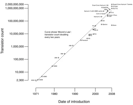
According to Moore’s Law, in the last 30 years the density of microelectronic devices in a chip has doubled every 18 months (Figure 1.1).
Thanks to Moore’s Law, for many years technological improvements were enough to obtain better performance, due to the the increase of frequency associated to the reduction of the size of transistors. Technological improvements were not the only way to go faster, as there was also an architectural development. The instruction
level parallelism (ILP) in the past has taken advantage of the incrementing
num-ber of circuits that was possible to put in a single chip. Successfull techniques as pipelining, superscalar processors, out-of-order execution, register renaming, specu-lative execution and VLIW architectures were largely adopted. At the same time, cache hierarchies have been used to mitigate the difference of speed between external memories and the processor (the Memory Wall [16]), that was becoming larger and larger. Both technological and architectural developments lead to the the improve-ments of computing power shown Figure 1.2.
In the past, parallelization an exception : to increase the performance of a pro-gram it was fairly more convenient to wait for a new faster processor than trying to parallelize the code. When the main concern was the throughput (in terms of number of task completed for unit of time), a solution was to adopt systems with
Figure 1.1: The trend of the density of microelectronic devices inside a chip in the last decades..
Figure 1.2: The improvements of computing power of processors in the last 30 years (This figure is Figure 1.1 in [17].
1.1. THE RAISE OF MULTI-CORES 3
multiple CPUs, to increase the number of tasks that could be processed concurrently. Nonetheless, in HPC parallelism has always been widely exploited. During the Eighties the HPC world was dominated by systems composed by few (four to sixteen) vector processors (although the first vector processors appeared in the Seventies) while the early Nineties saw the rise of Multiprocessors (MPP). However , until it was easy to get more performance with a single processor, data and processor parallelization was a concern only to specific fields, like high performance scientific programming.
Both technological and architectural developments were aimed to get a better performance with a single thread of execution, and both have now reached their limits, or it is too expensive to further develop them. As a consequence paralleliza-tion at each level seems the only viable way to continue to improve performance, as very little improvements in serial performance of general purpose processors are expected. To increase the performance of a processor has become harder and harder for several causes:
• the Power Wall • the Memory Wall • the ILP Wall
Physical limits of semiconductor-based microelectronics have become quite crit-ical under various aspects. Power dissipation is proportional to the clock frequency, and as a consequence there is a natural limit to clock speed. More precisely, power consumption typically rises as the square or cube of the frequency. With current cooling systems and material technology, a significative increment of frequency is not to be expected.
The increase of speed of processors was not matched by an equal increase of the speed of memory. As a consequence, due to latency and bandwidth, it is difficult to give the processor enough data to exploit its computational power. Usually this kind of problem is mitigated with the use a hierarchy of caches, but actually the cache occupies the higher fraction of a die and is responsible of a large amount of heat dissipation. So, the Memory Wall is also one of the major responsible of the huge power dissipation of modern processors.
The techniques for ILP exploitation are effective if the code is predictable and if enough instructions are submitted to the processor. Both code and data suffer from the Memory Wall bottleneck. Moreover, ILP require a super-linear increase of CPU complexity and associated heat dissipation without granting linear speedup.
To summarize, power consumption rises as the square of cube of the frequency, while the expected speedup is less than linear, so increasing the frequency is no longer convenient. A more aggressive exploitation of ILP would require more complex
hardware and as a consequence the power consumption is too heavy with respect to the to achievable benefits. Moreover, feeding the processor with data is difficult due to memory latency, that can be mitigated with caches, that also requires more circuits and improve heat dissipation.
Given that the increase of the frequency or complicated ILP logic are no longer a viable solution, possible solutions to obtain more performance are: production of smaller chips, increase the amount of cache, addition of more cores or improvement of memory bandwidth [18]. To balance these different options is not a trivial problem and each CPU developer is proposing its own solution. Generally, the number of cores have been incremented, and at the end of 2008 quad-core processors are the standard and architectures with more cores are also available.
Typically the clock speed increase has been stopped, and in many cases it is
slower than those of the last uni-core CPUs. Commodity processors also have
adopted power saving technologies that in the past was exclusive of mobile and embedded processor. Also the ILP hardware has been subject to minor refinements and in most cases has been heavily simplified or removed (as in CBE and GPUs). In general, there is more interest in data-level parallelism (the rise of SIMD ISAs) and, as long as there are more cores, it can be exploited at a higher level of abstraction. The memory wall is still a problem: memory is slowly becoming faster in terms of bandwidth but, as there are more processor to feed, the problem can be worse than before. Luckily, it is possible to put large on-chip caches that can help to mitigate this problem. However, as have been observed in [19, 18, 20, 21] this problem is expected to become worse and wors in next years, when there will be hundreds or thousands of cores inside a single chip.
Multi-core processors have to be appropriately programmed to guarantee per-formance improvements, and as a amtter of facts many applications have to be reengineered and restructured as parallel programs. First of all, all the available parallelism has to be exposed. Some applications are intrinsically parallel, while other are less likely to take advantage of concurrency. The critical point is the rele-vance of the parallelizable fractions of the program into respect of global execution time [22]. The availability of many computational resources cannot be exploited if an application is memory bound. In this case the bottleneck is represented by data transfer channels, between computational cores and main memory of between cores. From this point of view, multi-core processor have an interconnection infrastructure that is more efficient than those available in many multi-processor machines, so is more probable that computational resources can be efficiently used.
1.2. TOWARD MANY-CORES 5
1.2
Toward Many-Cores
It is expected that the number of cores inside a chip will double at each generation and that in few years processors with 128 or more cores will be available. Processor with hundreds or thousands of cores are classified as “many-core” [19]. Some special purpose processors have already tents of cores, like the Cisco QuantumFlow 40-cores newtwork processor (able to support up to 160 threads [23]) and, although this inter-pretation is ambiguous, GPUs have already hundreds of independent computational units.
Although many-cores do not still exists, it is possible to foresee that Memory Wall will be the primary concern [24, 25, 18, 26, 27]. As reported in [28], traditionally the CPU speed increases by 70 percent per year, while the bandwidth increases by 25 percent per year, and the memory latency shows the lowest improvement with a modest decrease of the 5 percent. With the actual “few-core” machine data access is a very important issues, and in many cases the computational resources are not used efficiently. It the next year will be very important to find new strategies to face the Memory Wall issue.
1.3
Multi-Core Architectures in 2008
At the end of 2008, multi-core architectures have become the standard. The two extremes of the spectrum are the commodity processors from Intel and AMD on one side, and the GPUs of NVIDIA and AMD (that has acquired ATI) on the other side. In the middle, there are processors like the Cell Broadband Engine and many other processors aimed at more specialized targets.
Commodity CPUs are largely based on the old single-core processor, which are replicated two of four times inside a single chip. A major feature is the presence of large shared caches between the cores, that are also connected by high-speed on-chip buses. The cores inside a processors are homogeneous and, although their ISA supports SIMD extensions, in principle they are multi-pourpose cores. While in HPC context it is vital to be able to use all the cores in parallel to gain a speed-up for a single program, theis chips are largely used as desktop or server processor, where multiple tasks are run in parallel, so distributing processes among the cores is sufficient to assure a performance gain.
At the other extreme, GPUs are based on arrays of simpler cores. Although the definition of “core” in this context is quite ambiguous, the amount of exploitable parallelism inside a GPU is much greater than those found in a multi-core CPU. To be used efficiently, a GPU has to run a program that has been subdivided into many subtasks. A basic concept of modern GPU is to run more threads than available cores, in order to mitigate the inevitable stalls intrinsic in each sub-task. To succeed in this purpose, in a GPU the context switch is very inexpensive. However, GPUs
are highly specialized for compute-intensive and highly parallel applications so, while they can deliver impressive performance in their specific area, they are not general purpose processors.
GPU are aimed at a fine-grain parallelism, as the single core is very simple and it is not flexible as a general pourpose processor. Multi-core CPU are instead oriented to coarse-grain parallelism, as a single core is capable to run complete applications (that it is not possible with the core of a GPU) and in some fields the presence of multiple cores is simply exploited to improve the throughput of the system, intended as the number of jobs completed for unit of time. At the other extreme, to obtain high performance in a GPU it is necessary to subdivide a single job into many threads that can are executed concurrently.
These two different philosophies are converging: in recent years specific-purpose extensions were added to general purpose processors, while GPUs are trying to become more general purpose in order to be used in scientific and multimedia pro-gramming, and not only in 3-D graphics.
CPUs and GPUs also differs from the point of view of memory hierarchies. While CPU are still based on caches to try to mitigate the Memory Wall, GPUs are based on customized an special pourpose on-chip memories. Moreover, GPUs usually have a dedicated Video RAM that is faster, although smaller and more expensive, than the memory used by general pourpose processor (for example the latest Intel CPUs can uses various GBytes of DDR3 memory with a bandwith of 32 GB/s, while the last NVIDIA GPU uses GDDR3 memory with a bandwidth of 141.7 GB/s, but it is limited to 4GB).
Both actual commodity CPUs and GPUs are homogeneous multi-cores, although GPU in the past were composed by two types of specialized cores (vertex and pixel shaders). Despite that, it is not obvious if homogeneous are better than heteroge-neous multi-cores.
A notable exception is the Cell Broadband Engine, that was designed to run the tasks of both a CPU and a GPU. As will be explained in details later, it has a general purpose core that runs the operating system and a set of eight specialized cores that are used for compute-intensive tasks. Originally the CBE was intended as the only computational core of PlayStation 3, although later a GPU was added. For many other aspects (the complexity of cores, the interconnection, the instruction set and so on) Cell Broadband Engine stands in an hypothetical middle line between CPUs and GPUs.
Another notable exception is the core used for Cray XD1 [29], that embeds an FPGA, although this is more a co-processor than a true additional core.
1.3. MULTI-CORE ARCHITECTURES IN 2008 7
1.3.1
Cell Broadband Engine
The Cell Broadband Engine (CBE) is the first implementation of the Cell Broad-band Engine Architecture (CBEA), developed by a collaboration of Sony Computer Entertainment, Toshiba, and IBM (usually referred as “STI”). CBE is a rare case of an heterogenous multi-core: a PowerPC (PPE) core and eight Synergistic Processor Elements (SPE) are embedded into the same die.
Development began in late 2000 and the first processor were widely available at the end of 2006, mainly as the PlayStation 3 processor. The CBEA has been initially designed for game consoles and high-definition multimedia device, but it has been extended to support a wider range of applications, like blade servers and High Performance Computing [30].
The 64-bit PowerPC core is a two-way simultaneous multithreaded Power ISA v.2.03 compliant core, and it is used to run the operating system and is primarily intended as a dispatcher of workloads to SPEs and for top-level control of applica-tions.
The Synergistic Processor Elements are the main source of computational power of the processor. Their instruction set is optimized for SIMD operations and at 3.2 GHz they have a theoretical peak performance of 25.6 Gflops. Each SPE can directly access a private high-performance memory of 256KB (Local Store) with a constant latency, and cannot directly use the main memory. Data transfers between local store and main memory are performed via DMA transfers.
The nine cores (one PPE and eight SPE) and the main memory are connected together with the Element Interconnect Bus (EIB). The EIB is composed by eight rings that allows parallel data transfers. Each ring provides a bandwidth of 25.6 GB/s. To allow simultaneous transfers each SPE has its own Memory Flow Con-troller (MFC), a device that can perform DMA transfers autonomously, so that the SPE can concurrently perform computations.
The project started with the main goal of obtaining a performance enhance-ment of two order of magnitudes in respect to current game systems (in 2001, the PlayStation 2 with its Emotion Engine processor), and to develop a processor well suited for multimedia an floating-point intensive applications. The main target of the new processor was clearly the PlayStation 3, but also Digital Entertainment Center (as such devices and game console tend to converge in the last years), mul-timedia devices in general, and finally High Performance Computing, because the high computational power required by modern 3-D games is not too far from that required by scientific application.
Usually, in the past, performance improvements were obtained with faster clock frequencies, wider superscalar architectures, deeper pipelines and caches. In 2001 it was clear that this path was paying diminishing returns. First of all, due to tech-nological limitations incrementing clock frequencies lead to power consumption and
dissipation problems. Moreover, as memory technology did not show comparable speed enhancement in the last years, increasing the performance of a single core leads to higher data access latency, that can make useless the speed enhancement of a single core. In effect, much of the bandwidth of a system can only be used speculatively, due to latency. Latency-hiding requires expensive and sophisticate hardware, and makes nearly impossible for the programmers to perform low-level optimizations.
The basic concepts that drove the development of the CBE where essentially to use powerful but simple computational cores and to connect all the elements of the system (including the memory) with a high-bandwidth interconnection bus. To allow an effective use of the available bandwith, simultaneous direct memory access can be performed without the assistance of computational cores.
More precisely, a general pourpose core (the PPE) is used to run the operating system an all the normal activities. Computational load is managed by multiple specialized cores (the SPEs), that are very fast and efficient for specific applications ( single-precision floating point intensive computations, with predictable branches) but are not suited for general applications. Independent entities (the MFCs) perform DMA data transfers, so that techniques as prefetching can be effectively used and the impact of the latency is hidden.
Notably, each SPE can directly use only its 256KB local memory, and data transfers between main and local memory have to be explicitly requested to the MFCs. SPE have not cache hierarchies and do not support out-of order execution. This simplifications allowed to multiply easily the number of cores embedded into a single die.
Power Processor Element
PPE is a dual-issue, in order implementation of the IBM PowerPC Architecture, with vector multimedia extensions (VMX). It includes a 32KB L1 cache for both data and instructions and a 512KB L2 cache. The register file is composed by 32 x 64-bit general pourpose registers and 32 x 64-bit floating point registers. Moreover, there are 32 VMX 128-bit registers. The PPE is able to interleave instructions from two separated hardware threads. This means that state register are duplicated, but functional units, caches and queues are shared. The pipeline depth is 23 stages, considerably less than the previous implementation of PowerPC processors. Inte-ger arithmetic and load instructions complete in two cycles, while double-precision floating-point instruction requires ten cycles. [30] Although the primary target of PPE is not computation, VMX extension allow a peak performance of 25.6 Gflops in single-precision when running at 3.2 GHz.
The PPE has not an associated MFC, so to perform DMA transfers it has to remotely access the MFC of the SPE involved in the data transfer.
1.3. MULTI-CORE ARCHITECTURES IN 2008 9
One of the major benefits of PPE is its backward compatibilyty with the Pow-erPC software. In this way it was not needed to write the operating systems and the toolchain from scratch, thus shortening the development of the processor and allowing the CBE to run existing software once it was ready.
Synergistic Processor Element
A Synergistic Processor Element (SPE) contains a Synergistic Processor Unit (SPU) and a Memory Flow Controller (MFC). The SPU is composed by the 256KB Local Store and the SIMD functional units. The MFC is a DMA controller with a MMU (to help address translations) and an atomic unit (to allow synchronizations). The SPU and the MFC operate concurrently and independently.
As said earlier, a SPU does not need to run the operating system, so it does not support mechanisms like address translation and protection (that are delegated to the MFC). A SPU can operate only on data and instructions memorized into the local store. It can communicate with the other elements of the system (including main memory) only via DMA transfers performed by its own MFC or by one of the other MFCs. A SPU sumbits DMA transfer requests to MFC through a channel interface.
The instruction set of the SPEs is not the same of that of the PPE, although it is quite similar to VMX extensions. In any case, binaries are not compatible. In particular, the SPE ISA has specific instructions to issue commands to the MFC.
A SPU is essentially a SIMD architecture and it is organized around a 128bit dataflow. It has a large unified register file composed by 128 SIMD registers 128-bit wide, that allows deep unrolling to cover functional units latencies. It does not supports out-of-order execution nor branch prediction but, because the local store has a constant latency, its behavior is predictable and optimizations can be performed at compile time.
A SPU supports various levels of SIMD-granularities:
• 16 × 8-bit integers (bytes) • 8 × 16-bit integers (half-words) • 4 × 32-bit integers (words) • 2 × 32-bit single-precision floats
Each SPU has two separate pipelines, so it’s able to issue two SIMD instruc-tions for each clock cycle if they are of different types. The “even” pipeline is able to perform float and integer computation, while the “odd” pipeline is dedicated to loads, store, branches and other operations that involve bits manipulations. A
Figure 1.3: The SIMD-granularities supported by CBE. Note that each type of instructions sup-ports only specific types of variables. For example, single-precision floating-point instructions supports only the “word” (four 32-bit scalar variables) granularity. (Figure is from [31])
somple but very important implication is that load/stores instructions can in prin-ciple be executed in parallel with computation, thus allowing a higher efficiency in single-precision floating-point pipeline exploitation. Single-precision floating-point instructions are executed in 6 cycles, while integer and logic instructions are per-formed in only two cycles. In the first release double precision instructions are not pipelined and require 7 cycles. When using single-precision floating point, if a multiply-add is issued at each clock cycle, at 3.2GHz a peak performance of 25.6 Gflops can be achieved.
The register file has six 128-bit read-only and two 128-bit write only ports, that are enough two feed two instruction that takes each one four operand (a multiply-add in the even pipe and a shuffle in the odd pipe, for example). A 128-bit bidirectional port connects the register file to the local store. A load/store instruction has a fixed latency of six clock cycles. As said earlier, the fixed latency allows various optimizations, but in principle local store access can be a bottleneck. However, the size of the register files allows to store a large amount of variables, thus reducing the local store access. Local store has also a 128-bytes read-only port used for instruction fetching an to send data to the MFC and a 128-bytes write-only port to get data from the MFC. However, the EIB can take only 8 bytes for cycle (which means 25.5 GB/s for each direction), and in this way the local store can be accessed only once every 8 cycles.
Unlike traditional processors, a SPE is not a scalar core with SIMD extension, but is completely SIMD. Scalar programs simply use a single slot of the SIMD registers. A SPE support only a single program context at any time. A context can be a user application (“problem-state”) or operating system extension (“super-visor”). Moreover, a “hypervisor” state allows multiple operating systems to run concurrently.
1.3. MULTI-CORE ARCHITECTURES IN 2008 11
We have said that the MFCs move data across the system. In particular, there are three different types of information exchange: signals, mails and regular DMA transfers. Signals and mails are 32-bit messages that are stored in special-pourpose queues, while regular DMA transfers are transfers take play between main and local memory or between two local memories, and can range from 1 byte to 16 KBytes. Although signals and mails are actually implemented as DMA transfers, in future CBEA compliant processors they will have a dedicated data-path.
Element Interconnect Bus
The Element Interconnect Bus (EIB) consists of one address bus and four 16-bye data rings, two of of them running clockwise and the other two counter-clockwise. Each ring support up to three concurrent transfers if the paths do not overlap. The EIB operates at half the speed of the cores, so at the reference clock speed of 3.2
GHz it can sustain a bandwidth B0 of
B0 = 3× 4 rings × 16 bytes × 1.6 GHz = 307.2 GB/s (1.1) Each element connected to the EIB can send and receive 16 bytes of data every bus cycle, so the bandwidth at which each element can send or receive data is 25.6 GB/s in both direction, for a total bandwidth of 51.2 GB/s.
The maximum bandwidth of the EIB is limited by the address snooping. Only one 16 byte long data transfer can be snooped per bus cycle. Each snooped address request can potentially transfer up to 128 bytes, so the theoretical peek is:
B = 128 bytes × 1.6 GHz = 204.8 GB/s (1.2) To send data to another unit, each element makes a request to the data ring arbiter on the the EIB. The arbiter decides which ring is granted and to which requester in which time slot, trying to optimize the EIB usage. The higher priority is given to the memory controller, because memory is a precious shared resource. All other elements are treated with a round-robin priority.
Any requester can use any of the four rings, given that it does not interfere with another transfer already in progress. Moreover, a ring is not assigned to a requester if the transfer would cross more than halfway around the ring on its way to destination.
Sustained bandwidth can be lower than the peak bandwidth because of several factors: the relative positions of the sender and of the receiver (for example, a six hops transfer inhibits the unit on the way to use the ring), the number of requests to the same destination and the number of requests per direction. Moreover, the bus efficiency is lowered when there are a large number of partial cache line transfers.
The EIB is coherent to allow a single address space shared by all the elements connected to the bus.
Memory
The internal memory controller (MIC) of the first implementation of CBE is con-nected to the external Rambus XDR DRAM through two XDR controller I/O (XIO) at 3.2 GHz. Each channel can support eight banks, for a maximum size of 512 MB. The MIC manages independently the read and write requests queues for each channel. Writes in the range 16-128 bytes can be directly written to memory using a masked-write operation, while writes less than 16 bytes require a read-modify-write operation. The peak raw memory bandwidth is 25.6 GB/s, although management operations reduce it to 24.6 GB/s when all requests are of the same type. If reads and writes are intermingled, the effective bandwidth is reduced to 21 GB/s, due to the need to turning around the MIC-to-XIO bus.
The PowerXCell 8i implementation supports DDR2 memory instead of XDR DRAM, supporting up to 32GB of memory with ECC and a bandwidth of 25.6 GB/s.
Flexible I/O Interface
The CBE has seven transmit and five receive 5GHz, byte-wide Rambus FlexIO links, that are configured as two logical interfaces. When two processor are connected together, data and commands are transmitted as packets using a coherent protocol called “broadband interface” (BIF). BIF Operates over IOIF0.Typically the two FlexIO links are configured is such a way that an IOF0 has 30GB/s outbound and 20 GB/s inbound bandwiths and IOF1 has 5 GB/s outbound and 5 GB/s inbound and works in noncoherent mode. [32, 33] However, the flexibility of FlexIO allows to support different system configurations, from a single-chip configuration with dual I/O interfaces to a dual-processor configuration that does not require any extra chip to connect the processors.
Addressing
A peculiarity of CBEA is the definition of a main and a local storage domains [34]. The main one contains the address space for main memory and memory-mapped I/O registers and devices and is common to all the system. Each SPE has its own local domain that refers to its local store, used for both data and instructions. Each local domain is also mapped in main storage domain, in an address range called
local storage alias.
The instructions that compose a CBE program use the effective-address space, while the processor itself supports the real-address space. A combination of hardware and operating system support allows to also support a virtual-address (VA) space. Both PPE and MFCs have dedicated hardware for address translation. The Cell
1.3. MULTI-CORE ARCHITECTURES IN 2008 13
Figure 1.4: Block diagram of the CBE processor. Figure is from [32].
Broadband Engine Architecture (CBEA) processors is compatible with the PowerPc virtual-storage environment that is compatible with that defined by [35].
The real-address (RA) space is the set of all addressable bytes in physical memory and on devices whose physical addresses have been mapped to the RA space (as the SPEs local stores and MMIO registers).
The PPE uses effective-address (EA) address. Each SPE can access the EA space through MFCs and use local-storage (LS) addresses to access its own local store. Each MFC command has a pair of EA and LS addresses.
Virtual-address translation can be activated independently for instructions and
data. Each PPE program can access 264 bytes of EA space, that are a subset of 265
bytes of virtual-address (VA) space. A EA address is translated into a VA address,
and then in to a RA address. RA space is composed by 242 bytes. An overview of
address translation is shown in figure 1.5.
VA space is subdivided in protected and nonoverlapping segments of 256MB of contiguous address, while RA space is subdivided in protected and nonoverlapping
pages that contain a number of consecutive address between 4KB and 16MB.
The conversion from EA to RA is performed in two steps: firstly, the EA is converted to VA using the SLB (segmentation) and then the VA is converted to RA using the page table (pagination).
The virtual-address mechanism allow to associate different restriction and dif-ferent attributes (like cacheability and coherence) to each page or segment.
Figure 1.5: PPE Address-Translation Overview. Figure is from [36].
In general CBE architecture makes all SPE resource available through MMIO. There are three main classes of resources:
• Local Storage. The local stores of all SPEs. PPE can access to SPU’s local
storages using load and stores, but this process is fairly inefficient and is not synchronized with SPU execution
• Problem State Memory Map. These resources are intended for use by the
ap-plication and includes MFC MMIO, mailbox channels and signals notification channels
• Privilege 1 Memory Map. Resources for monitoring and control by the
oper-ating system of the execution of SPU programs
• Privilege 2 Memory Map. Resources for control of SPE by operating system
The local store of each SPE is mapped into main memory, for programming convenience, but they are not coherent in the system. Figure 1.6 shows an overview of the mapping of SPEs resources into effective address space.
MFC and DMA Transfers
DMA requests can be issued to MFC in various ways. The SPU of the same SPE can use specific instructions to insert commands in the queues, or it can prepare a
1.3. MULTI-CORE ARCHITECTURES IN 2008 15
Figure 1.6: An overview of the mapping of SPEs resources into effective address space. Figure is from [36].
list of commands in the local store and issue a single “DMA list” command to the MFC. These commands are issued using the channel interface.
Channels are unidirectional communication paths that work like fixed-size FIFO queues. Each channel is either read-only or write-only, and can be blocking or non-blocking. Each channel has an associated count that indicates the number of elements in the queue. Three instructions allow the SPU to interact with the channel interface: read channel (rdch), write channel (wrch) and read channel count (rchcnt). The CBEA specifies the depth of some channels, while for the others it is an implementation specific parameter (for further details see [37]).
All other elements connected to the EIB can insert commands in specific “proxy” queues using memory-mapped (MMIO) registers (see section 1.3.1).
Each MFC processes two separate DMA command queues:
• MFC SPU command queue, that contains the command issued by the local
SPU
• MFC proxy command queue, for the commands issued using MMIO registers
by other elements connected to the EIB
The CBE architecture does not specify the size of the queues, but when they are full the result is a performance degradation, as the core issuing commands stalls until the queue is free. Alternatively, non blocking instruction are available to access the queues. In the first implementation, the CBE, the MFC SPU queue contains 16 entries and the MFC proxy command queue eight entries.
A single DMA command can request the transfer of 1,2,4 or 8 bytes or a multiple of 16 bytes, up to 16KB. A DMA command list, that is accepted only by MFC SPU queue, can request up to 2048 DMA transfers. A DMA list is an array of source/destination address and length tuples that is stored in the local memory. Both source and destination addresses have to be 16 byte aligned. The hardware can transfer only 128-byte aligned blocks of 128 bytes, so the peak performance is achievable only if both addresses are 128-byte aligned and the length of the transfer is a multiple of 128 bytes.
The MFC supports also two signaling channels. The SPU access the channels using the channel interface, while the PPE has to use the MMIO registers. It is possible to perfrom a logical OR of the signals of all the SPU of the system.
Each MFC has also three 32-bit mailbox queues: a four-entry, read-blocking inbound mailbox and two single-entry, write-blocking outbound mailboxes. One of the outbound mailboxes is able to generate interrupts to PPE when it is written by the SPU. The PPE has to use MMIO registers to write the SPUs inbound mailboxes or to read from SPUs outbound mailboxes. Mailboxes are well suited for one-to-one communications, and the roundtrip time between two SPUs is approximately 300 ns ([33], or 960 clock cycles (at 3.2 GHz).
1.3. MULTI-CORE ARCHITECTURES IN 2008 17 PowerXcell i8
PowerXcell i8 is based on a 65nm process and the main difference with is prede-cessor is the support of DDR2 memory and better performance for double-precision floating-point operation.
DDR2 memory has been chosen because it allows the use of a greater amount of memory per board. CBE was limited to 1GB per board, clearly insufficient for HPC applications. Now a single processor supports up to 4 DIMM slots and up to 16GB of memory.
The peak bandwidth has been preserved by expanding the memory buses to 128-bit, although this implies an increase of pin count and pin incompatibility with previous generations.
While in the first implementation of CBE double-precision floating-point perfor-mance where fairly poor, now a single SPE is capable of 12.8 Gflops, which lead to a peak performance of the whole processor of 102.4 Gflops [38].
While double-precision functional units are fully IEEE 754 compatible, single-precision is not fully compliant due to truncations.
The next generation of CBE processor should be released in 2010. The number of SPE should be expand to 16 or 32 using a 45nm process [38].
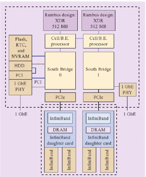
CBE blades
In IBM QS211 blades, two CBEs are configured as a two-way, symmetric multipro-cessor (SMP). Each promultipro-cessor has its own directly connected Rambus XDR memory and it is connected to a separate South Bridge.
The bandwidth of the interface between the CBE processor is 20 GB/s in each direction, and it is realized through FlexIO.
The bandwidth of the South Bridge interface is (CIRCA) 1.0 GB/s in each direction. The South Bridge 0 chip provide all the required features: a PCI-E channel, a PCI bus interface, an IDE channel, a Gigabit Ethernet interface, USB 2.0 ports, a UART and an external bus controller. More details can be found in [39].
An interesting feature of the dual-processor configuration is the possibility to perform DMA transfers between the local stores of the SPEs belonging to different processors. Moreover, a SPE can access both memories, although accessing the local memory is faster.
QS22 is an updated version of QS21 with PowerXcell 8i processors and DDR2 memory. In each board there are two 3.2 GHz PowerXcell 8i connected via BIF interface. Each processor can be equipped with up to 16GB of DDR2 memory.
Figure 1.7: The organization of a QS21 Blade Server. Note that the two processors are directly connected and that, although some resources are shared (as the PCI interface), each processor has its own XDR memory, Gbit PHY and PCIe interfaces. Figure is from [39].
1.3. MULTI-CORE ARCHITECTURES IN 2008 19
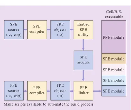
Figure 1.8: The compile chain of CBE. Note that the executable of PPE and SPEs are compiled independently, and that only in the linker phase are united into a single executable file. Figure is from [39].
Application Development
The Cell Broadband Engine is supported by Linux, and the Cell Broadband Engine
(Cell/B.E.) Software Development Kit (SDK) provides all the tools needed to
de-velop an application for CBE. The two main alternative are the GNU Toolchain or the IBM XLC/C++ compiler, although Fortran and ADA compilers are also available.
The SDK include various libraries, including the SPE Runtime Management Library that allow to run executables on the SPEs.
The CBE is an heterogeneous processor that supports two different instruction sets. Two distinct toolchains are used for the two types of core, although both toolchains produce executables in ELF format. An interesting feature is the CBE
Embedded SPE Object Format (CESOF), an application of the ELF of the PPE that
allows PPE executable objects to contain SPE executables [36, 40].
CBE Programming
The issue of efficiently programming the CBE has been widely analyzed in literature. OpenMP [41] and MPI [42] have been ported to CBE, so it is possible to port old programs with a relatively small effort (although efficiency is not guarantee) and it is possible to continue to adopt these two well-known programming paradigms.
As long as data-transfers and local memories usage is completely software con-trolled, it is important to understand which is the best way to manage them [43]. There are also many researches in the field of compilers and automatic code gener-ation [44, 45, 46, 47, 48], as CBE processor in-order hardware requires a non trivial programming effort to produce optimized code. Many scientific application have already been ported to CBE [49, 50, 51, 43, 52, 53, 54, 55, 56, 57, 58].
1.3.2
Intel Nehalem
Nehalem is the first Intel “real” quad-core processor and it is availabel since Novem-ber 2008. In a single die are embedded four cores. Each core has 32 KBytes of L1 program cache and 32 KBytes of L1 data cache. Each core has also its own 256 KBytes L2 cache. The four cores also share 8MB of L3 cache. L3 cache is inclusive: if a line is in L1 or L2, then it’s also in L3. This prevents the need to snoop L1 and L2 of each core. The die also integrates the memory controller. Nehalem supports DDR3 RAM with a bandwidth of 32 GB/s. In multiprocessor configurations, CPUs are connected through the Quick Path Interconnect, that provides a bandwidth of 25.6 GB/s in both directions.
Each core supports hyper-threading and SSE4.2. It has also 4-wide dynamic execution engine and has hardware dedicated to loop detection.
1.3.3
AMD Shangai and Istanbul
Shangai chips are the first AMD’s 45 nm processors and features 4 cores in a single die. Three level of cache are present: 6 MBytes of L3cache are shared between the cores, while each core has 512 KBytes of L2 cache and 64 KBytes of L1 data and instruction cache.
DDR2 RAM is supported at up to 800MHz, while DDR3 RAM is not supported. Only HyperTransport 2.0 (with a bandwidth of 8 GB/s) communication bus is supported.
Shangai processors supports SSE and SSE3 SIMD instructions, and add the support to AMD’s SSE4a, that are incompatible with Intel’s SSE4.1
In the second half of 2009 Istanbul processors will be available. They will feature 6 cores and will add the support for DDR3 RAM and HyperTransport 3.0 commu-nication bus, with a bandwidth of 17 GB/s. The cache hierarchy will be unchanged, and the die size will be of 300mm.
1.3.4
NVIDIA GT200
At the end of 2008 NVIDIA high-end GPU offer is the GT200 Series, that are used across the GeForce, Tesla and Quadro product lines.
1.3. MULTI-CORE ARCHITECTURES IN 2008 21
As long as we are interested in computational peak performance, CUDA pro-gramming model and implications will not be discussed.
A GT200 GPU is structured wtih many levels of hierarchy and a direct com-parison with “standard” multi-core architectures is not always possible. A GT200 GPU is composed of 10 Thread Processing Clusters (TPC), each of one is made of 3 Streaming Multiprocessors (SM) and one memory pipeline. Each SM is composed by 8 Streaming Processors (SP). An SP has a private program counter and a set of registers, but it is not an independent core, as it lacks may features, like a fetch unit, and it is equivalent to a scalar 32bit pipeline in a multi-threaded CPU.
The Streaming Multiprocessor is the smallest independent unit of the GPU, and its similar to a single-issue processor with 8-way SIMD support.
NVIDIA defines its computational model as Single Instruction, Multiple Thread (SIMT). The main difference with SIMD is that while SIMD exposes architectural width and data must be packed into vectors and the same operations are applied to all the scalars packed into a vector, in SIMT each thread works on it’s own data and it’s possible for each thread to take independent branches (with a loss of performance if the threads diverges).
Each SM has 64 KBytes register file (16 KBytes × 32bit) partitioned between
SPs, and a 16 KBytes shared memory with the same latency of the register file for communication between threads. Data cannot be directly loaded from main to shared memory. Data can be exchanged between the main memory and the register file and between the shared memory and the register file, so a transfer between shared and main memory requires an intermediate step into register file.
Each SM has a shared fetch unit and a set of eight 32bit ALU that can perform a multiply-add between IEEE single-precision floating point in 4 clock cycles. More-over, each SM includes a double-precision execution unit and a Special Function Unit (SFU) for reciprocal, interpolation and other special functions. The SFU can also be used to perform two extra 32bit madd.
Load/Store units are decoupled from the computational units. Each Thread Processing Cluster (TPC), as said earlier, has three SMs and a texture pipeline
that is used to access the render output (ROP) units. Load/store instructions
are generated by SMs, but they are issued and executed by the texture pipeline. The texture pipeline has two texture caches that, unlikely traditional caches, have 3-dimensional locality. Moreover, they are read-only and have no cache-coherency. Texture caches are intended to save bandwith and power, and do not impact latency. Each TCP embed 24 KBytes (8 KB for each SM) L1 caches, while a 32KB L2 cache resides with the memory controller.
Main memory load/stores must be 4 bytes aligned. Load instructions of different threads can be coalesced to reduce the total amount of transactions.
A GT200 chip requires 1.4 billions of transistors and is fabricated with 65nm
• graphics clock, used for texture pipeline, ROPs and SM (except SP functional
units)
• processor clock, the double of graphics clock, used for SPs • memory clock, used for the GDDR3 memory controller
Typically the processor frequency is 1296MHz, while memory frequency is 1107MHz. The peak performance is 933.1 Gflops in single precision and 77.8 Gflops in double precision. The GT200 supports GDDR3 memory that allows a bandwidth
of 141.7GB/s. Typically 1GB is mounted on each board, but up to 64GB are
supported. The TDP 1 is of 236W under load, but it goes down to 25W when idle.
1.3.5
AMD ATI RV770
At the end of 2008 AMD high-end is represented by the RV700 GPU. An RV700 contains 10 SIMD cores. Each SIMD core is composed by 80 Stream Processors Units grouped into 16 Stream Processors. A stream processor can execute up to 5 instructions in parallel if they belong to the same thread. Each SIMD core has also 4 Texture Address Units (TAU), 16KB L1 cache and 16KB of Global Data Share memory. L1 cache bandwidth is 480 GB/s
In the chip are embedded 4 x 64bit memory controllers, that also integrate a L2 cache. The bandwith of transfers between L1 and L2 cache is 384 GB/s. Memory controllers supports GDRR3/4/5. Hi-end boards mount 1GB of 900MHz GDRR5, for a total bandwidth of 115.2 GB/s.
RV770 contains a PCI-e 2.0 bridge that allows a bandwidth of 10 GB/s for both communications with the main memory and a second GPU in multi-chip configura-tion. Moreover, two RV770 are also connected with a Sideport bus that allows an extra bandwidth of 10.2 GB/s.
The die size is 256mm2 and there are 956M transistors. The TDP is 250 W.
In high end configuration the clock speed is 750 Mhz. If all Stream Processor Unit are concurrently performing a multiply-add, its possible to achieve a single-precision floating-point peak performance of 1.2 Tflops with a single GPU. Double-precision performance is 240 Gflops.
1.3.6
Many-core: Intel Larrabee
Intel Larrabee is a project for a discrete GPU based on x86 cores. Presumably it will be available at the end of 2009. The basic idea is to embed 32 or more cores into a single die. While NVIDIA and ATI GPU are based on programmable but
1TDP is the Thermal Design Power and represents the maximum amount of power the cooling
1.4. CONCLUSIONS 23
highly-specialized cores (stream processors), Larrabee will have very little graphic specialized hardware, and each core supports the well-know x86 ISA, with the ad-dition of a 512bit vector processor unit that can perform the same operation onto 16 independent floating point variables. The consequence is that Larrabee should be more flexible than a traditional discrete GPU.
Concerning data model, while a traditional GPU highly-specialized memory, Larrabee supports cache coherence between cores and it provides instructions for cache manipulation. The cores are interconnected with a 1024-bit wide interconnect bus.
1.4
Conclusions
Table 1.1 shows a comparison between the multi-core architectures available at the beginning of 2009.
GPUs are very impressive, as they feature the highest number of cores (they are the first example of many-core architectures), although they are designed for a narrow range of applications. Howeverer, today there is a great interesting in the General Purpose GPU programming (GPGPU). Both NVIDIA and AMD are try-ing to introduce GPUs into to the world of high performance computtry-ing, propostry-ing two software infrastructures that allow to use GPUs for general purpose computa-tion (NVIDIA CUDA [59] and AMD ATI [60]). The OpenCL (Open Computing Language) framework has been proposed as a effective way to write programs that executes across heterogeneous platforms as CPUs and GPUs.
Multi-core processors are more general purpose than GPUs, but they also suffer from the relatively small bandwidth of main memory. Moreover, the relatively small number of cores now available does not allow to fully take advantage of parallelism. However, the future trend should for commodity processors should see a doubling of the number of cores every 18 months, so that in 2015 general purpose many-cores processor with 1024 cores should be available. For that time, it is not clear which amount of parallelism will be achieved by GPUS, and if CPUs and GPUs will have converged into a single type of device. In the next few years the first chips including both CPU and GPU in a single die are expected.
The CBE processor seems to take advantage from the best of the two world, because it has more cores than a commodity processor and, although they are not well suited for every type of applications, they are more general purpose than the streaming processors included in GPUs. Moreover, the presence of on-chip memory completely under software control should allow to refine compiler technology in order to be able to automatically adapt the programs to the available resources. However, the balance of computational power and data transfer channels is algorithm dependent, so while CBE grant high computational power in some application, each
CBE PowerXcell i8 Nehalem Shangai GT200 RV770 Cores 1+8 1+8 4 4 10 10 32bit-ways x core 4 4 4 4 24 80 32bit-ways x chip 32 32 16 16 240 800 SP Fops x chip 64 64 16 16 720 800 Clock (GHz) 3.2 3.2 3.2 2.7 1.3 1.5 Peak SP Gflops 230.4 230.4 51.2 43.2 933.1 1200 Peak DP Gflops 13+20 13+100 77.8 240 Process (nm) 90 65 45 45 65 55 Transistors (M) 241 250 731 758 1400 956 Die size (mm2) 235 212 246 243 583.2 256 TDP (W) 80 100 130 95 236 250 Memory XDR DDR2 DDR3 DDR2 GDDR3 GDDR5 Memory BW (GB/s) 25.6 25.6 32 25.6 141.7 115.2 L1 cache x core 256KB 256KB 32KB+32KB 128KB 24KB L2 cache - - 4 x 256KB 4 x 512KB 256KB L3 - - 8MB 6MB
-IEEE SP no yes yes yes yes no IEEE DP no yes yes yes yes no Speculative no no yes yes no no Model SIMD SIMD SIMD SIMD SIMT
Table 1.1: A comparison of the main multi-core architectures available at the beginning if 2009. The highest computational power are achieved by AMD ATI RV770 and NVIDIA GT200 GPU architectures, although an high efficiency can be achieved only in specific applications. Note also that the power dissipation of these devices is very high (at least the double of a processor) and that they use very fast memories. Typically a graphic board has at most 1GB of memory, that it is sufficient for video applications but much less than the amount of memory supported by a traditional processors. Intel Nehalem and AMD Shanghai architectures have both four cores and comparable amounts of on-chip memories. The cores of these devices are general-purpose processor, that grant an high flexibility but that also are an order of magnitude slower than GPUs in single-precision floating-point computations. Finally, CBE processors not only have 9 cores instead of 4, but also have a peak floating-point performance that is four times higher than those of Intel and AMD processors, although the computational cores are efficient only in computing-intensive applications.
![Figure 1.4: Block diagram of the CBE processor. Figure is from [32].](https://thumb-eu.123doks.com/thumbv2/123dokorg/4717860.45531/25.892.194.816.169.569/figure-block-diagram-cbe-processor-figure.webp)
![Figure 1.6: An overview of the mapping of SPEs resources into effective address space. Figure is from [36].](https://thumb-eu.123doks.com/thumbv2/123dokorg/4717860.45531/27.892.249.742.309.924/figure-overview-mapping-spes-resources-effective-address-figure.webp)