Hybrid photonic-plasmonic platform for
high-throughput single-molecule studies
M
INAM
OSSAYEBI,
1A
LBERTOP
ARINI,
2A
MANDAJ. W
RIGHT,
1M
IKEG.
S
OMEKH,
1,3G
AETANOB
ELLANCA,
2ANDE
RICC. L
ARKINS1,*1Department of Electrical and Electronic Engineering, University of Nottingham, Nottingham, NG7 2RD, UK
2Department of Engineering, University of Ferrara, Ferrara, 44121, Italy
3Nanophotonics Research Centre, Shenzhen University, Shenzhen, PRC, 518060, China *[email protected]
Abstract: We present the design and numerical characterization of a hybrid
photonic-plasmonic nanoresonator comprised of a 2D photonic crystal (PhC) cavity, a gold bowtie nanoantenna (BNA) and a silicon dioxide, SiO2, spacer. This device is designed to serve as
the building block of a multicomponent platform capable of running multiple single-molecule experiments such as optical trapping and sample interrogation simultaneously. The thickness and structure of the spacer layer are adjusted to maximize the energy in the externally accessible hot-spot in the BNA gap. Suitability of the device for photonic integration is demonstrated by exciting it through a PhC waveguide.
Published by The Optical Society under the terms of the Creative Commons Attribution 4.0 License. Further distribution of this work must maintain attribution to the author(s) and the published article’s title, journal citation, and DOI.
1. Introduction
In biophotonics, there has been a drive over the last few decades to develop high-throughput, single cell/molecule techniques that avoid the pitfalls of bulk-averaged measurements. Optical techniques, such as trapping, manipulation, sensing and spectroscopy have received considerable attention, since they are minimally-invasive, often label-free and have the potential to be reconfigured in real time giving flexible positional control of the cell or molecule of interest [1]. Whilst techniques such as optical trapping are single-cell, they are not high-throughput and often require lengthy experiments on many individual cells before reliable conclusions can be reached [2]. These techniques typically operate on the micrometer scale. There is also a need to push them to the nanometer scale to make single molecule experiments possible. Finally, integrated solutions are needed to remove the barriers to the clinical uptake of single-cell/molecule technologies created by the need for highly trained users, long repetitive measurements and large, high-cost optical systems.
Photonic integrated circuits with hybrid photonic-plasmonic nanocavites are a promising new technology for future high-throughput single-molecule experiments. Devices for these applications require externally accessible regions of high optical power densities and low power dissipation translating into a need for optical cavities with a high-energy storage capacity and strong external spatial localization. The energy efficiency or resonant enhancement of the energy storage capacity of the optical cavity is described by the quality
factor, Q 2 energy stored
energy lost per cycle π
= . The effective mode volume, Veff, described by
Kristensen et al. [3] is a commonly used measure of spatial energy localization. While Veff is a
well-established figure of merit for simple resonators, it can give anomalous values of mode volume for complex resonators where, for example, the confined light is coupled to a smaller externally accessible hot-spot. The challenge is to design a resonator with both a high Q and an externally accessible, nanoscale hot-spot for optical trapping and interrogation of single
#356672 https://doi.org/10.1364/OME.9.002511
Journal © 2019 Received 7 Jan 2019; accepted 11 Feb 2019; published 7 May 2019 Journal © 2019
molecules. This is driving the development of a new breed of hybrid photonic-plasmonic nanocavities and for this a different figure of merit will be introduced,
Plasmonic nanoantennas are able to localize light in regions a few tens of nanometers across, an order of magnitude smaller than the diffraction limit (~ 0.6
eff n
λ ), where λ is
wavelength of light and neff is the effective refractive index [4]. However, plasmonic devices
usually suffer from low resonant energy enhancement (Q < 100) due to radiation and absorption losses in the metal. Bowtie nanoantennas (BNAs) formed by placing two nanosized metallic triangles together with a narrow gap have been used in plasmonic nanotweezers [5–7], spectroscopy [8] and biosensing [9]. Nanoapertures in metal films have also been used for surface induced back action optical trapping of nanoparticles [10] and the trapping and unfolding of single proteins [11].
Photonic crystal (PhC) cavities, on the other hand, are extremely energy efficient and can achieve very high resonant enhancements (Q > 100,000) [12], but their spatial localization is limited by diffraction, with Veff of the order of the cubic wavelength. Unfortunately, the very
high intensity light in PhC structures is either confined within the dielectric material or in the holes or gaps in the dielectric structure. Thus, the hot-spots are either inaccessible for optical trapping or draw particles onto or inside the structure where they can adhere to the surface and become stuck.
This work designs a hybrid photonic-plasmonic resonator with both a high Q and an externally accessible, nanoscale optical hot-spot. This hybrid resonator represents a key building block that can be replicated many times to produce a multicomponent platform for high-throughput single-molecule experiments. This hybrid resonator is formed by combining a 2D PhC cavity, to provide an energy reservoir, with a BNA, to create an externally accessible nanoscale hot-spot. A dielectric spacer is placed between the PhC cavity and the BNA. The thickness and structure of the spacer controls the balance between Q of the cavity and the intensity in the external hot-spot. The resonant wavelength of these devices can be individually tuned by small changes to the PhC cavity. The inclusion of a PhC waveguide allows both fiber-optic coupling and the integration of hybrid resonator arrays for parallel trapping and interrogation. For arrays, the 2D photonic bandgap suppresses optical cross-talk between nearby devices.
This device builds on previous work combining PhC and plasmonic structures [13–38]. For example, C. Ciminelli, et al. (2014) designed and simulated a hybrid device based on a 1D PhC cavity coupled to a BNA [39]. They used a spacer block directly underneath the BNA, which hence only covered a small area of the 1D PhC. This device achieved high localization of light, but had a highly structured surface with etched features and holes, which may affect its future experimental performance. In our proposed device, the spacer layer covers the entire top surface of the device, not only the area underneath the BNA. The flat surface and compatibility with fiber optics make it practical for use in the life science applications.
2. The proposed hybrid device
The PhC cavity is based on a 275 nm thick gallium arsenide (GaAs) slab with a triangular lattice of air holes with periodicity, a = 410 nm, to form an air-suspended PhC membrane. An L3 cavity is formed by removing three adjacent holes from the PhC structure. The holes at the ends of the cavity are shifted by 0.2a outwards to increase the Q of the cavity [40]. GaAs was chosen due to its high refractive index resulting in high confinement of light in the vertical direction, but silicon and indium phosphide are also suitable. The L3 cavity is designed to operate in the 1530 - 1565 nm wavelength range to take advantage of well-established telecom technologies (e.g. photonic integrated circuits tunable lasers, fiber-optic components and test equipment).
The gold with a gap of procedures. T nm, also resu with a thickne the flow of en be extended leakage in thi cavity and or maximum of t The devic it well suited along the x d waveguide to Q of the hybri Fig. 1 gold B waveg 3. Simulatio The results pr on the 3D fin matched laye propagation in gold was rep [45,46]. A co interfaces of respect to the and mesh ac wavelength ( simulations. T Gaussian puls In order to ca the electroma points while slope of the performed as normalized to BNA consists f 30 nm (the di The tip full-ang lting in a reson ess, d, separate nergy between through the sp is layer. The B riented along th the fundament e can be effici for integration direction as sh
the cavity can id resonator, as
. (a) Illustration o BNA (yellow) and guide used to excit on method resented in thi nite difference r (PML) was n an infinite fr presented by J onformal mesh different diele number of PM ccuracy. A cha less than 1 n To study the r se was used as apture the mod agnetic field c the simulation decaying fiel s described in o the maximum s of two 40 nm istance betwee gle of each trian
nance in the 15 es the PhC from the PhC cavity pacer layer to NA is position he minor cavit al TE mode of ently excited ( n. The W1 PhC hown in Fig. 1 n be altered to c s described by
of the proposed hyb d a SiO2 layer of th
te the hybrid struc
s paper were o e time domain used at the bo ee space and a Johnson and C h was used in ectric material ML layers, size ange less than m change) wa resonant mode s the excitation e profiles and omponents at ns are running ld at the reso Kristensen et m intensity in t m thick isosce en the two tips)
ngle, θ, is 30° a 530 - 1565 nm m the BNA. It y and the BNA increase the Q ned on top of th ty axis (Fig. 1 f the cavity. and interrogate C waveguide i 1(b). The wave control couplin S. Malaguti, e
brid device compr hickness d (blue) an ture. obtained using n (FDTD) meth oundaries of th avoid spurious Christy's param n all simulatio ls. The conve of the comput n 0.2% in Q as observed w es and their co n field for both
field patterns, each resonant . The Q of th nant frequenc t al. [3], wher the device. The
eles triangles fo ), compatible w and the total le m range [41,42 ts thickness can A. The holes of Q of the devi he SiO2 spacer 1(a)), so that it ed) via a W1 P s created by re eguide design ng to the cavity et al. [43]. rised of an L3 PhC and (b) an illustrati g a commercial thod [44]. An he computation reflections. Th meters (based ons to improve ergence of resu tational window and a stable with the param orresponding Q h the point sou
discrete Fouri t mode were c he structure wa cy [47]. The e re the total en e intensity ratio forming a bow with current fa ength of the BN ]. A SiO2 spac n be adjusted t f the PhC memb ice by reducin r at the center t couples to th PhC waveguide emoving a line and distance y and maintain C cavity (black), a ion of the W1 PhC l-grade simula eight-layered nal domain to he dielectric res on experimen e the represen ults was chec w, conformal m
value of the meters selected Qs, a narrow urce and the wa ier transforms computed on as determined evaluation of nergy in the o, RI, the ratio wtie shape abrication NA is 700 cing layer to control brane can ng optical of the L3 he central e, making e of holes from the n the high a C ator based perfectly simulate sponse of ntal data) ntation of cked with mesh type resonant d for the temporal aveguide. (DFT) of the mesh from the Veff was device is o between
the optical intensities at the centers of the BNA gap and the PhC cavity was obtained by calculating DFT of the electromagnetic field at the centers of the BNA gap and PhC cavity.
4. Figure of merit
In order to optimize the hybrid resonator for multiplexed arrays of single-molecule experiments, the energy in the externally accessible hot-spot in the BNA gap, UBNA, must be
maximized for a given input power, Pin. This leads to the definition of a new figure of merit, , BNA in U FOM P = (1)
From the definition of Q (using time-reversal symmetry), the input power is,
2 , opt hybrid in f U P Q π = (2)
where fopt is the fundamental resonant frequency and Uhybrid is the energy stored in the hybrid
device. Therefore, . 2 BNA opt hybrid U Q FOM f U π = (3)
In the case where most of the energy in the device is stored in the PhC (including the spacer layer),
2 2 ,
BNA BNA BNA BNA hybrid PhC PhC PhC
U V E
U ≈V E
(4)
where VBNA and VPhC are the volumes of the BNA gap and the PhC(including the spacer layer)
and 2
BNAEBNA
and 2
PhCEPhC
are the maximum energy densities in the BNA hot-spot and PhC
cavity, respectively. Once the BNA and PhC cavity designs are fixed, their effective volumes remain nearly constant, so that
, BNA BNA I hybrid PhC U V R U ≈V (5)
where RI is the ratio of the optical intensities at the centers of the BNA gap and the PhC
cavity, respectively. Thus, the figure of merit becomes:
. 2 BNA I I opt PhC V R Q FOM R Q f V π ≈ ∝ (6)
Therefore having fixed the separate PhC cavity and BNA designs, we need only to optimize the product RIQ when designing the spacer layer. This shows that the performance of the
device can be improved by starting with a PhC cavity with a high Q/V ratio. Once the designs of the individual components are fixed, the overall structure combining the BNA and PhC cavity can be optimized by maximizing RIQ. Equation (6) also shows that the FOM increases
with decreasing reservoir volume, VPhC.
This new figure of merit represents an important departure from the use of Veff and Q/Veff,
which are commonly used to optimize and compare the designs of simple (i.e. non-hybrid) resonators. Veff is normally calculated by dividing the total energy in the resonator by the
maximum optical intensity [3]. This method systematically underestimates the mode volume of the resonator, because it implicitly assumes that the optical intensity in the cavity is the
same as the peak intensity. At the same time, however, it eliminates the difficulty of defining the mode boundaries and greatly simplifies the calculation. However, applying this method of calculating Veff to a hybrid photonic-plasmonic cavity is physically misleading and can give
Veff anomalous intensity dependence. This is due to the very high intensity in the plasmonic
nanoantenna, which is strongly localized so that only a relatively small percentage of the total energy is stored there (< 2% for the device proposed here-refer to Figs. 4b, 5b). Consequently, Veff for the hybrid resonator often appears to be much smaller than the actual
volume in which most of the energy in the device is stored (i.e. the PhC cavity). A misleading value for Veff also affects the value of Q/Veff, which seeks to provide a measure of how tightly
the energy in the structure is confined spatially and spectrally. Furthermore, Q/Veff does not
consider where the optical localization takes place and gives no measure of the energy, which is actually accessible externally. Thus, although calculated and presented here for comparison with other work in the field, the values of Veff and Q/Veff should be treated with care.
5. Optimization of the spacer layer
The spacer layer is optimized by changing its thickness and structure. The optimization of the spacer thickness for the proposed hybrid resonator is shown in Fig. 2. All the simulations are performed for the fundamental mode of the hybrid device. When the BNA sits directly on top of the PhC cavity (d = 0 nm), RI is at its highest and a large proportion of the energy (U∝E2)
is dissipated by the BNA (Fig. 2(a)) causing the energy efficiency to be at its lowest with Q = 817 (Fig. 2(b)). Thus, even though the light in the resonator is strongly coupled to the BNA resulting in a high RI, the actual optical intensity in the hot-spot is low because the total
energy stored in the device is low. When d = 0, the effective mode volume also has its lowest value of Veff = 0.059 ((λ /n)3), as shown in Fig. 2(c), and Q/ Veff is 13,850. This is because of
the low stored energy and the comparatively high intensity in the BNA gap. As d increases to 150 nm, the energy loss from the BNA decreases and the Q of the resonator increases, reaching a maximum of 26,000 at d = 150 nm (Fig. 2(b)). As d increases beyond 150 nm, the SiO2 layer begins to act like a semi-infinite optical cladding layer and the optical field in the
BNA becomes insignificant. At the same time, the Q of the resonator drops due to an increase in the effective membrane thickness. Extending the holes of the PhC into the SiO2 spacer
reduces losses due to waveguiding in the spacer, thereby increasing Q up to three folds (Fig. 2(b)). Although Q/Veff is largest for d = 150 nm, RI is low (Fig. 2(a)). The spacer thicknesses
which minimizes Veff at d = 0 nm or maximizes Q/Veff at d = 150 nm, both lead to suboptimal
performance i.e. low values of RIQ as shown in Fig. 2(e). In terms of the new FOM, RIQ, the
best performance is obtained for a spacer thickness of d = 75 nm, which gives FOM ∝
RIQ~35,000. This design provides significant optical intensity enhancement in the externally
accessible BNA gap while maintaining high optical efficiency or Q. For this design, the optical intensity at the center of the BNA gap is 4.3 times higher than that at the center of the PhC cavity and Q = 8,200. This demonstrates the importance of the new figure of merit and shows that the highest field intensity in the BNA gap for a given input power is obtained with spacer thickness of 75 nm.
Fig. 2. Effect of changing the spacer layer thickness, d, on the (a) Q, (b) RI, (c) Veff, (d) Q/Veff and (e) RIQ. Figures are produced at the fundamental resonant mode of the structure.
6. Characteristics of the optimized hybrid device
6.1 Spectral response
The spectral responses of the isolated BNA, isolated L3 PhC cavity and hybrid device are presented in Fig. 3. The hybrid device has a spectral response similar to that of the PhC cavity and sharper than the spectral response of the isolated BNA with a fundamental resonant mode at λ0 = 1.54 μm and second resonant mode at λ = 1.36 μm. The resonant mode of the isolated
PhC cavity at λ = 1.47 μm is not present in the hybrid structure because its field distribution has a zero at the center of the cavity. Thus, it does not get resonantly enhanced by the BNA in the hybrid device. As expected, the spectral response of the hybrid structure is identical irrespective of whether it is evaluated in the PhC cavity, the spacer layer or the BNA gap.
Fig. 3. Comparison between the spectral responses of the isolated L3 cavity (red curve), the hybrid nanoresonator comprised of the BNA and the L3 PhC cavity separated by a 75nm thick drilled layer of SiO2 (blue dashed curve) and the 700nm BNA placed on top a 75nm thick layer with an effective reflective index matching the PhC layer and the SiO2 layer (black curve). The curves are normalized with respect to their maximum value.
6.2 Intensity profiles
Figures 4(a-d) show the optical intensity distribution (|Ey|2) in the xy and yz planes passing
through the center of the device with and without the BNA excited with a point source at the centre of the PhC cavity. Figure 4(e) shows the optical intensity (|Ey|2) along a vertical line
passing through the center of the structures with and without the BNA when the structure. The values of intensity throughout the devices are normalized with respect to the intensity at the center of the PhC cavity. Comparing the optical intensity distributions for the devices with and without the BNA are presented in Figs. 4 (b,d) and Figs. 4(a,c). It is clear that presence of the BNA creates an externally accessible hot-spot in the BNA gap and suppresses the optical field where the metal is located, resulting in high intensity gradients at the BNA gap. This is essential for optical trapping and manipulation experiments. As seen in Fig. 4(e), the optical intensity on top of the structure (at the position of the BNA gap) is approximately 60 times larger when the BNA is present.
Fig. 4. Logarithmic plots of the optical intensity (|Ey|2) in the xy plane positioned on the top surface of the structures (including the 75 nm thick spacer layer) (a) without and (b) with the BNA and in the yz plane passing through the center of the structure (c) without and (d) with the BNA when the structure is excited with a point source. (e) Shows the comparison of the optical intensity (|Ey|2) along a vertical line passing through the center of the structure with (blue) and without (red) the BNA when the structure is excited with a point source.
The structure was then excited using a W1 waveguide to demonstrate its suitability for planar photonic integration. In this case, similar to when excited with a point source, an
externally acc shows the op structures wit with respect calculated by entering throu of the BNA g Fig. 5 the str plot sh (|Ey|2) (red) t When cou (forward gain hybrid device single hybrid comprised of nanoplasmoni laser light goe 10 times the intensities in t 7. Overall co Table 1 prov individual com and a lower V Q/Veff compar and therefore example of w alone. RI and comparison. R cavity in these cessible hot-sp ptical intensity th and without to the power subtracting th ugh the waveg ap) is 40 times
5. (a) Logarithmic ructure when the hows the optical in along a vertical l the BNA when the
upling light int n in the optical e. Thus approx d device, maki f arrays of m ic antennas ar es through loss incident inte the BNA gap 6
omparison
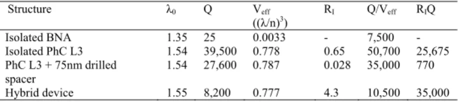
vides a compa mponents. The Veff compared
red to the hybr would not be why the merit o d RIQ are als
RI is simply th
e cases.
pot is created a y (|Ey|2) along
t the BNA. The transferred fr he total power e guide. The opti
s larger when th
plot of the optica hybrid cavity is e ntensity pattern in line passing throug e structure is excite
to the hybrid d field) is set to ximately 17% ing its excitat metallic nanoa
e used (as opp sy optics and th ensity. In the 60 times higher arison between e hybrid struct to the isolated rid structure, bu suitable for st of certain devic o quoted for he ratio of the at the BNA ga a vertical lin e optical inten from the wave exiting through ical intensity o
he BNA is pre
al intensity (|Ey|2) i excited via a W1 n the BNA region. gh the center of th ed with a W1 wav
device using th o −0.76dB for t
of the input li tion very ener antennas illum
posed to a hyb he light at the B proposed hyb r than the optic n the characte ture has a high d PhC cavity. T
ut does not pro tudying single-ces should not the two PhC intensity at th ap as shown in ne passing thro nsity in each si eguide to the h the waveguid on top of the st sent compared in the xy plane at PhC waveguide. Comparison of th he structure with ( veguide. he W1 wavegu the fundamenta ight in the wa rgy efficient c minated vertic brid photonic-BNA gap reach brid device, w cal intensity on eristics of the her Q compare The isolated P ovide an extern -molecule inter t be determined resonator stru he surface to t
n Fig. 5(a). Fig ough the cent imulation is no
hybrid cavity de from the tot tructure (at the d to when it is n
the top surface of (b) The expanded he optical intensity (blue) and without
uide, the S21 p al resonant mo aveguide coupl compared to s cally. When a -plasmonic dev hes enhanceme we can achiev n top of the PhC hybrid device ed to the isola PhC cavity has nally accessible ractions. This d by consideri uctures in Tab that at the cent
gure 5(b) ter of the ormalized y. This is tal power e position not. f d y t parameter ode of the les into a structures arrays of vice), the ents up to ve optical C cavity. e and its ated BNA s a higher e hot-spot is a good ng Q/Veff ble 1 for ter of the
Table 1. Comparison of λ0, Q, Veff, Q/Veff and RIQ of the device at different design stages. Structure λ0 Q Veff ((λ/n)3) RI Q/Veff RIQ Isolated BNA 1.35 25 0.0033 - 7,500 - Isolated PhC L3 1.54 39,500 0.778 0.65 50,700 25,675 PhC L3 + 75nm drilled spacer 1.54 27,600 0.787 0.028 35,000 770 Hybrid device 1.55 8,200 0.777 4.3 10,500 35,000 8. Discussions
We envisage the development of hand-held, application-specific platforms with highly integrated arrays of hybrid optical resonators. Such platforms would produce patterns of nano-sized optical hot-spots on a smooth surface and be illuminated and interrogated via a hidden network of waveguides. The successful realization of this platform will contribute to advances in many fields, including chemistry, life sciences, personalized medicine and quantum information technology.
The ability of the hybrid resonator to trap on the nanoscale allows individual molecules and nanoparticles to be controlled and studied. The BNA hot-spot in the hybrid device has approximately 40 times higher intensity than the evanescent field at the surface of a conventional PhC cavity. Furthermore, the intensity gradient is as important as the intensity and enters directly into the Maxwell stress tensor describing optical forces. The high intensity in the BNA gap and nanoscale localization produce very large intensity gradients around the hot-spot, including a positive vertical gradient, which eliminates the force drawing trapped particles down onto the PhC surface and replaces it with an upward force drawing the particles back into the hot-spot. At the same time, when the hybrid resonator is pumped through a waveguide, it only delivers light to the BNA and suppresses the unwanted illumination of the specimen across the rest of the surface. For the region without the BNA, the SiO2 spacing layer further reduces the surface evanescent field of the waveguides,
offering additional control over the parasitic trapping and guiding of particles.
Conventional optical manipulation and nanoplasmonic trapping setups are very energy inefficient where most of the light is lost passing through the bulk optics or by illuminating a large proportion of the glass substrate rather than just the BNAs. The ability to couple the hybrid resonator to an optical waveguide is a key attribute of this device, which greatly improves its efficiency and allows the unused energy to be used by devices downstream. The coupling between the waveguide and the hybrid device can be controlled by tailoring the design of the waveguide and its distance from the cavity to adjust the number of hybrid devices that can be powered and characterized using a single waveguide. Using the W1 waveguide design in this paper, about 16% of the input light is coupled into the hybrid cavity, about 2% of which is concentrated in the BNA hot-spot. By properly engineering the waveguide-cavity coupling coefficients, this waveguide could support the uniform excitation of four hybrid cavities.
The resonances of the devices can be individually tuned by small changes to the PhC cavity. Thus, light can be selectively delivered to specific resonators by tuning the excitation to the appropriate wavelength, allowing unprecedented control over the optical potential surface of the sample and making it possible to perform many different (or identical) single molecule experiments simultaneously. By facilitating parallel experiments, the platform will reduce the time and effort needed to collect enough data to draw statistically valid conclusions. At the same time, it will reduce the cost, time and complexity of the experiments, while simultaneously increasing experimental control and accuracy.
Finally, as a highly integrated, fiber-connected platform, it will be simple and ideal for coupling to micro- and nanofluidic systems for the delivery of the molecules and particles and bespoke optical interrogation systems based on photonic integrated circuits. The flat surface
of this device will minimize the unintended adhesion of molecules to morphological surface features and simplify the use of surface treatments and application specific coatings.
9. Summary and conclusions
This paper addresses the design of a hybrid photonic-plasmonic resonator as the key building block of a multicomponent platform for high-throughput, single-molecule experiments. The hybrid device is comprised of an L3 PhC cavity coupled to a BNA, with a SiO2 layer
separating the BNA from the PhC cavity. By defining a new FOM that is more appropriate for our target application, the thickness of the spacer layer is optimized to maximize the energy in the BNA gap for a given input power. The device produces an externally accessible hot-spot, whose intensity is 40-60 times larger than that of the evanescent field at the surface of an isolated PhC cavity and at least 4.3 times larger than the intensity at the center of the PhC cavity. The optical intensity gradient (often a more important parameter than the optical intensity) created around the hot-spot in the BNA gap will contribute significantly to its trapping performance for nanoparticles. Finally, the hybrid resonator can be excited via a PhC waveguide, greatly improving its energy efficiency and making it compatible with user-friendly fiber-optic and photonic integrated circuit technologies. Thus, when successfully fabricated, this hybrid resonator will allow the realization of an integrated platform suitable of conducting a large number of single-molecule experiments simultaneously.
Funding
Engineering and Physical Sciences Research Council [grant number EP/H024891/1].
Acknowledgements
This work was supported by the Engineering and Physical Sciences Research Council [grant number EP/H024891/1]. M. Mossayebi gratefully acknowledges the support of the University of Nottingham under the Dean of Engineering scholarship for international excellence and the Building Experience and Skill Travel Scholarships.
References
1. K. C. Neuman and A. Nagy, “Single-molecule force spectroscopy: optical tweezers, magnetic tweezers and atomic force microscopy,” Nat. Methods 5(6), 491–505 (2008).
2. K. C. Neuman and S. M. Block, “Optical trapping,” Rev. Sci. Instrum. 75(9), 2787–2809 (2004).
3. P. T. Kristensen, C. Van Vlack, and S. Hughes, “Generalized effective mode volume for leaky optical cavities,” Opt. Lett. 37(10), 1649–1651 (2012).
4. J. A. Schuller, E. S. Barnard, W. Cai, Y. C. Jun, J. S. White, and M. L. Brongersma, “Plasmonics for extreme light concentration and manipulation,” Nat. Mater. 9(3), 193–204 (2010).
5. A. Kinkhabwala, Z. Yu, S. Fan, Y. Avlasevich, K. Müllen, and W. Moerner, “Large single-molecule fluorescence enhancements produced by a bowtie nanoantenna,” Nat. Photonics 3(11), 654–657 (2009). 6. M. L. Juan, M. Righini, and R. Quidant, “Plasmon nano-optical tweezers,” Nat. Photonics 5(6), 349–356 (2011). 7. B. J. Roxworthy, K. D. Ko, A. Kumar, K. H. Fung, E. K. Chow, G. L. Liu, N. X. Fang, and K. C. Toussaint, Jr.,
“Application of plasmonic bowtie nanoantenna arrays for optical trapping, stacking, and sorting,” Nano Lett.
12(2), 796–801 (2012).
8. N. A. Hatab, C. H. Hsueh, A. L. Gaddis, S. T. Retterer, J. H. Li, G. Eres, Z. Zhang, and B. Gu, “Free-standing optical gold bowtie nanoantenna with variable gap size for enhanced Raman spectroscopy,” Nano Lett. 10(12), 4952–4955 (2010).
9. J. N. Anker, W. P. Hall, O. Lyandres, N. C. Shah, J. Zhao, R. P. Van Duyne, “Biosensing with plasmonic nanosensors”, In Nanoscience And Technology: A Collection of Reviews from Nature Journals, 308–319 (2010).
10. P. Mestres, J. Berthelot, S. S. Aćimović, and R. Quidant, “Unraveling the optomechanical nature of plasmonic trapping,” Light Sci. Appl. 5(7), e16092 (2016).
11. Y. Pang and R. Gordon, “Optical trapping of a single protein,” Nano Lett. 12(1), 402–406 (2012). 12. J. D. Joannopoulos, P. R. Villeneuve, and S. Fan, “Photonic crystals: putting a new twist on light,” Nature
386(6621), 143–149 (1997).
13. G. Magno, M. Fevrier, P. Gogol, A. Aassime, A. Bondi, R. Mégy, and B. Dagens, “Strong coupling and vortexes assisted slow light in plasmonic chain-SOI waveguide systems,” Sci. Rep. 7(1), 7228 (2017).
14. D. Conteduca, F. Dell’Olio, T. F. Krauss, and C. Ciminelli, “Photonic and plasmonic nanotweezing of nano-and microscale particles,” Appl. Spectrosc. 71(3), 367–390 (2017).
15. M. Kamandar Dezfouli and S. Hughes, “Quantum optics model of surface-enhanced Raman spectroscopy for arbitrarily shaped plasmonic resonators,” ACS Photonics 4(5), 1245–1256 (2017).
16. E. Bermúdez-Ureña, G. Tutuncuoglu, J. Cuerda, C. L. C. Smith, J. Bravo-Abad, S. I. Bozhevolnyi, A. Fontcuberta I Morral, F. J. García-Vidal, and R. Quidant, “Plasmonic Waveguide-Integrated Nanowire Laser,” Nano Lett. 17(2), 747–754 (2017).
17. F. Todisco, M. Esposito, S. Panaro, M. De Giorgi, L. Dominici, D. Ballarini, A. I. Fernández-Domínguez, V. Tasco, M. Cuscunà, A. Passaseo, C. Ciracì, G. Gigli, and D. Sanvitto, “Toward cavity quantum electrodynamics with hybrid photon gap-plasmon states,” ACS Nano 10(12), 11360–11368 (2016).
18. M. Bahramipanah, S. Dutta-Gupta, B. Abasahl, and O. J. F. Martin, “Cavity-Coupled Plasmonic Device with Enhanced Sensitivity and Figure-of-Merit,” ACS Nano 9(7), 7621–7633 (2015).
19. S. Cui, X. Zhang, T. Liu, J. Lee, D. Bracher, K. Ohno, D. Awschalom, and E. L. Hu, “Hybrid plasmonic photonic crystal cavity for enhancing emission from near-surface nitrogen vacancy centers in diamond,” ACS Photonics 2(4), 465–469 (2015).
20. S. Mokkapati, D. Saxena, N. Jiang, L. Li, H. H. Tan, and C. Jagadish, “An order of magnitude increase in the quantum efficiency of (Al)GaAs nanowires using hybrid photonic-plasmonic modes,” Nano Lett. 15(1), 307–312 (2015).
21. M. Castro-Lopez, N. de Sousa, A. Garcia-Martin, F. Y. Gardes, and R. Sapienza, “Scattering of a plasmonic nanoantenna embedded in a silicon waveguide,” Opt. Express 23(22), 28108–28118 (2015).
22. Y. Luo, M. Chamanzar, A. Apuzzo, R. Salas-Montiel, K. N. Nguyen, S. Blaize, and A. Adibi, “On-chip hybrid photonic-plasmonic light concentrator for nanofocusing in an integrated silicon photonics platform,” Nano Lett.
15(2), 849–856 (2015).
23. A. El Eter, N. M. Hameed, F. I. Baida, R. Salut, C. Filiatre, D. Nedeljkovic, E. Atie, S. Bole, and T. Grosjean, “Fiber-integrated optical nano-tweezer based on a bowtie-aperture nano-antenna at the apex of a SNOM tip,” Opt. Express 22(8), 10072–10080 (2014).
24. Z. Li, J. Kou, M. Kim, J. O. Lee, and H. Choo, “Highly efficient and tailorable on-chip metal–insulator–metal plasmonic nanofocusing cavity,” ACS Photonics 1(10), 944–953 (2014).
25. I. Mukherjee and R. Gordon, “Analysis of hybrid plasmonic-photonic crystal structures using perturbation theory,” Opt. Express 20(15), 16992–17000 (2012).
26. M. Xi and B. M. Reinhard, “Localized surface plasmon coupling between mid-IR-resonant ITO nanocrystals,” J Phys Chem C Nanomater Interfaces 122(10), 5698–5704 (2018).
27. X. Yang, A. Ishikawa, X. Yin, and X. Zhang, “Hybrid photonic-plasmonic crystal nanocavities,” ACS Nano
5(4), 2831–2838 (2011).
28. M. Chamanzar and A. Adibi, “Hybrid nanoplasmonic-photonic resonators for efficient coupling of light to single plasmonic nanoresonators,” Opt. Express 19(22), 22292–22304 (2011).
29. X. He, L. Yang, and T. Yang, “Optical nanofocusing by tapering coupled photonic-plasmonic waveguides,” Opt. Express 19(14), 12865–12872 (2011).
30. R. F. Oulton, V. J. Sorger, D. Genov, D. Pile, and X. Zhang, “A hybrid plasmonic waveguide for subwavelength confinement and long-range propagation,” Nat. Photonics 2(8), 496–500 (2008).
31. A. L. Pyayt, B. Wiley, Y. Xia, A. Chen, and L. Dalton, “Integration of photonic and silver nanowire plasmonic waveguides,” Nat. Nanotechnol. 3(11), 660–665 (2008).
32. F. De Angelis, M. Patrini, G. Das, I. Maksymov, M. Galli, L. Businaro, L. C. Andreani, and E. Di Fabrizio, “Nanoscale chemical mapping using three-dimensional adiabatic compression of surface plasmon polaritons,” Nano Lett. 8(8), 2321–2327 (2008).
33. M. Barth, S. Schietinger, S. Fischer, J. Becker, N. Nüsse, T. Aichele, B. Löchel, C. Sönnichsen, and O. Benson, “Nanoassembled plasmonic-photonic hybrid cavity for tailored light-matter coupling,” Nano Lett. 10(3), 891– 895 (2010).
34. T. Zhang, S. Callard, C. Jamois, C. Chevalier, D. Feng, and A. Belarouci, “Plasmonic-photonic crystal coupled nanolaser,” Nanotechnology 25(31), 315201 (2014).
35. A. E. Eter, T. Grosjean, P. Viktorovitch, X. Letartre, T. Benyattou, and F. I. Baida, “Huge light-enhancement by coupling a Bowtie Nano-antenna’s plasmonic resonance to a photonic crystal mode,” Opt. Express 22(12), 14464–14472 (2014).
36. M. Mossayebi, G. Bellanca, A. Parini, A. J. Wright, and E. C. Larkins, “Engineering of Hybrid Photonic-Plasmonic Devices for Enhanced Light-Matter Interactions”, In Recent Trends in Computational Photonics, Springer, Cham., 369–390 (2017).
37. M. Mossayebi, A. J. Wright, A. Parini, M. G. Somekh, G. Bellanca, and E. C. Larkins, “Investigating the use of a hybrid plasmonic–photonic nanoresonator for optical trapping using finite-difference time-domain method,” Opt. Quantum Electron. 48(5), 275 (2016).
38. F. Zhang, J. Ren, X. Duan, Z. Chen, Q. Gong, and Y. Gu, “Evanescent-field-modulated two-qubit entanglement in an emitters-plasmon coupled system,” J. Phys. Condens. Matter 30(30), 305302 (2018).
39. C. Ciminelli, D. Conteduca, F. Dell’Olio, and M. Armenise, “Design of an optical trapping device based on an ultra-high Q/V resonant structure,” IEEE Photonics J. 6(6), 1–16 (2014).
40. C. Sauvan, P. Lalanne, and J. P. Hugonin, “Slow-wave effect and mode-profile matching in photonic crystal microcavities,” Phys. Rev. B Condens. Matter Mater. Phys. 71(16), 165118 (2005).
41. W. Yu-Ming, L. Le-Wei, and L. Bo, “Geometric effects in designing bow-tie nanoantenna for optical resonance investigation.”, Electromagnetic Compatibility (APEMC), 2010 Asia- Pacific Symposium on, 1108–1111 (2010).
42. H. Chen, A. M. Bhuiya, R. Liu, D. M. Wasserman, and K. C. Toussaint, Jr., “Design, fabrication, and characterization of near-IR gold bowtie nanoantenna arrays,” J. Phys. Chem. C 118(35), 20553–20558 (2014). 43. S. Malaguti, G. Bellanca, L. Ottaviano, K. Yvind, S. Combrié, A. De Rossi, and S. Trillo, “Tailored design of
WDM filters in BCB embedded PhC membranes,” Opt. Quantum Electron. 45(4), 329–342 (2013). 44. LumericalSolutions, Inc., http://www.lumerical.com/tcad-products/fdtd/.
45. P. B. Johnson and R. W. Christy, “Optical constants of the noble metals,” Phys. Rev. B 6(12), 4370–4379 (1972).
46. A. C. Lesina, A. Vaccari, P. Berini, and L. Ramunno, “On the convergence and accuracy of the FDTD method for nanoplasmonics,” Opt. Express 23(8), 10481–10497 (2015).