Research Article
A Transfer Hamiltonian Model for Devices
Based on Quantum Dot Arrays
S. Illera, J. D. Prades, A. Cirera, and A. Cornet
MIND/IN2UB Departament d’Electr`onica, Universitat de Barcelona, C/Mart´ı i Franqu`es 1, 08028 Barcelona, Spain Correspondence should be addressed to S. Illera; [email protected]
Received 16 December 2014; Accepted 19 February 2015 Academic Editor: Michael L. P. Tan
Copyright © 2015 S. Illera et al. This is an open access article distributed under the Creative Commons Attribution License, which permits unrestricted use, distribution, and reproduction in any medium, provided the original work is properly cited.
We present a model of electron transport through a random distribution of interacting quantum dots embedded in a dielectric matrix to simulate realistic devices. The method underlying the model depends only on fundamental parameters of the system and it is based on the Transfer Hamiltonian approach. A set of noncoherent rate equations can be written and the interaction between the quantum dots and between the quantum dots and the electrodes is introduced by transition rates and capacitive couplings. A realistic modelization of the capacitive couplings, the transmission coefficients, the electron/hole tunneling currents, and the density of states of each quantum dot have been taken into account. The effects of the local potential are computed within the self-consistent field regime. While the description of the theoretical framework is kept as general as possible, two specific prototypical devices, an arbitrary array of quantum dots embedded in a matrix insulator and a transistor device based on quantum dots, are used to illustrate the kind of unique insight that numerical simulations based on the theory are able to provide.
1. Introduction
The demand for increasing the integrated density devices has led to the emergency of a whole generation devices based on confined structures. The MOS (metal-oxide-semiconductor) transistor is the archetype of a confined two-dimensional system [1]. Nevertheless, the possibility to enhance this confinement by embedding low-dimensional structures in an insulating matrix has opened new way for further downscaling. Compared to the standard bulk technology, the corresponding devices based on these structures have increased the structural and conceptual complexity. These structures (quantum dots, wires, or layers) can be used in single-electron devices [2], new memory concepts [3], and photo- or electroluminescent devices [4]. Concerning single-electron devices, they are currently conceived to take advan-tage of tunnel current between quantum states belonging to nanoscale particles [5,6]. The single-electron devices based on quantum dots (Qds) appear to be potential candidates to improve, to complete, or even to replace the current MOS technology with which they may remain compatible. In order to be able to asses the potentials and capabilities of
the various novel devices, a realistic theoretical estimation of the specific device performance is thus highly desirable. Within this context, the simulations of such devices must be performed not only to understand but also to predict experimental behaviors. Moreover, from a physical point of view, we will learn a lot from these simulations if they are independent of high-level experimental parameters (as tunneling rates, defective interfaces,. . ., etc.) and are based on low-level concrete ones (geometrical data, barrier height. . .). Concerning Qds, they are particularly attractive because they possess discrete energy levels and quantum properties similar to natural atoms or molecules due to the strong con-finement in all three directions. This fact affects dramatically the electronic transport properties. Until now, research has mostly concentrated on single Qds and many novel transport phenomena have been discovered, such as the staircaselike current-voltage (𝐼-𝑉) characteristic [7], Coulomb blockade oscillation [8], negative differential capacitance [9], and the Kondo effect [10].
From experimental point of view, rapid progress in microfabrication technology has made possible coupling Qds system with aligned levels [11–13]. In fact, the use of
the Coulomb blockade phenomenon in systems made up of combinations of tunnel junctions and semiconductor Qds seems to offer promising perspectives, in particular in non-volatile memory applications and also for single-electron transistor [14]. Moreover, the concept of multi-dot memory using semiconductor nanocrystals embedded in an insulator matrix as floating-gate has already been demonstrated [15] and the quantization effects have been used in self-aligned double-stacked memory to improve the retention time [16].
From a theoretical perspective, researchers have recently paid much attention to electron transport through several Qds, since multiple Qd provides more Feynman paths for the electron transmission [17]. The complexity of structure and physical mechanism and the prominent role of dimensional and quantum effects characterizing the operation of these novel Qds devices preclude the use of standard macroscopic bulk semiconductor transport theory. Many authors have studied the electron transport using NEGFF (nonequilibrium Green functions formalism) [18,19], taking into account the potential due to the self-charge. However, up to now nobody has done a computation of transport in an extended arbitrary array of Qds using this framework since this approach is usually unfeasible to implement for large systems. On the other hand, rate equation type models used for lasers or light-emitting diodes often offer a satisfactory description of the charge transport. Moreover, this approach presents a more transparent vision of the electron transport. Thus, this model is easier to tinker with, in order to deal with more complicated nanostructures based on Qds.
In this work, we present in full a model based on noncoherent rate equations [20], which is suitable to study the electron transport in Qd arrays. In a previous work [21], a preliminary version of this methodology was presented and used to obtain analytical solutions for electron trans-port in simple cases. The methodology was also compared with nonequilibrium Green’s function calculations, obtaining favorable results [22]. Despite the simplicity of the model, it provided good results and it was also easily scalable.
Now, a complete model to simulate devices based on Qd arrays is presented. This model creates a compact modeling tool to study and simulate the electronic transport as a func-tion of geometrical and basic material parameters, making possible to use it as a device design tool. The theoretical formalism and the assumptions made in the model are thoroughly described. The interaction between Qds and between these and the leads has been introduced by transition rates and capacitive couplings. The local potential effects were computed self-consistently. Inelastic and backscattering effects were neglected. Concerning the transition rates, the use of ab initio calculations is shown to be the best way to fully understand the underlaying tunneling physics in nanostructures. However, if first-principles calculations for single tunnel events were implemented, the huge effort required would make the simulation time increase in an unacceptable manner. This impractical computational time forced us to write a compact model with some assumptions and relax the expectation of accuracy when treating with few-electron devices operating through quantum features.
Specifically, we used the one-dimensional WKB approxima-tion, which neglects spatial variation of the wavefunction over the nontransport directions to describe the tunnel processes. The hole transport was also introduced obtaining new current terms and realistic expressions for the capacity in bipolar conduction. All of these have been implemented in a computational code conforming a powerful transport simulation tool that allows reproducing, explaining, and predicting the behavior of multiple devices based on Qds. Furthermore, we also present details about the computational implementation. Finally, in order to show the capabilities of the presented methodology, two examples of practical implementations of Qd-based devices were simulated: one single Qd and a multilayer structure that conform the basic building block of future devices based on Qds.
2. The Model
As in any device simulation, the ultimate goal of the presented approach is the prediction of the device response of one specific architecture (geometry, material,. . ., etc.) to a given variation in the external conditions (bias voltage) via the solution of the dynamical equations. First of all, we are going to describe the device architecture and, after that, we write the underlying equations.
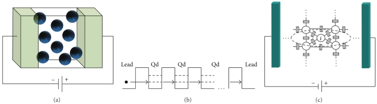
2.1. The Structure. Figure 1(a)shows the basic building blocks of our device which is in essence an insulator layer sand-wiched between two metallic electrodes. Inside the insulator layer, a random distribution of𝑁 Qds can be inserted. This is the classical structure that is obtained due to the fabrication processes, a superlattice of insulator-semiconductor bilayers. Although a single connected Qd to the leads has been obtained creating a so-called single electron transistor (SET) [29], the research mainstream is focused on the properties of structures with many Qds to create nonvolatile memories [30], light-emitting devices [31], or solar cells devices [32].
Due to the fabrication processes, the insulator thickness is large enough to avoid direct tunneling between the electrodes (or leads). Therefore, the electron current needs to pass through the Qds. InFigure 1(b)the energy band diagram of the system is shown. The Qds are presented as potential wells in the dielectric energy band and they assist the tunneling processes. Thus, a correct description of the tunneling pro-cesses among the Qds and Qds-electrodes is needed. These tunneling processes can be described by tunnel junctions. From the electrical point of view, a single tunnel junction is described by a capacitance and a current source that depends on the voltage drop in the junction. The equivalent electrical circuit is shown inFigure 1(c)for an arbitrary Qd array.
From the electrical scheme, two coupling equations gov-ern the response of the system: on one hand we can write the charge conservation in each Qd. In the steady state, the charge conservation for this system is analogous to the electronic Kirchhoff ’s current law. Thus, using the decomposition of the tunneling junctions in current sources, we can write
0 = ∑
− + (a) Qd Qd Qd Lead Lead · · · (b) + − · · · · .. . ... .. . .. . i (c)
Figure 1: (a) The basic building block that forms the devices based on Qds: an array of Qds (they could be ordered or randomly dispersed) embedded in an insulator matrix sandwiched between two electrodes (leads). (b) Energy band scheme of the structure. The electron starts in the left lead and crosses through the dielectric matrix by tunneling processes assisted by the intermediate Qds. (c) Scheme of the equivalent electrical circuit of the device presented in (a). The Qds (circles) are connected between them and the leads (color blocks) by tunneling junctions. The tunneling junction is described as a capacitor in parallel with a current source.
for the 𝑖th Qd (equivalent to a node), where 𝑁 is the number of Qds and the summation takes into account all the linked elements to this Qd. On the other hand, the current through a junction will depend on the voltage drop in the tunneling junction. Therefore, a second equation is necessary to describe the voltage in each Qd, the same as the Kirchhoff ’s voltage law. First of all, we are going to show analytical expressions for the tunnel currents through a junctions and, after that, we will calculate the potential in each Qd using the Poisson equation.
2.2. Current through a Tunneling Junction. A usual method employed to describe the tunneling processes in devices is the tunneling Hamiltonian approach (also called Transfer Hamiltonian approach). This theory, thoroughly studied by many authors [33–35], treats the tunnelling events as a perturbation. The matrix coefficient |𝑇𝐿𝑅|2 quantifies the probability for a particle to transfer from a state of the left side of the barrier to a state of the right side by a tunnel process.
The tunneling rate is determined using time-dependent perturbation theory by considering the electron from one side of the barrier as initial state and the electron on the other side as a final state. The tunneling rate from the left to the right states (both are considered as a part of a continuum) can be calculated using the Fermi’s golden rule [36]:
𝑑2𝑊⃗𝑘𝐿→ ⃗𝑘𝑅= 2𝜋ℏ 𝑇𝐿𝑅2𝜌𝑅(𝐸𝑅) 𝜌𝐿(𝐸𝐿) 𝛿 (𝐸𝑅− 𝐸𝐿) 𝑑𝐸𝑅𝑑𝐸𝐿, (2) where𝜌𝐿and𝜌𝑅are the density of states of the left and right side. From this expression, we can see that we only consider ballistic transport. This means that the electron does not suffer energy loss scattering processes when it moves through the barrier. Introducing the energy distribution function in each part of the barrier we can evaluate the total tunneling
rate from all occupied states on the left to all unoccupied states on the right [37]:
Γ𝐿 → 𝑅= ∫+∞ −∞ 𝜌𝐿(𝐸𝐿) 𝑓𝐿(𝐸𝐿) ⋅ {∫+∞ −∞ 2𝜋 ℏ 𝑇𝐿𝑅 2[1 − 𝑓 𝑅(𝐸𝑅)] ⋅ 𝜌𝑅(𝐸𝑅) 𝛿 (𝐸𝑅− 𝐸𝐿) 𝑑𝐸𝑅} 𝑑𝐸𝐿. (3)
The opposite tunneling rate can be calculated in a similar way. Thus, the net tunneling current𝐼 = −𝑞[Γ𝐿 → 𝑅− Γ𝑅 → 𝐿] assuming symmetry in the transmission coefficient𝑇𝐿𝑅 = 𝑇𝑅𝐿[38] can be written as 𝐼𝑅𝐿= 4𝜋𝑞 ℏ ∫ +∞ −∞ 𝑇𝑅𝐿(𝐸) 2𝜌 𝑅(𝐸) 𝜌𝐿(𝐸) [𝑓𝑅(𝐸) − 𝑓𝐿(𝐸)] 𝑑𝐸, (4) where we introduce a factor of 2 to take into account the spin. Therefore, using this approach, we can describe the whole system as independent subsystems (the Qds) connected between them by a transmission probability through the dielectric media. Thus, this methodology allows us to write the currents between the different parts of the system.
In the above expressions, 𝑓𝑅 and 𝑓𝐿 are the nonequi-librium energy distribution functions in each side of the barrier. These distributions functions take into account how the energy levels are filled (𝑓𝑅) or emptied (1 − 𝑓𝑅); as it is expected the electron transport only occurs if the initial state is filled and the final state is empty (see(3)). However, the distribution function of each part of the system is unknown. Assuming that the distribution functions of the electrodes (left𝐿 and right 𝑅 electrodes) are well described by the equilibrium Fermi Dirac statistics using modified electrochemical potentials,𝜇𝐿 − 𝜇𝑅 = 𝑞𝑉 where 𝑉 is the applied bias voltage, the problem is reduced to find the nonequilibrium distributions functions of each Qd (𝑛𝑖).
From the definition of the total charge,𝑁𝑖inside the𝑖th Qd can be expressed as
𝑁𝑖= ∫ 𝜌𝑖(𝐸) 𝑛𝑖(𝐸) 𝑑𝐸. (5)
Here, we are going to redefine the notation used to describe the distribution functions. The distribution function for each Qd is 𝑛𝑖 while we reserve 𝑓𝐿 and 𝑓𝑅 for the distribution function of the left and right leads, respectively. We can write the evolution charge in time for each Qd as𝑁𝑖 = ∑𝑗∫ 𝐼𝑗𝑖𝑑𝑡, where the subscript 𝑗 takes into account all the elements that are linked to the 𝑖th Qd. Thus, from(5)we can write the evolution of charge in time as a function of the total net current flux for each Qd. This set of integrodifferential equations has a similar form as a usual rate equation. In the following, the different current terms and the elements that appear in(4)are going to be discussed.
2.2.1. Electron and Holes Current Terms. Since the evolution charge in time of each Qd can be written as a function of the net current flux, it is needed to determine all the current contributions. The current contributions can be of two types; the Qds have leads contributions and also neighbors Qd
current contributions. These two types of current have the same form in(4), but in each case we need to use the correct distribution function.
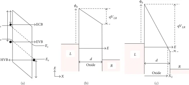
From the point of view of the nature of these contribu-tions, we have three different processes [39]. InFigure 2(a)
we show the scheme of the different tunneling processes. The first term corresponds to electron tunneling from conduction band to conduction band (ECB). The second one is an electron tunneling from valence band to conduction band (EVB). Since the transmission coefficients are symmetric, this process also involves the inverse case, tunneling from conduction band to valence band. The last process is related to the holes: hole tunneling from valence band to valence band (HVB).
One important point is how we treat the distinction between electrons and holes. From a physical point of view, the hole conduction can be viewed as electron conduction restricted to the valence band. Therefore, we can consider only electron transport but taking into account the conduc-tion and valence band contribuconduc-tions to the current. Thus, we only need to consider the changing number of electrons in these two bands. Therefore, the time charge evolution equations for each Qd can be written as
𝑑𝑁𝑖 𝑑𝑡 = ∫ +∞ −∞ 𝑇ECB 2𝜌 𝐿𝜌𝑖CB(𝑓𝐿− 𝑛𝑖)𝑑𝐸 + ∫ +∞ −∞ 𝑇HVB 2𝜌 𝐿𝜌𝑖VB(𝑓𝐿− 𝑛𝑖)𝑑𝐸 ⏟⏟⏟⏟⏟⏟⏟⏟⏟⏟⏟⏟⏟⏟⏟⏟⏟⏟⏟⏟⏟⏟⏟⏟⏟⏟⏟⏟⏟⏟⏟⏟⏟⏟⏟⏟⏟⏟⏟⏟⏟⏟⏟⏟⏟⏟⏟⏟⏟⏟⏟⏟⏟⏟⏟⏟⏟⏟⏟⏟⏟⏟⏟⏟⏟⏟⏟⏟⏟⏟⏟⏟⏟⏟⏟⏟⏟⏟⏟⏟⏟⏟⏟⏟⏟⏟⏟⏟⏟⏟⏟⏟⏟⏟⏟⏟⏟⏟⏟⏟⏟⏟⏟⏟⏟⏟⏟⏟⏟⏟⏟⏟⏟⏟⏟⏟⏟⏟⏟⏟⏟
Left lead contribution
+ ∫+∞ −∞ |𝑇ECB| 2𝜌 𝑅𝜌𝑖CB(𝑓𝑅− 𝑛𝑖)𝑑𝐸 + ∫ +∞ −∞ 𝑇HVB 2𝜌 𝑅𝜌𝑖VB(𝑓𝑅− 𝑛𝑖)𝑑𝐸 ⏟⏟⏟⏟⏟⏟⏟⏟⏟⏟⏟⏟⏟⏟⏟⏟⏟⏟⏟⏟⏟⏟⏟⏟⏟⏟⏟⏟⏟⏟⏟⏟⏟⏟⏟⏟⏟⏟⏟⏟⏟⏟⏟⏟⏟⏟⏟⏟⏟⏟⏟⏟⏟⏟⏟⏟⏟⏟⏟⏟⏟⏟⏟⏟⏟⏟⏟⏟⏟⏟⏟⏟⏟⏟⏟⏟⏟⏟⏟⏟⏟⏟⏟⏟⏟⏟⏟⏟⏟⏟⏟⏟⏟⏟⏟⏟⏟⏟⏟⏟⏟⏟⏟⏟⏟⏟⏟⏟⏟⏟⏟⏟⏟⏟⏟⏟⏟⏟⏟⏟⏟
Right lead contribution
, Neighboring Qds contribution { { { { { { { { { { { { { +∑𝑁 𝑗,𝑗 ̸=𝑖 {∫+∞ −∞ 𝑇ECB 2𝜌BC 𝑖 𝜌𝑗BC(𝑛𝑗− 𝑛𝑖) 𝑑𝐸 + ∫ +∞ −∞ 𝑇HVB 2𝜌VB 𝑖 𝜌𝑗VB(𝑛𝑗− 𝑛𝑖) 𝑑𝐸} +∑𝑁 𝑗,𝑗 ̸=𝑖 {∫+∞ −∞ 𝑇EVB 2𝜌BC 𝑖 𝜌𝑗VB(𝑛𝑗− 𝑛𝑖) 𝑑𝐸 + ∫ +∞ −∞ 𝑇EVB 2𝜌BC 𝑗 𝜌𝑖VB(𝑛𝑗− 𝑛𝑖) 𝑑𝐸} , (6)
where𝑖 = 1 ⋅ ⋅ ⋅ 𝑁 and we take into account all the contri-butions for an arbitrary𝑖th Qd. The first pair of elements is related to the left lead contribution and the electron and the hole contributions. For simplicity, we assume infinite metallic leads; therefore, we only write the continuum DOS of the leads (𝜌𝐿); meanwhile, in the Qd we write the DOS in separate terms, conduction (𝜌BC
𝑖 ) and valence (𝜌𝑖VB) bands. In the next
section, we will show that the Qds have discrete electron/hole energy levels instead of conduction or valence bands but this expression will not change. Similar contribution is obtained for the right lead. In these two contributions we use the Fermi Dirac distribution function to describe the leads with 𝜇𝐿− 𝜇𝑅= −𝑞𝑉𝑑𝑠electrochemical potentials. In each current term, we use the appropriate transmission coefficient. The last two pairs of current terms represent the current from the neighbor Qds. The subscript “𝑗” runs over all the Qds except the Qd that we are considering. In these terms we
take into account the different processes, tunneling from the conduction band (CB) to conduction band (CB) and tunneling from valence band (VB) to valence band (VB). We also need to describe the tunneling that mixes the bands (EVB processes) in two ways, from CB to VB and from VB to CB. As it is easy to see, these processes cannot occur at the same time but it is important to take both into account.
The set of equations,(6), can be solved for the steady state. Under our assumption that there is no inelastic scattering, the system can be written in a matrix form and solved for each energy step to obtain the nonequilibrium distribution function for each Qd (𝑛𝑖).
2.2.2. Transmission Coefficients. From(2) the transmission
coefficient|𝑇𝐿𝑅|2is defined as the tunnel probability of the electrons crossing through the dielectric media. The tunnel-ing probability is a strong function of the parallel component
ECB EVB HVB Ec Ec E𝜐 E𝜐 (a) E E L R Oxide 𝜙0 X d qVLR (b) E L R Oxide X2 d qVLR 𝜙0 (c)
Figure 2: (a) Schematics of the different tunneling processes. Electron from conduction band to conduction band (ECB), electron from valence band to conduction band (EVB), and tunneling from valence band to valence band (HVB) processes. Energy band diagram for the tunneling processes under polarization. (b) If the incident electron energy (𝐸) is less than the modified energy barrier (𝑞𝜙0− 𝑞𝑉𝐿𝑅) we use a direct tunnel expression. (c) If the incident electron energy (𝐸) is greater than the modified energy barrier (𝑞𝜙0− 𝑞𝑉𝐿𝑅), we use a
Fowler-Nordheim expression. These expressions depend on the incident electron energy but also depend on the polarization voltage.
to the junction interface energy𝐸‖. At each particular total energy 𝐸, the DOS with a zero 𝐸‖ component is heavily weighted by the tunneling probability in(4). Therefore the DOS only takes into account states with 𝑘‖ ≈ 0. This approximation may in part be a justification for ignoring the tunneling electron momentum in(3)[40].
Under our assumptions, we use the semiclassical and one-dimensional WKB approximation [36] for the transmission coefficient|𝑇(𝐸)|2: |𝑇 (𝐸)|2= exp {−2ℏ∫𝑥2 𝑥1 √2𝑚∗ diel(𝑉 (𝑥) − 𝐸)𝑑𝑥 } , (7)
where𝑥1and𝑥2are the classical turning points,𝑚∗diel is the effective dielectric mass, and𝑉(𝑥) is the potential barrier of the dielectric material. This barrier is the difference between the bands of the Qd and the dielectric matrix. The trans-mission coefficients have been derived taking into account the effect of the electric field in the interface, 𝐸diel. The
transmission coefficient can be separated in three regions; for incident electrons with less energy than the modified height of the barrier we use a direct tunnel expression. This expression considers that the electrons see a trapezoidal potential barrier. When the incident electrons have energies between the modified height and the total barrier height we use the Fowler-Nordheim expression in which the electrons see a triangular potential barrier. Finally, for incident elec-trons with energy greater than the barrier we do not assume scattering; therefore, we assign|𝑇(𝐸)|2 = 1. This last case corresponds to elastic transport through the conduction band
of the dielectric matrix and only occurs for large bias voltages. The transmission coefficient can be written as
|𝑇 (𝐸)|2 = { { { { { { { { { { { { { { { { { { { { { { { { { { { { { { { { { { { { { { { { { { { exp { { { { { −4√2𝑚 ∗ diel 3ℏ𝑞𝐸diel ((𝑞𝜙1− 𝐸)3/2− (𝑞𝜙0− 𝐸)3/2)}}}} } for𝑞𝜙0≥ 𝐸, exp{{{ { { −4√2𝑚 ∗ diel 3ℏ𝑞𝐸diel (𝑞𝜙1− (𝐸 − 𝐸𝑐,1))3/2}}}} } for𝑞𝜙1≥ 𝐸 ≥ 𝑞𝜙0 1 for𝐸 ≥ 𝑞𝜙1. (8) The electric field is defined as𝐸diel = (𝐸𝑐,1− 𝐸𝑐,2+ 𝑞Δ𝜙)/𝑞𝑑,
where𝑞𝜙1is the potential barrier height,𝑞𝜙0is the modified potential barrier height,𝑑 is the tunneling distance, 𝐸𝑐,1− 𝐸𝑐,2 is 𝑞 times the electrostatic potential between the two elements, and𝑞Δ𝜙 is the work function difference. InFigure 2
a scheme of the barrier is shown under external polarization and the two different tunneling mechanism are also shown.
In a similar way the transmission coefficients for the holes can be derived. In that case, the potential barrier is the difference between the valence bands of the Qd and the dielectric matrix.
2.2.3. Density of States. Another parameter that appears in the expression of the tunneling currents(4)is the density
of states (DOS) of both sides of the barrier. As a first order approximation, we propose a simplified model to represent the discrete energy levels in the Qds. We treat each Qd as a finite spherical potential well. The height of the well is the difference between the conduction band energy level of the dielectric matrix and the one of the material that forms the Qd.
Solving the spherical Schr¨odinger equation inside the well for𝑙 = 0 we obtain the typical binding states [41]. The number of binding states and their energetically position depend on the height of the well 𝑉0, the radius 𝑅, and the electron effective mass 𝑚∗Qd and 𝑚diel∗ (mass inside the Qd and in the dielectric media, resp.). Imposing continuity of the wave function and its first derivate in 𝑟 = 𝑅 the equation that determines the binding states is
cot𝑥 = −√(𝜎0 𝑥) 2 −𝑚∗diel 𝑚∗ Qd , (9)
where𝜎0 = √(2𝑚∗diel𝑉0/ℏ2)(𝑅)2and𝑥 = √(2𝑚∗Qd/ℏ2)(𝑅)2𝐸. This equation can be solved using a Newton-Raphson algo-rithm that gives us a discrete energy levels𝜖𝑖. Since in the Schr¨odinger equation the zero energy origin is located at the bottom of the well, we need to shift the energy𝜖𝑖in order to have a common Fermi level. We obtain
𝜌 (𝐸)CB 𝑖 = 𝑛 ∑ 𝑖 𝛿 (𝐸 − 𝐸displ− 𝜖𝑖) , (10)
where𝑛 is the number of bounding states in the 𝑖th Qd. The value of𝐸displis half the size of the bulk material gap where
we assume the Fermi level is placed. Now, we define𝜖𝑖= 𝜖𝑖+ 𝐸displ. Similar treatment is done for the hole binding states of
the Qd.
Up to now we treated each Qd as an independent part of the system, but the Qds are coupled between them. This effect is introduced assuming a broadening of the discrete energy levels of the Qds. The standard way to introduce the broadening of the energy levels as a consequence of contacts is to assign a Lorentzian shape to each discrete energy level [42]:
𝛿 (𝐸 − 𝜖) → 𝛾/2𝜋
(𝐸 − 𝜖)2+ (𝛾/2)2, (11) where𝛾 is the broadening of the level and it is related with the tunnel probabilities. Therefore, the total DOS for each Qd is the total sum of the energy levels taking into account the electron and hole binding states:
𝜌𝑖=∑𝑛
𝑖
𝛾/2𝜋
(𝐸 − 𝜖𝑖)2+ (𝛾/2)2. (12) We have used a simplified model in order to describe the DOS structure of the Qds but the proposed approach allows to use more complicated DOS obtained using ab initio models. Therefore, this model is suitable to study the transport properties for several Qds materials and taking advantage of the atomistic theories as we have demonstrated in [43].
2.3. Potential Profile. Up to now we have only computed the nonequilibrium distribution function of electrons inside each Qd. Therefore, the Qds can be charged (or loose their charge) and these charge variations will affect the local potential of each Qd (𝑉𝑖). As we can see in Figure 1(c) each junction is modeled as a current tunnel junction in parallel with a capacity. These capacities represent the electrostatic influence between the different parts of the system. Therefore, each Qd has a local potential due to the applied bias voltage. Since each Qd can be charged, we need to solve the Poisson equation:
⃗∇ ⋅ (𝜀𝑟 ⃗∇𝑉𝑖) = −𝑞Δ𝑁Ω 𝑖, (13) where𝜀𝑟 is the relative permittivity of the dielectric media andΩ is the Qd volume. Δ𝑁𝑖is the change in the number of electrons, calculated with respect to the number of electrons 𝑁0 initially in the𝑖th Qd. The potential energy of each Qd is 𝑈𝑖 = −𝑞𝑉𝑖. The inclusion of the charge term takes into account the carrier interaction inside each Qd. The result of this approach corresponds to the Hartree-term, that is, first approximation of the carrier-carrier interaction using a mean-field level treatment [44].
The general solution of the potential energy of the 𝑖th Qd involves the different capacitive coupling between it and its surrounding and its charge increasing [45] and it can be written as 𝑈𝑖= ∑ 𝑗 ̸=𝑖 𝐶𝑖𝑗 𝐶tot,𝑖(−𝑞𝑉𝑗) + 𝑞2 𝐶tot,𝑖Δ𝑁𝑖, (14)
where the subscript 𝑗 runs over all the components of the system,𝐶𝑖𝑗is the capacitive coupling between the different components, and 𝐶tot,𝑖 = ∑𝑗,𝑗 ̸=𝑖𝐶𝑖𝑗 is the total capacitive
coupling of𝑖th Qd. The charge energy constant 𝑈0𝑖= 𝑞2/𝐶tot,𝑖 is the potential increase as a consequence of the injection of one electron into the Qd. Equation(14)is a set of equations (one equation per dot) and the first term of(14), the Laplace term𝑈𝑖𝐿, can be written in a matrix form as
( 𝑈𝐿 1 ... 𝑈𝐿 𝑁 ) = ( ( 1 𝐶tot,1 0 0 0 ... 0 0 ⋅ ⋅ ⋅ 1 𝐶tot,𝑁 ) ) × [ [ [ [ [ [ [ ( 𝐶Lead 1 ... 𝐶Lead 𝑁 ) (−𝑞𝑉𝑑𝑠) − ( 0 𝐶1,2 ⋅ ⋅ ⋅ 𝐶1,𝑁 𝐶2,1 0 ⋅ ⋅ ⋅ 𝐶2,𝑁 ... ... ... ... 𝐶𝑁,1 𝐶𝑁,2 ⋅ ⋅ ⋅ 0 ) ( 𝑞𝑉1 ... 𝑞𝑉𝑁 ) ] ] ] ] ] ] ] . (15)
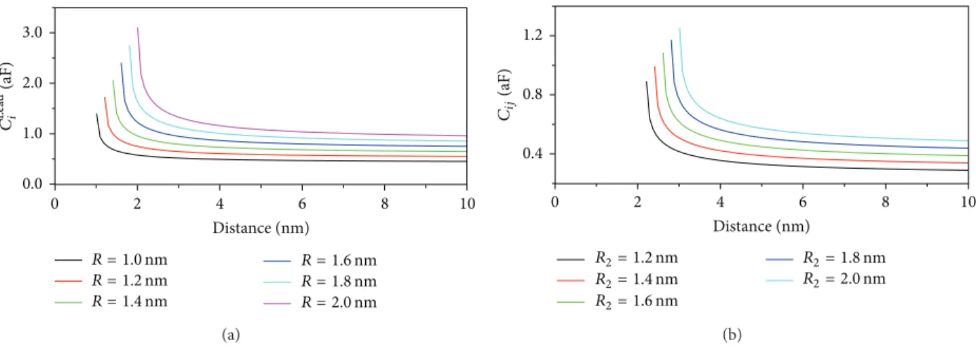
R = 1.2 nm R = 1.4 nm R = 1.6 nm R = 1.8 nm R = 2.0 nm R = 1.0 nm 0 2 4 6 8 10 Distance (nm) 3.0 2.0 1.0 C Lea d i (aF) 0.0 (a) R2= 1.2 nm R2= 1.4 nm R2= 1.6 nm R2= 1.8 nm R2= 2.0 nm 0 2 4 6 8 10 Distance (nm) 1.2 0.8 0.4 Cij (aF) (b)
Figure 3: (a) Electrode-Qd capacity (𝐶Lead
𝑖 ) for different Qds radii as a function of the distance. (b) Qd-Qd capacity (𝐶𝑖𝑗) for different𝑅2
radii; the radius of one Qd is hold at𝑅1= 1 nm. In both plots we use 𝜀𝑟= 3.9𝜀0, where𝜀0is the vacuum permittivity.
The first term of the previous equation is the electrostatic influence of the lead in which the bias voltage (𝑉𝑑𝑠) is applied; meanwhile, the second term is the electrostatic coupling with the neighbor Qd. The neighbors capacitive matrix is defined as𝑁 × 𝑁 symmetric matrix with zero in the diagonal terms. Both terms are multiplied by the inverse of the total Qd capacity.
The effects of the local potential on each Qd should be computed in the Qd DOS𝜌𝑖(𝐸) → 𝜌𝑖(𝐸 − 𝑈𝑖) shifting the position of the energy levels. This fact modifies the Qd charge and the currents. In(14)we observe that the local potential depends on the increasing charge density but at the same time the charge depends on the DOS which is modified by the local potential. These considerations impose a self-consistent solution of (5) and (14). The self-consitent solution of the system can be summarized as follows.
(1) For a given external bias voltage,(6)are solved and the nonequilibrium distribution functions (𝑛𝑖) of each Qd are obtained. The Qds charge are evaluated as𝑁𝑖= ∫ 𝜌𝑖(𝐸)𝑛𝑖(𝐸)𝑑𝐸.
(2) The local potential in each Qd is obtained using(14). (3) The DOS of the Qds is shifted according to their respective local potential𝜌𝑖(𝐸) → 𝜌𝑖(𝐸 − 𝑈𝑖). The transmission coefficients also change.
(4) Repeat until the potential of the Qds converge. Before we present in detail the code implementation, the capacitive couplings among the different parts are described. 2.3.1. Capacitive Elements. A realistic modelization of the capacitive coupling between the different parts of the systems [46] is needed, since the electron needs available states in the Qds in order to have transport and the DOS of each Qd depends on the local potential. Therefore, the position of the energy levels with the applied bias voltage plays an important role in the determination of the𝐼-𝑉 curve.
We use the analytical relationship for a sphere to conduct plane capacitance to model the capacitance between the leads and the Qd, which is
𝐶Lead 𝑖 = 4𝜋𝜀𝑟√𝑟2− 𝑅2 ∞ ∑ 𝑛=1 1 sinh(𝑛 arccosh (𝑟/𝑅)), (16) where𝜀𝑟is the permittivity of the dielectric media,𝑅 is the Qd radius, and𝑟 is the distance between the plane and the center of the Qd.
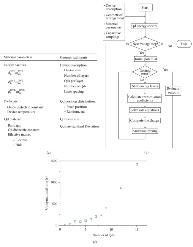
For the case of interdot capacitances (𝐶𝑖,𝑗) there is no analytical expression for the capacitance that takes into account Qds of different radii. We use the numerical method of image charges to calculate interdot capacitance between Qds of different sizes. InFigure 3we show the two capacitive terms as a function of the distance and for different Qd radii. 2.3.2. Code Implementation. Since the methodology was presented and realistic parameters have been used, putting all together, we can describe the ballistic transport through an array of Qds embedded in an insulator matrix. We have to note that the inputs for the transport code are only material parameters and the geometry of the device. A summary of the different inputs is shown inFigure 4(a).
Now, we are going to describe briefly the code implemen-tation and some compuimplemen-tational strategies that we have used in order to create the computational tool. The code is divided in 3 main parts.
(1) Input parameters: define the geometrical and the material parameters that form the device. The number of Qds is also defined. Calculate all the voltage independent parameters.
(2) SCF process: start the voltage loop. For each voltage point, the SCF process is repeated until it converges to the desired error.
(3) Output: calculate the output values.
The scheme flowchart of the code is presented inFigure 4(b). The first part of the code generates the system, the Qd
Geometrical inputs
Material parameters
Energy barriers Device description: Device area Number of layers Qds per layer Number of Qds Layer spacing Qd position distribution: ∙ Fixed position Qd mean size
Qd size standard Deviation Dielectric
Oxide dielectric constant Device temperature Qd material Band gap Qd dielectric constant Effective masses ∙ Electron ∙ Hole ∙ Random, etc. 𝜙ECBb mECBox 𝜙EVBb moxEVB 𝜙HVBb mHVBox (a) Yes No Stop Anderson mixing Compute the charge Solve rate equations Calculate transmission
coefficients Shift energy levels
Next voltage step?
Qd energy spectra Start No Yes Initial potential Evaluate outputs Desired error? ∙ Device description ∙ Geometrical arrangement ∙ Material parameters ∙ Capacitive couplings (b) 0 5 10 15 Number of Qds 1500 1000 500 0 C o m p u ta tio nal time (s) (c)
Figure 4: (a) List of the input parameters that describe the device. (b) Scheme flowchart of the self-consistent transport methodology. (c) Computational time versus number of simulated Qds. The time is referred for a single voltage point.
arrangement, and takes into account the material parame-ters needed to describe the Qds and the insulator matrix. Moreover, the capacitive couplings, the binding electron/hole energy levels, and the tunneling distances are also calculated.
For each external bias voltage point, the self-consistent methodology is used to obtain a simultaneous convergence of the local potential and the charge in each Qd. In order to accelerate the convergence of this set of equations, we have
implemented Anderson’s method [47, 48]. This procedure consists of the minimization of the “distance” between the input (𝑈in) and the output (𝑈out) potentials. The distance is
defined as
𝐷 [𝑈out, 𝑈in] = (⟨𝑈out− 𝑈in| 𝑈out− 𝑈in⟩)
1/2= ⟨𝐹 | 𝐹⟩1/2,
(17) where⟨𝑈out− 𝑈in| is a vector of the differences for each Qd.
Two “average” mixed potentials are defined for each iteration step as
𝑈in(out)⟩ = (1 − 𝛽) 𝑈in(𝑚)(out)⟩ + 𝛽 𝑈in(𝑚−1)(out)⟩ , (18)
where 𝑚 is the current iteration. The aim is to obtain the “best”𝛽 value for the current iteration which minimize the distance between these two average quantities. It reads as
𝛽 = ⟨𝐹
(𝑚)| 𝐹(𝑚)− 𝐹(𝑚−1)⟩
𝐷2[𝐹𝑚, 𝐹𝑚] . (19)
Finally, to obtain the new guess for the next iteration, we simply mix the average𝑈inand𝑈outpotentials:
𝑈(𝑚+1)⟩ = (1 − 𝛼)𝑈𝑚out⟩ + 𝛼 𝑈 𝑚
in⟩ , (20)
where𝛼 is chosen empirically. This scheme is implemented in the code as follows.
(1) Initialize the variables with the last value of the previous voltage point. For the first voltage point the variables start with zero.
(2) Calculate the solution of the Poisson equation𝑈outfor
given𝑈in.
(3) Calculate the value of𝛽.
(4) Calculate the average mixing for the input𝑈in.
(5) Calculate the average value for the output𝑈out.
(6) Do the simple mixing between the input and output potentials.
(7) Save values for the next iteration.
(8) Repeat steps (2)–(7) until the desired convergence is achieved.
Once the convergence has been achieved, the outputs can been obtained for this voltage step. In a final staged part, the outputs (Qd occupancy versus voltage, current versus voltage, and local potential versus voltage) are calculated for each voltage point and saved in a matrix structure. The process repeats until all the bias voltage steps have been done using the previous potential results as the initial guess for the next bias voltage iteration. InFigure 4(c) we show the computational time needed to obtain results for one voltage point as a function of the number of Qds. The computational time grows with the number of Qds but it is still reasonable and allows simulating large Qd arrays.
The methodology has been explained in depth to enable the interested reader to create his/her own code and repro-duce the following results. However, implementation of the code for specific devices is available (The developed code is available under agreement in contact with the author
Table 1: Parameters used in the simulation in order to describe Si Qds embedded in SiO2insulator matrix.𝑚0and𝜀0are the free electron mass and the vacuum permittivity, respectively.
𝑚∗
ECB(𝑚0) 0.40 [23,24] 𝜙1,ECB(eV) 3.1 [25,26]
𝑚∗ EVB(𝑚0) 0.30 [23] 𝜙1,HVB(eV) −4.5 [25,26] 𝑚∗ HVB(𝑚0) 0.32 [23] 𝐸gap(eV) 1.12 [25,26] 𝑚∗ Qd,CB(𝑚0) 0.33 [27] 𝜀𝑟SiO2(𝜀0) 3.9 [26,28] 𝑚∗ Qd,VB(𝑚0) 0.28 [27] 𝜀𝑟Si(𝜀0) 11.7 [26,28]
3. Application and Discussion
The above-described self-consistent transport simulator has been applied to study the ballistic electronic transport in different generic devices based on silicon Qds embedded in SiO2matrix (Si/SiO2Qds). The parameters used to describe the materials are listed inTable 1. The𝑚∗ECB,𝑚∗EVB, and𝑚∗HVB are the oxide effective masses for the different tunneling processes; the values are extracted from Lee and Hu [39]. 𝑚∗
Qd,CBand𝑚∗Qd,VBare the electron and hole Si bulk effective
masses used to obtain the binding states in the Qd. We consider that the equilibrium Fermi level is in the middle of Si 𝐸gap; confinement potentials of the Qd are𝜙1,ECBfor electrons
and 𝜙1,HVB for holes, respectively. Finally, 𝜀𝑟 is the relative permittivity of the SiO2matrix.
The electron transport takes place from the left electrode to the right electrode through the Qds. From a physical point of view, the most general transport condition is that the energy levels of the Qds (𝜖𝑖) must lie between the electrochemical potentials of the leads (𝜇𝐿 − 𝜇𝑅 = −𝑞𝑉𝑑𝑠); this condition can be summarized as𝜇𝐿 ≥ 𝜖𝑖 ≥ 𝜇𝑅. The type of transport will depend on the nature of these energy levels and electron or hole binding energy levels. Moreover, in order to have transport between the Qds, overlapping of the Qd DOS is necessary. Free states in the arriving Qd are also needed. These two conditions are directly related to the expression of the tunneling current described by(4). The transmission coefficients are also strongly dependent on the tunneling distance; therefore, some processes are more favored than others. Thus, the electronic transport plays with the transmission probabilities between the different processes and the available states.
The total net current will be the sum of the partial tunnel currents among the Qds and the right lead (electron and hole terms). This net current is going to be dependent on the position of the Qds, the tunneling distances, and the alignment of the energy levels (the local potential and the DOS of each Qd).
3.1. Single Si/SiO2Qd. Before we simulate a complete device
based on large arrays of Qds, we are going to describe a single Si/SiO2Qd in different configurations. From this small system, we will show the basis of the ballistic transport and the effects of the geometrical arrangement of the Qds in the final electrical response.
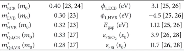
In Figure 5, we present the obtained 𝐼(𝑉) curves and the accumulated charge for a system composed of two leads separated by 5 nm and a single Si/SiO2 Qd connected to
10−13 10−11 10−9 10−7 10−5 −8 −6 −4 −2 0 2 4 6 8 Voltage (V) C u rr en t (A ) Itotal Ie− Ih+ (a) 0.1 0.0 −0.1 Acc u m u la te d charge (q ) −8 −6 −4 −2 0 2 4 6 8 Voltage (V) (b) 10−13 10−11 10−9 10−7 10−5 −8 −6 −4 −2 0 2 4 6 8 Voltage (V) C u rr en t (A ) (c) 4 2 0 −2 −4 x = 2.4 nm x = 2.3 nm x = 2.2 nm x = 2.1 nm x = 2.0 nm A cc u m u la te d charge (q ) −8 −6 −4 −2 0 2 4 6 8 Voltage (V) (d) 10−13 10−11 10−9 10−7 10−5 −8 −6 −4 −2 0 2 4 6 8 Voltage (V) C u rr en t (A ) (e) 4 2 0 −2 −4 x = 3.0 nm x = 2.9 nm x = 2.8 nm x = 2.7 nm x = 2.6 nm A cc u m u la te d charge (q ) −8 −6 −4 −2 0 2 4 6 8 Voltage (V) (f)
Figure 5: A single Si/SiO2Qd of𝑅 = 1.5 nm placed in different positions between the two leads. 𝑥 is the distance from the left lead to the center of the Qd. The separation among the leads is 5 nm. ((a)-(b))𝐼(𝑉) curve and accumulated charge for a centered Qd. The hole and electron currents are also shown. ((c)–(e))𝐼(𝑉) curves for different Qd positions and ((e)-(f)) accumulated charge in the same cases.
them placed at different positions. The position of the Qd, 𝑥, is measured from the left lead. An external bias voltage is applied to the right lead whereas the left one is kept as a reference; this means𝜇𝐿 = 0 and 𝜇𝑅 = −𝑞𝑉. Concerning the accumulate charge, it reflects the variation of the number of electrons with respect to the initial number. Therefore, if the charge is negative it implies that the system looses charge (hole accumulation). However, if the charge is positive this implies that the system increases its charge (electron accumulation).
Figure 5(a)shows the total𝐼(𝑉) curve and the hole and electron currents for a Qd connected symmetrically to both leads, which is𝑥 = 2.5 nm. Concerning the partial currents (electron and hole contributions), the electron current is the dominating term since the electron barrier (3.1 eV) is smaller than the hole barrier (4.5 eV). Besides, the opening of the discrete electron/hole conductive channels is clearly visible in the current steps at different voltages due to the position of the discrete electron/hole energy levels. Since the system is symmetrically coupled to the leads, the total current is symmetric in both polarization directions.
Regarding the accumulated charge, inFigure 5(b), the Qd remains practically uncharged. The obtained trend reflects the position of the electron and hole energy states respect to the equilibrium Fermi level and the effect of the self-charge. An electron state is the first energy level that starts to be conductive but a hole conductive channel is opened immediately being the Qd accumulated charge the difference between the electron and hole fluxes.
The𝐼(𝑉) curves and the accumulated charge are shown in Figures5(c)-5(d)and5(e)-5(f)for the nearest case to the left lead (𝑥 < 2.5) and for the right lead (𝑥 > 2.5), respectively. As can be seen, the symmetry in the total𝐼(𝑉) curve has been broken due to the different capacitive coupling among the leads [49]. Moreover, the Qd gains/loses net charge. Besides, we must note that the obtained trends for the𝑥 < 2.5 cases are complementary to the𝑥 > 2.5 cases.
When an external polarization is applied, different incoming/outgoing fluxes are created and the occupation of the states differs from the equilibrium case. Besides, the transport takes place on the energy region between𝜇𝐿 and 𝜇𝑅. Thus, only the energy states placed in this energy region can gain or lose charge. From the rate equation model, the Qd nonequilibrium distribution function in the steady state can be viewed as a balance between the two leads that strongly depends on the transmission coefficients and the occupation of the leads. Since the leads occupation is well described by the electrochemical potentials 𝜇𝐿/𝑅, the Qd energy level occupation is dominated by the highest transmission coefficient. Therefore, the lead connected to the Qd with the highest transmission coefficient dominates the Qd occupation. Since the transmission coefficients are strongly dependent on the tunneling distance, for lower voltages, the closer lead will dominate the final response. However, for larger voltages, the band bending of the wider oxide increases giving an smaller effective tunneling distance and the Qd recovers its initial charge.
3.2. Electron Transport through Si/SiO2Qds Arrays. In order
to deal with devices based on Qd arrays, we are going to
study the electron transport in a multilayer structure. This part is going to be one of the most important building blocks of the devices and, therefore, it is important to have a good characterization of it. From the experimental point of view, the superlaticce approach (SL) [50–52] allows creating these kind of structures: layers of Qds separated by insulator layers and size-controlled Qds.
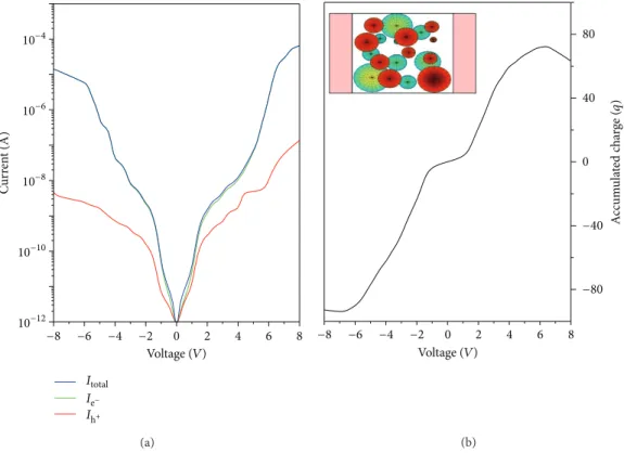
Here, we present the 𝐼(𝑉) and the total accumulated charge for a multilayer structure. The structure is formed by 2 Si Qds layers. The leads are placed perpendicular to them; therefore, the electronic transport takes place laterally. Both layers are spaced by 5 nm and the layer size is 20 nm length and 20 nm width. We simulate 10 randomly distributed Qds per layer and for the Qds radii we use a normal distribution with 1.75 nm mean value and 0.3 nm standard deviation. A top view scheme of the system is shown in the inset of
Figure 6(b).
InFigure 6(a), the total𝐼(𝑉) curve and the electron and hole currents terms are shown. From the𝐼(𝑉) curves, two different regimes are obtained: for low and medium voltage ranges, the current reflects the discrete nature of the Qds energy spectra. However, for the largest voltages, the contin-uous part of the Qd DOS begins to be conductive and the current increases in a continuous form loosing its step-like shape. Concerning the electron/hole current components, the electron term dominates since its potential barrier is lower than the hole one. Moreover, the stepping behavior is still present in the current reflecting the aperture of the different conductive channels. In this case, the transport involves several tunneling processes between the Qds. Therefore, the energy level alignment is necessary. However, the negative differential resistance (NDR) is not clearly visible since there are many electron/hole pathways and the sum of the different conduction channels masks this effect [22].
Regarding the accumulated charge plotted inFigure 6(b), it is the total sum of the accumulated charge in each Qd (∑𝑖Δ𝑁𝑖 where 𝑖 = 1 ⋅ ⋅ ⋅ 20). The geometrical disposition of the Qds strongly affects the final response of the system as we have shown in the previous section. For this system, since there are many electronic conduction channels and a complex capacitive interaction between the Qds, it is hard to explain clearly the accumulated charge trend. Reflecting that, the geometrical disposition of the Qds influences directly the final response of the system.
4. Conclusions
The high efficiency concepts of the next generation of Qds based devices pose new requirements on models for the theoretical description of their transport properties. An intuitive theoretical framework suitable for this purpose is available in the noncoherent rate equations. This approach provides a simple and transparent method to describe the electron transport. Using the Transfer Hamiltonian approach to describe the tunneling current terms in ballistic regime, the rate equations can be used in order to obtain the nonequilibrium distribution functions in each Qd. The effect of self-charge has been taken into account solving the Poisson equation with the appropriate boundary conditions for each
−8 −6 −4 −2 0 2 4 6 8 Voltage (V) 10−12 10−10 10−8 10−6 10−4 C u rr en t (A ) Itotal Ie− Ih+ (a) −8 −6 −4 −2 0 2 4 6 8 Voltage (V) 80 40 0 −80 −40 A cc u m u la te d charge (q ) (b)
Figure 6: (a) Obtained𝐼(𝑉) curves (electron/hole and total currents) for two layers of 10 Si/SiO2Qds. The system arrangement is described in the text. The Qds radius distribution is also shown in the inset. (b) Total accumulated charge (∑𝑖Δ𝑁𝑖where𝑖 = 1 ⋅ ⋅ ⋅ 20) of the structure
as a function of the external bias voltage. In the inset, a top view of the system is presented.
Qd that involve the capacity coupling between the different parts of the system and the accumulated charge in each Qd. As expected, the calculation of the local potential inside each Qd is one of the most critical points, since the 𝐼-𝑉 curves depend on the position of the energy level. Due to the simplicity of the model, this can be easily extended to analyze arbitrary large arrays of Qds of interest in technological applications creating a powerful and useful tool that enables to design new concept devices based on Qd properties.
In order to simulate devices as realistic as possible, suitable expressions for the transmission coefficients, the energy level positions and the capacitive coupling have been used. These parameters can be described using basic material properties and geometrical representations of the system. Moreover, the hole currents have been taken into account, obtaining a complete description of the electron transport in the structure.
Finally, the proposed formalism has been used to describe, using realistic material parameters, the electrical response of a single Si/SiO2Qd. Moreover, a bilayer structure has also been simulated. This structure composes the basic building block for future devices based on Qds and demon-strates the practicability of the here presented approach.
Conflict of Interests
The authors declare that there is no conflict of interests regarding the publication of this paper.
Acknowledgments
S. Illera is supported by the FI programme of the Generalitat de Catalunya. A. Cirera acknowledges support from ICREA academia program. The authors thankfully acknowledge the computer resources, technical expertise, and assistance provided by the Barcelona Supercomputing Center (Centro Nacional de Supercomputaci´on). The research leading to these results has received funding from the European Com-munity’s Seventh Framework Programme (FP7/2007-2013) under Grant Agreement no. 245977.
References
[1] T. Ando, A. B. Fowler, and F. Stern, “Electronic properties of two-dimensional systems,” Reviews of Modern Physics, vol. 54, no. 2, pp. 437–672, 1982.
[2] U. Meirav and E. B. Foxman, “Single-electron phenomena in semiconductors,” Semiconductor Science and Technology, vol. 11, no. 3, pp. 255–284, 1996.
[3] S. Tiwari, F. Rana, K. Chan, L. Shi, and H. Hanafi, “Single charge and confinement effects in nano-crystal memories,” Applied Physics Letters, vol. 69, no. 9, pp. 1232–1234, 1996.
[4] D. J. Lockwood, Light Emission in Silicon: From Physics to Devices, Semiconductors and Semimetals, Academic Press, San Diego, Calif, USA, 1998.
[5] R. C. Ashoori, “Electrons in artificial atoms,” Nature, vol. 379, pp. 413–419, 1996.
[6] D. H. Cobden, M. Bockrath, P. L. McEuen, A. G. Rinzler, and R. E. Smalley, “Spin splitting and even-odd effects in carbon nanotubes,” Physical Review Letters, vol. 81, no. 3, pp. 681–684, 1998.
[7] J. B. Barner and S. T. Ruggiero, “Observation of the incremental charging of Ag particles by single electrons,” Physical Review Letters, vol. 59, no. 7, pp. 807–810, 1987.
[8] J. Weis, R. J. Haug, K. V. Klitzing, and K. Ploog, “Competing channels in single-electron tunneling through a quantum dot,” Physical Review Letters, vol. 71, no. 24, pp. 4019–4022, 1993. [9] S. D. Wang, Z. Z. Sun, N. Cue, H. Q. Xu, and X. R. Wang,
“Negative differential capacitance of quantum dots,” Physical Review B, vol. 65, no. 12, Article ID 125307, 2002.
[10] W. G. van der Wiel, S. D. Franceschi, T. Fujisawa, J. M. Elzerman, S. Tarucha, and L. P. Kouwenhoven, “The Kondo effect in the unitary limit,” Science, vol. 289, no. 5487, pp. 2105–2108, 2000. [11] R. J. Haug, J. M. Hong, and K. Y. Lee, “Electron transport
through one quantum dot and through a string of quantum dots,” Surface Science, vol. 263, no. 1–3, pp. 415–418, 1992. [12] N. C. van der Vaart, S. F. Godijn, Y. V. Nazarov et al., “Resonant
tunneling through two discrete energy states,” Physical Review Letters, vol. 74, no. 23, pp. 4702–4705, 1995.
[13] F. R. Waugh, M. J. Berry, D. J. Mar, R. M. Westervelt, K. L. Campman, and A. C. Gossard, “Single-electron charging in double and triple quantum dots with tunable coupling,” Physical Review Letters, vol. 75, no. 4, pp. 705–708, 1995.
[14] B. H. Choi, S. W. Hwang, I. G. Kim, H. C. Shin, Y. Kim, and E. K. Kim, “Fabrication and room-temperature characterization of a silicon self-assembled quantum-dot transistor,” Applied Physics Letters, vol. 73, no. 21, pp. 3129–3131, 1998.
[15] S. Tiwari, F. Rana, H. Hanafi, A. Hartstein, E. F. Crabb´e, and K. Chan, “A silicon nanocrystals based memory,” Applied Physics Letters, vol. 68, no. 10, pp. 1377–1379, 1996.
[16] R. Ohba, N. Sugiyama, K. Uchida, J. Koga, and A. Toriumi, “Non-volatile Si quantum memory with self-aligned doubly-stacked dots,” in Proceedings of the International Electron Devices Meeting. Technical Digest (IEDM ’00), pp. 313–316, San Francisco, Calif, USA, December 2000.
[17] W. Gong, Y. Zheng, Y. Liu, and T. L¨u, “A Feynman path analysis of the Fano effect in electronic transport through a parallel double quantum dot structure,” Physica E: Low-Dimensional Systems and Nanostructures, vol. 40, no. 3, pp. 618–626, 2008. [18] A. L. Yeyati, A. Mart´ın-Rodero, and F. Flores, “Electron
corre-lation resonances in the transport through a single quantum level,” Physical Review Letters, vol. 71, no. 18, pp. 2991–2994, 1993.
[19] Y. Meir and N. S. Wingreen, “Landauer formula for the current through an interacting electron region,” Physical Review Letters, vol. 68, no. 16, pp. 2512–2515, 1992.
[20] S. A. Gurvitz, “Rate equations for quantum transport in multidot systems,” Physical Review B—Condensed Matter and Materials Physics, vol. 57, no. 11, pp. 6602–6611, 1998.
[21] S. Illera, J. D. Prades, A. Cirera, and A. Cornet, “Transport in quantum dot stacks using the transfer Hamiltonian method in self-consistent field regime,” Europhysics Letters, vol. 98, no. 1, Article ID 17003, 2012.
[22] S. Illera, N. Garcia-Castello, J. D. Prades, and A. Cirera, “A transfer Hamiltonian approach for an arbitrary quantum dot array in the self-consistent field regime,” Journal of Applied Physics, vol. 112, no. 9, Article ID 093701, 2012.
[23] W.-C. Lee and C. Hu, “Modeling CMOS tunneling currents through ultrathin gate oxide due to conduction- and valence-band electron and hole tunneling,” IEEE Transactions on Elec-tron Devices, vol. 48, no. 7, pp. 1366–1373, 2001.
[24] Y.-C. Yeo, T.-J. King, and C. Hu, “MOSFET gate leakage modeling and selection guide for alternative gate dielectrics based on leakage considerations,” IEEE Transactions on Electron Devices, vol. 50, no. 4, pp. 1027–1035, 2003.
[25] G. Conibeer, M. Green, R. Corkish et al., “Silicon nanostruc-tures for third generation photovoltaic solar cells,” Thin Solid Films, vol. 511-512, pp. 654–662, 2006.
[26] S. Okhonin, P. Fazan, G. Guegan, S. Deleonibus, and F. Martin, “Two-band tunneling currents in metal-oxide-semiconductor capacitors at the transition from direct to Fowler-Nordheim tunneling regime,” Applied Physics Letters, vol. 74, no. 6, pp. 842–843, 1999.
[27] S. M. Sze, Semiconductor Devices, Physics and Technology, John Wiley & Sons, Hoboken, NJ, USA, 2001.
[28] J. M. Ram´ırez, Y. Berenc´en, L. L´opez-Conesa, J. M. Rebled, F. Peir´o, and B. Garrido, “Carrier transport and electrolu-minescence efficiency of erbium-doped silicon nanocrystal superlattices,” Applied Physics Letters, vol. 103, no. 8, Article ID 081102, 2013.
[29] M. A. Kastner, “The single-electron transistor,” Reviews of Modern Physics, vol. 64, no. 3, pp. 849–858, 1992.
[30] H. I. Hanafi, S. Tiwari, and I. Khan, “Fast and long retention-time nano-crystal memory,” IEEE Transactions on Electron Devices, vol. 43, no. 9, pp. 1553–1558, 1996.
[31] O. Jambois, J. Carreras, A. P´erez-Rodr´ıguez et al., “Field effect white and tunable electroluminescence from ion beam synthesized Si- and C-rich SiO2layers,” Applied Physics Letters, vol. 91, no. 21, Article ID 211105, 2007.
[32] A. J. Nozik, “Quantum dot solar cells,” Physica E: Low-Dimensional Systems and Nanostructures, vol. 14, no. 1-2, pp. 115–120, 2002.
[33] H. Grabert and M. H. Devoret, Single Charge Tunneling: Coulomb Blockade Phenomena in Nanstructures, Plenum Press, 1992.
[34] D. K. Ferry and S. M. Goodnick, Transport in Nanostructures, Cambridge University Press, Cambridge, UK, 2009.
[35] M. C. Payne, “Transfer Hamiltonian description of resonant tunnelling,” Journal of Physics C: Solid State Physics, vol. 19, no. 8, pp. 1145–1155, 1986.
[36] J. J. Sakurai, Modern Quantum Mechanics, Addison-Wesley, 1994.
[37] J. S´ee, P. Dollfus, S. Galdin, and P. Hesto, “From wave-functions to current-voltage characteristics: overview of a Coulomb blockade device simulator using fundamental physical param-eters,” Journal of Computational Electronics, vol. 5, no. 1, pp. 35– 48, 2006.
[38] S. Datta, Electronic Transport in Mesoscopic Systems, Cambridge University Press, Cambridge, UK, 1995.
[39] W.-C. Lee and C. Hu, “Modeling CMOS tunneling currents through ultrathin gate oxide due to conduction-and valence-band electron and hole tunneling,” IEEE Transactions on Elec-tron Devices, vol. 48, no. 7, pp. 1366–1373, 2001.
[40] V. A. Ukraintsev, “Data evaluation technique for electron-tunneling spectroscopy,” Physical Review B, vol. 53, Article ID 11176, 1996.
[41] J. H. Davies, The Physics of Low Dimensiobal Semiconductors, Cambridge University Press, 1998.
[42] I. P. Batra, “From uncertainty to certainty in quantum conduc-tance of nanowires,” Solid State Communications, vol. 124, no. 12, pp. 463–467, 2002.
[43] N. Garcia-Castello, S. Illera, R. Guerra, J. D. Prades, S. Ossicini, and A. Cirera, “Silicon quantum dots embedded in a SiO2 matrix: from structural study to carrier transport properties,” Physical Review B—Condensed Matter and Materials Physics, vol. 88, no. 7, Article ID 075322, 2013.
[44] S. Datta, Quantum Transport: Atom to Transistor, Cambridge University Press, 2005.
[45] S. Datta, “Electrical resistance: an atomistic view,” Nanotechnol-ogy, vol. 15, no. 7, pp. S433–S451, 2004.
[46] J. Carreras, O. Jambois, S. Lombardo, and B. Garrido, “Quantum dot networks in dielectric media: from compact modeling of transport to the origin of field effect luminescence,” Nanotech-nology, vol. 20, no. 15, Article ID 155201, 2009.
[47] D. D. Johnson, “Modified Broyden’s method for accelerating convergence in self-consistent calculations,” Physical Review B, vol. 38, no. 18, pp. 12807–12813, 1988.
[48] D. G. Anderson, “Iterative procedures for nonlinear integral equations,” Journal of the ACM, vol. 12, no. 4, pp. 547–560, 1965. [49] S. Illera, J. D. Prades, A. Cirera, and A. Cornet, “Transport in quantum dot stacks using the transfer Hamiltonian method in self-consistent field regime,” EPL, vol. 98, no. 1, Article ID 17003, 2012.
[50] M. Zacharias, J. Heitmann, R. Scholz, U. Kahler, M. Schmidt, and J. Bl¨asing, “Size-controlled highly luminescent silicon nanocrystals: a SiO/SiO2superlattice approach,” Applied Physics Letters, vol. 80, article 661, 2002.
[51] F. Iacona, G. Franz`o, and C. Spinella, “Correlation between luminescence and structural properties of Si nanocrystals,” Journal of Applied Physics, vol. 87, no. 3, pp. 1295–1303, 2000. [52] V. A. Belyakov, V. A. Burdov, R. Lockwood, and A. Meldrum,
“Silicon nanocrystals: fundamental theory and implications for stimulated emission,” Advances in Optical Technologies, vol. 2008, Article ID 279502, 32 pages, 2008.