DOCTORAL SCHOOL UNIVERSITA’ MEDITERRANEA DI REGGIO CALABRIA DIPARTIMENTO DI INGEGNERIA DELL’INFORMAZIONE, DELLE INFRASTRUTTURE E DELL’ENERGIA SOSTENIBILE (DIIES) PHD IN INFORMATION ENGINEERING
S.S.D. FIS/01 XXXI CICLO
ETHANOL-CVD GROWTH OF LARGE SINGLE-CRYSTAL
GRAPHENE AND GRAPHENE-BASED DERIVATIVE FOR
PHOTOVOLTAIC APPLICATIONS
CANDIDATE AndreaG
NISCI ADVISOR Dr. GiulianaF
AGGIO COORDINATORP
rof. TommasoI
SERNIAFinito di stampare nel mese di Febbraio 2019
Edizione
Quaderno N. 41
Collana Quaderni del Dottorato di Ricerca in
Ingegneria dell’Informazione
Curatore Prof. Tommaso Isernia
ISBN 978-88-99352-32-5
Università degli Studi Mediterranea di Reggio Calabria
A
NDREAG
NISCIETHANOL-CVD GROWTH OF LARGE SINGLE-CRYSTAL
GRAPHENE AND GRAPHENE-BASED DERIVATIVE FOR
PHOTOVOLTAIC APPLICATIONS
The Teaching Staff of the PhD course in
INFORMATION ENGINEERING
consists of:
Tommaso ISERNIA (coordinator) Giovanni ANGIULLI Pier Luigi ANTONUCCI Giuseppe ARANITI Francesco BUCCAFURRI Rosario CARBONE Riccardo CAROTENUTO Salvatore COCO Maria Antonia COTRONEI Claudio DE CAPUA Francesco DELLA CORTE Aimè LAY EKUAKILLE Giuliana FAGGIO Fabio FILIANOTI Patrizia FRONTERA Sofia GIUFFRE' Antonio IERA Gianluca LAX Giacomo MESSINA Antonella MOLINARO Andrea Francesco MORABITO Rosario MORELLO Fortunato PEZZIMENTI Sandro RAO Domenico ROSACI Giuseppe RUGGERI Maria Teresa RUSSO Valerio SCORDAMAGLIA Domenico URSINO And also: Antoine BERTHET Dominique DALLET Lubomir DOBOS Lorenzo CROCCO Ivo RENDINA Groza VOICU
…to my dearly loved sister, Daniela
“To Infinity and Beyond!”
Buzz Lightyear of Star Command
Contents
CONTENTS ... I LIST OF FIGURES ... III
INTRODUCTION ... 1
GRAPHENE ... 5
1.1 INTRODUCTION ... 5
1.2 THE PHYSICS OF GRAPHENE ... 6
1.2.1 CARBON HYBRIDIZATION OF GRAPHENE ... 6
1.2.2 GRAPHENE CRYSTAL STRUCTURE ... 8
1.2.3 THE BAND STRUCTURE OF GRAPHENE ... 10
1.3GRAPHENE PROPERTIES ... 14
1.3.1ELECTRONIC TRANSPORT PROPERTIES OF GRAPHENE ... 14
1.3.2SCATTERING IN GRAPHENE ... 15
1.3.3.OPTOELECTRONIC PROPERTIES OF GRAPHENE ... 16
1.3.4THERMAL CONDUCTIVITY IN GRAPHENE ... 18
1.3.5PHYSICAL PROPERTIES OF GRAPHENE ... 19
1.3.6CHEMICAL AND SURFACE PROPERTIES ... 19
1.4 GRAPHENE SYNTHESIS ... 20
1.4.1 MECHANICAL EXFOLIATION ... 21
1.4.2 LIQUID PHASE EXFOLIATION ... 22
1.4.3 EPITAXIAL GROWTH ON SIC ... 23
1.4.4 CHEMICAL VAPOUR DEPOSITION (CVD) ... 25
1.4.5 OTHER GROWTH METHODS ... 29
1.5 TRANSFER OF CVDGRAPHENE ... 30
CHARACTERIZATION TECHNIQUES ... 33
2.1 INTRODUCTION ... 33
2.2 OPTICAL MICROSCOPY ... 34
2.3 SCANNING ELECTRON MICROSCOPY (SEM) ... 35
2.4 MICRORAMAN SPECTROSCOPY ... 38
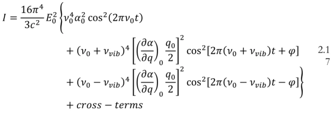
2.4.1 PRINCIPLES OF RAMAN SPECTROSCOPY ... 39
2.4.2 RAMAN FEATURES OF GRAPHENE ... 47
2.5 ATOMIC FORCE MICROSCOPY (AFM) ... 51
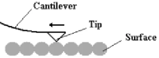
2.5.1 PROBING FORCES WITH A CANTILEVER... 54
CANTILEVER MOTION DETECTION ... 55
NOISE CONSIDERATIONS AND OPTIMAL RESOLUTION ... 56
2.5.2 MODE OF OPERATION ... 57
CONTACT MODE AFM(C-AFM) ... 57
NON-CONTACT MODE AFM(NC-AFM) ... 58
ATTRACTIVE AND REPULSIVE FORCES ... 59
TAPPING MODE AFM ... 61
AMPLITUDE MODULATION AFM ... 62
FREQUENCY MODULATION AFM ... 63
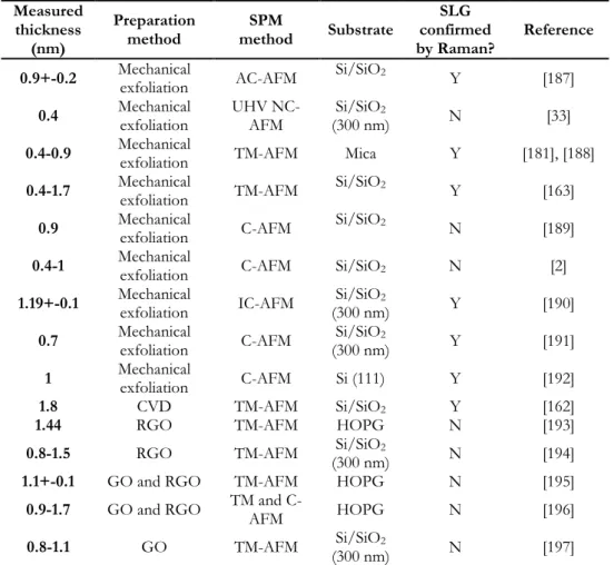
2.5.3 ANOMALIES IN THICKNESS MEASUREMENTS OF GRAPHENE BY TM-AFM ... 65
2.5.4 SIMULTANEOUS AFM-RAMAN ... 70
2.6 KELVIN PROBE FORCE MICROSCOPY (KPFM) ... 71
2.7 GRAPHENE FIELD EFFECT TRANSISTOR (GFET) FOR MOBILITY MEASUREMENTS .... 73
2.8 SOLAR CELL CHARACTERIZATION ... 76
2.8.1 EXTERNAL QUANTUM EFFICIENCY (EQE) ... 76
2.8.2 PHOTOVOLTAIC PARAMETERS ... 77
3.5 LARGE GRAPHENE DOMAINS GROWTH ... 94
3.5.1 NUCLEATION DENSITY REDUCTION ... 94
3.5.2 EFFECT OF ETHANOL FLOW:TOWARDS LARGE GRAPHENE GRAINS ... 97
3.5.3 HIGH-TEMPERATURE GROWTH OF LARGE GRAPHENE GRAINS ... 100
3.5.4 ELECTRICAL PROPERTIES OF SUB-MM GRAPHENE GRAINS BY ETHANOL -CVD ... 102
GRAPHENE BASED DERIVATIVE INTERLAYER IN GRAPHENE ON SILICON SCHOTTKY BARRIER SOLAR CELLS ... 105
4.1 INTRODUCTION ... 105
4.2 THE SCHOTTKY JUNCTION ... 107
4.2.1 THE SCHOTTKY BARRIER ... 108
4.2.2 THERMIONIC EMISSION AND I–V CHARACTERISTIC ... 114
4.2.3 ANALYSIS OF I-V CHARACTERISTIC ... 119
4.3 GRAPHENE ON SILICON SCHOTTKY JUNCTION WITH GBD INTERLAYER ... 120
4.3.1 GRAPHENE ON SILICON SCHOTTKY JUNCTION ... 120
4.3.2 THE INTERFACE ENGINEERING IN SCHOTTKY JUNCTION ... 125
4.3.3 DEVICE REALIZATION... 126
SUBSTRATE PREPARATION ... 126
FILMS GROWTH AND TRANSFER ON SUBSTRATE ... 129
4.3.4 GBD AND FEW LAYER GRAPHENE CHARACTERIZATION ... 132
4.4 SOLAR CELL CHARACTERIZATION ... 135
4.4.1 ELECTRICAL CHARACTERIZATION ... 135 4.4.2 PHOTOVOLTAIC CHARACTERIZATION ... 138 4.5 DOPING TREATMENT ... 139 CONCLUSIONS ... 144 REFERENCES ... 147 LIST OF PUBLICATIONS... 187 ACKNOWLEDGMENTS ... 189
List of Figures
Figure 1.1. The carbon family and the considered material dimensionality. (a) Diamond (3D) (b) Graphite (3D) (c) Fullerenes (0D) (d) Nanotube (1D) (e) Graphene (2D). ... 6 Figure 1.2. The orbital evolution from a ground state energy carbon atom to
a sp2 hybridised graphene atom. ... 8 Figure 1.3. (a) The honeycomb lattice of graphene showing the two sublattices
marked A and B [7]. (b) Lattice structure of graphene showing the two sublattices marked A and B; a1 and a2 the lattice unit vectors; 𝛿𝑖 i=1, 2, 3 the nearest neighbor vectors [6]. ... 9 Figure 1.4. First Brillouin zone of graphene with the reciprocal lattice vectors
defined as b1 and b2. High symmetry k-points are labelled as Γ, M, K and K’ [6]. ... 10 Figure 1.5. Band structure of graphene. In the vicinity of the Dirac points at
the two nonequivalent corners K and K′ of the hexagonal Brillouin zone, the dispersion relation is linear and hence locally equivalent to a Dirac cone [8]. The energy dispersion is a function of the wavevector components kx and ky, as obtained from Eq. 1.3. Valence (𝜋) and conduction bands (𝜋 ∗) are seen touching at the Fermi level at the K and K’ points with a linear conical relation among them. ... 12 Figure 1.6. (a)Calculated density of states of graphene. Close to the Fermi
level, the density of states ρ(ε), is linear with respect to the energy [6]. (b) Ambipolar transport characteristic of graphene. Field induced by gate voltage, Vg can control concentration and polarity of charge carriers. Positive (negative) gate voltage increases Fermi level increasing carrier concentration of holes (electrons) [11] ... 15 Figure 1.7. Scan profile showing the intensity of transmitted white light
through air, single layer and bilayer graphene respectively [35]. ... 17 Figure 1.8. (a) Transmittance for different transparent conductors and (b)
thickness dependence of the sheet resistance [10]. ... 18 Figure 1.9. Graphene quality vs mass production cost of different graphene
fabrication methods [68]. ... 21 Figure 1.10. (a) Scotch tape mechanical exfoliation [70], (b) Exfoliated
graphene on 300 nm thick SiO2, the number of layers increases with flake contrast, the number of layers are labelled, image adapted from [71]. ... 22 Figure 1.11. Liquid phase exfoliation technique [70]. ... 23 Figure 1.12. Growth on SiC. Gold and grey spheres represent Si and C atoms,
respectively [70]. ... 24 Figure 1.13. Schematic representation of graphene mechanism growth (a)
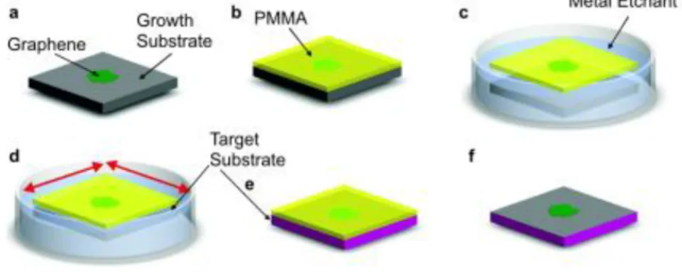
parameters: temperature, pressure and composition/flow rate for graphene growth by methane (CH4) in hydrogen (H2) flow [54]. ... 29 Figure 1.15. The wet PMMA support layer transfer process. a) Graphene
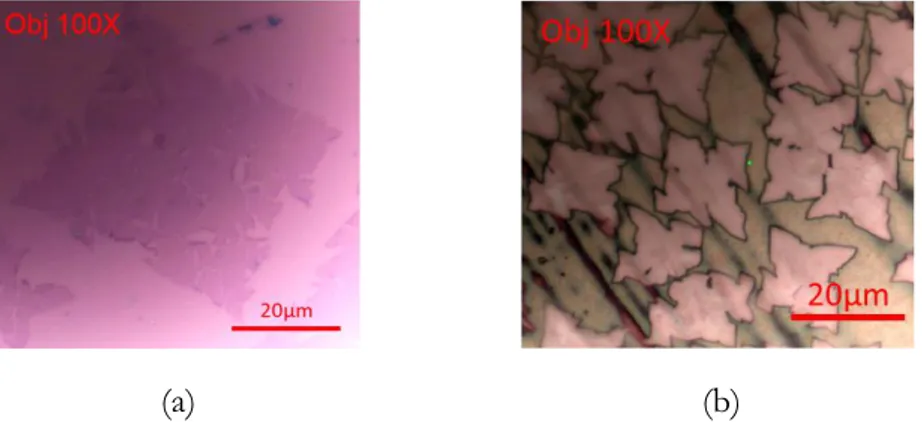
grown via CVD on metal substrate. b) PMMA is spin coated onto the graphene surface. c) The metal growth substrate is etched away. d) The target substrate is used to scoop the graphene/PMMA sample out. e) The graphene/PMMA is allowed to dry to the target substrate surface. f) The PMMA is removed with a solvent or annealing [67]. ... 31 Figure 2.1. Optical image of graphene (a) on Si/SiO2 and (b) on copper
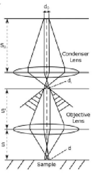
substrates. ... 35 Figure 2.2. Schematic diagram of ray traces in a typical SEM, ray divergence is
exaggerated for clarity. ... 36 Figure 2.3. (a) Interaction of Radiation-matter interaction processes:
backscattered electrons, secondary electrons, X-rays and Auger electrons and their creation mechanisms; (b) Schematic diagram of the interaction volume for electrons incident on a material. The penetration of electrons to different depths produces different imaging signals. Adapted from references [127].- ... 37 Figure 2.4. SEM micrographs of graphene on copper substrate: single and
multilayer graphene on copper. Scale bar represents 20µm [129]. ... 38 Figure 2.5. Raman spectrum of carbon tetrachloride showing Rayleigh, Stokes
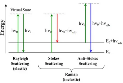
and anti-Stokes Raman bands. ... 41 Figure 2.6. Schematic representation of quantum energy transitions for
Rayleigh and Raman scattering. ... 42 Figure 2.7. Diatomic linear lattice with M1 and M2 atoms mass and lattice
spacing 2a. ... 44 Figure 2.8. Dispersion curve in biatomic crystal. Optical and acoustical
branches are shown. ... 45 Figure 2.9. Phonon dispersion relation of graphene showing the iLO, iTO,
oTO, iLA, iTA and oTA phonon branches [136]. ... 46 Figure 2.10. Role of the electron dispersion (Dirac cones, shown by solid black
lines) in Raman scattering: (a) intravalley one-phonon G peak, (b) defect-assisted intravalley one-phonon D peak, (c) intravalley two-phonon 2D peak, (d) defect assisted intervalley one-two-phonon D’ peak, (e) intervalley two-phonon 2D’ peak. Vertical solid arrows represent interband transitions accompanied by photon absorption (upward arrows) or emission (downward arrows) [140]. ... 48 Figure 2.11 Carbon motions in the G modes namely E2g and D modes namely
A1g [134]... 48 Figure 2.12. Typical Raman spectrum of graphene showing the main Raman
features, the D, G and 2D bands. ... 49 Figure 2.13. Sketch of an AFM probe showing the tip’s radius of curvature rc ... 53 Figure 2.14. AFM image of graphene film: (a) image with artefacts due to
graphene film region after measurement post-processing. In (b) the artefact due to the tip are eliminated and tears in the film are visible. ... 54 Figure 2.15. Diagram of a piezoelectric actuator exciting a cantilever, the
oscillatory motion of the cantilever is indicated... 55 Figure 2.16. Sketch the laser beam deflecting onto the quadrant photodiode. ... 56 Figure 2.17. Diagram of a contact mode AFM, the cantilever scans across the
sample whilst in direct contact with the sample. ... 57 Figure 2.18. Resonance curve for a single harmonic oscillator (solid line) and
under the influence of attractive and repulsive forces (dashed lines), A = oscillation amplitude. ... 58 Figure 2.19. Sketch of the force exerted on the tip of the AFM cantilever by
the surface, 𝐹𝑡𝑠, versus tip-sample separation distance, z, illustrating the repulsive and attractive regimes. ... 60 Figure 2.20. Sketch of tip oscillation in tapping-mode AFM. ... 61 Figure 2.21. Schematic illustration of non-contact AFM operation mode: (a)
Amplitude modulation mode and (b) Frequency modulation mode. Both AM and FM modes maintain constant tip–sample separation. AM mode uses oscillation amplitude changes as a feedback signal while FM mode uses frequency changes as feedback signal [160]. ... 65 Figure 2.22. Typical measured thickness of graphene as a function of RH. The
RH range is divided into three approximate sections: Low, Middle, and High RH [161]. ... 68 Figure 2.23. Structure of exfoliated FLG trapping the water adlayer on the
oxide substrate. Figure not shown to scale [161]. ... 69 Figure 2.24. Schematic mechanism of improving AFM imaging accuracy with
increasing peak force set point. As the pressure applied increases from (a) low to (b) medium to (c) high the AFM tip is able to disrupt the underlying buffer layer and subsequently measure a more accurate value for graphene height [170]. ... 69 Figure 2.25. (a) AFM and Raman instrumentation Schematic of AIST-NT
SPM AFM integrated with LabRamHR Evolution HORIBA Scientific Raman system allowing for the capture of simultaneous AFM-Raman. (b) The Raman laser (red shaded area) and AFM probe (blue) are both focused onto the same area of the sample and held in a fixed position. The z position of the stage is controlled by phase feedback from the probe, the stage is then moved in the x-y direction when scanning the sample. ... 70 Figure 2.26. Electronic energy levels of the sample and AFM tip for three
cases: (a) tip and sample are separated by distance d with no electrical contact, (b) tip and sample are in electrical contact, and (c) external bias (𝑉𝑑𝑐) is applied between tip and sample to nullify the CPD and,
therefore, the tip–sample electrical force. 𝐸𝑣 is the vacuum energy
level. 𝐸𝑓𝑠 and 𝐸𝑓𝑡 are Fermi energy levels of the sample and tip,
respectively. ... 72 Figure 2.27. Schematic cross section of a GFET [207]. ... 73 Figure 2.28. Ideal drain current versus gate voltage. ... 74 Figure 2.29. FET transfer characteristics showing 𝐼𝐷 (on a logarithmic scale
parameters. ... 77 Figure 2.31. The effects of series and shunt resistance on the J-V curve.
Optimal values are Rseries = 0 ohm cm2 and Rshunt = ∞ ohm cm2. ... 80 Figure 3.1. Scheme of CVD apparatus at ENEA. ... 84 Figure 3.2. Temperature-time profile during a typical growth. (I) Insertion in
the chamber, (II) evacuation and setting of the gas flows for annealing (Ar, H2), (III) insertion in the furnace hot zone and annealing, (IV) growth, (V) extraction from the hot zone and rapid cooling under Ar, (VI) filling with Ar and extraction from the chamber. Adapted from [227]. ... 86 Figure 3.3. 10X optical image of cyclododecane diluted in hexane (a) 20mg/ml
and (b) 200mg/ml spin coated at 1000rpm for 40s. ... 88 Figure 3.4. Scheme of cyclododecane transfer method process of graphene,
from Cu native substrate to Si/SiO2 substrate. ... 89 Figure 3.5. (a) Monolayer graphene films and (b) graphene islands transferred
with different concentration 0f 40%, 44% and 50% of CDD in hexane. ... 89 Figure 3.6. (a) and (b) AFM characterization of monolayer graphene film and
graphene islands, respectively, (c) and (d) Raman maps of 𝐼𝐷/𝐼𝐺 and
𝐼2𝐷/𝐼𝐺 ratios of monolayer graphene film and graphene islands,
respectively. ... 90 Figure 3.7. Schematic representation of reduction of nucleation density and
increase of crystallinity. ... 91 Figure 3.8. Raman spectra of graphene samples grown in the conditions of
Table 3.1; the graphene was grown in different conditions (Temperature, growth time, pressure, flow of ethanol) [251]. ... 92 Figure 3.9. Graphene grown at 1070°C and 65 Pa for 15 s with (a-c) Qeth =
0.1 sccm and (d-f) Qeth = 1.5×10⁻² sccm with g) averaged Raman spectra. (a,d) SEM micrographs of the as-grown graphene on the Cu substrates. (b,c) Raman mapping images (50 x 50 µm in size, 0.5 µm resolution) for AD/AG and I2D/IG after transfer on SiO2/Si. The blue arrow indicates tear caused by transfer. (e,f) Raman mapping images (17 x 17 µm in size, 0.25 µm resolution) for AD/AG and I2D/IG of graphene islands after transfer on SiO2/Si. The sample is composed of isolated monolayer graphene grains of 1 - 3 µm with smaller disorder level [251]. ... 93 Figure 3.10. (a) AFM image of the graphene grains on copper foil facets (t =
15 s, T = 1070 °C, P = 65 Pa, and Qeth = 1.5×10⁻² sccm). (b) Higher resolution AFM image of a single grain on Cu. Some grains show hexagonal shape with rounded corners. c) AFM image after transfer on SiO2/Si. (d) Height profile from (c) shows a step of 0.8 nm [251]. ... 94 Figure 3.11. Nucleation density of graphene grown on Cu substrate with
different pre-oxidation (250°C in air) time (tOX) ranging from 0 to 150 min. (a-e) Optical microscopy of the graphene grown on Cu in
the various cases. (f) Nucleation density trend vs pre-oxidation time. Adapted by [251]. ... 95 Figure 3.12. (a-c) Nucleation density of graphene grown on pre-oxidized Cu
substrate (250°C in air for 150min) with different pre-growth Ar annealing times (tann). Isolated grains grew only with 1 min Ar annealing, while in the other cases continuous films grew. Adapted by [251]. ... 96 Figure 3.13. (a) AFM image of pre-oxidized Cu foil, (b) the effect of oxygen
on copper. Reprinted from [256]. ... 97 Figure 3.14. Optical images of graphene (30 min, 1000° C, 130 Pa) grown on
pre-oxidized Cu foil with (a) 1.5×10⁻² sccm and (b) 1.5×10⁻³ sccm of ethanol. (c) The corresponding Raman spectra. [251] ... 98 Figure 3.15. Analysis of a 50-μm grain (sample P2) after transfer onto Si/SiO2.
(a) Optical micrograph of the grain, (b) AFM topography image with thickness line profile of ~ 1 nm. The value is larger than the inter-plane spacing of graphite (0.335 nm) due to intercalated molecules and to the interaction forces between graphene-substrate-tip, as found for CVD-graphene in similar experimental and environmental (relative humidity) conditions [161]–[163]. Raman mapping images of (b) 𝐴𝐷/𝐴𝐺 and (c) 𝐼2𝐷/𝐼𝐺 peak ratio (60 μm × 60 μm area, 0.5 μm spatial resolution) [251]. ... 99 Figure 3.16. Optical and SEM images of the single-crystal graphene grains
grown at 1070 °C with 1.5×10⁻³ sccm of ethanol: (a) 130 Pa, 30 min (P3); (b) 400 Pa, 30 min (P4); (c) 400Pa, 60 min (P5). (d) Raman spectra of the samples transferred onto Si/SiO2[251]. ... 100 Figure 3.17. Analysis of a 350-µm graphene grain (P5: 1.5×10⁻³ sccm ethanol,
1070° C, 130 Pa, 60 min). (a) SEM image and (b) AFM topography image with thickness line profile of the grain edge. Raman mapping images of (c) 𝐴𝐷/𝐴𝐺 and (d) 𝐼2𝐷/𝐼𝐺[251]. ... 101
Figure 3.18. Optimization steps performed to reduce nucleation density δn according to Table 1. Grain size and AD/AG are also reported. ... 102 Figure 3.19. (a) Optical image of graphene devices with TLM geometry. (b)
Transfer curve (ID-VG) of a representative graphene device. The inset shows the output curves (ID-VD) at different gate voltages. (c) Histogram of field-effect mobilities measured from eleven graphene devices [251]. ... 103 Figure 4.1. (a) Work function Φ𝑀 and Fermi energy 𝐸𝐹𝑀 in a metal and (b)
work function Φ𝑆, electron affinity 𝑋 and band structure with a
bandgap between 𝐸𝑐 and 𝐸𝑣 and Fermi energy 𝐸𝐹𝑆 in a n-type semiconductor. (c) Charge at the metal/semiconductor junction. (d) Schematics of equilibrium band diagram for the junction. The junction is set at x = 0. Φ𝑖 is the energy barrier to the flow of
electrons (black dots) from the semiconductor to the metal, while Φ𝐵 is the Schottky barrier height (SBH) for the electron flow in the opposite direction. 𝑤 is the extension of the depletion layer. (e) Schematics of equilibrium band diagram of a metal with a p-type semiconductor under the assumption that Φ𝑀 < Φ𝑆 (empty circles
ΔΦ𝐵 ... 113 Figure 4.3. (a) Principal transport processes across a Schottky junction: TE =
thermionic emission, TFE = thermionic field emission, FE = field emission and electron–hole recombination. (b) Schematic of the voltage bias of the junction. (c) Ideal I–V characteristic of a Schottky junction. (d) Band diagrams at the ideal metal/n-type semiconductor Schottky junction in forward bias (V > 0) and in (e) reverse bias (V < 0). The arrows associated with currents in (d) and (e) indicate the direction of the electron flow [270]. ... 114 Figure 4.4. Band diagrams of an ideal Gr/Si junction at (a) zero, (b) forward
and (c) reverse bias [270]. ... 121 Figure 4.5. Schematic representation of the e-beam evaporator. ... 128 Figure 4.6. Schematic illustration of (a) silicon wafer, (b) PDMS mask 3 mm
of side on the silicon substrate, (c) SiO2 layer surrounding the silicon window, (d) hollow squared and 5 mm of side PDMS masks on the substrate, (e) Cr-Au evaporated contact, (f) final device. ... 129 Figure 4.7. The inductively heated CVD reactor used to grow FLG and GBD
... 130 Figure 4.8. (a) Silicon substrate with HF on active area just before the layers
transfer, (b) Schematic illustration of the fabricated devices left, reference solar cell based on FLG/n-Si junction (FLG/n-Si), right, solar cell with single GBD between single FLG and n-Si (FLG/GBD/n-Si) [351]. ... 131 Figure 4.9. (a) Raman spectra of FLG and GBD, (b) AFM measurement on
FLG/GBD stack on Si/SiO2 with relative height profile, (c) transmittance of FLG/GBD stack onto quartz substrates, compared with transmittance of graphene, (d) scanning work function of FLG onto Si substrate [351]. ... 133 Figure 4.10. (a) AFM and (b) CPD maps, Raman mapping images of (c) 2D
intensity, (d) ID/IG and (e) I2D/IG. ... 134 Figure 4.11. (a) Experimental setup, (b) Dark ln(J)-V characteristics with
corresponding lnJ-V curves (inset) and (c) plots of dV/dln(I) versus I for FLG/n-Si (blue), FLG/GBD/n-Si (red) and FLG/2GBD/n-Si SBSCs (black curve) SBSCs [351]. ... 135 Figure 4.12. Schematics of band diagrams for (a) FLG/n-Si, (b)
FLG/GBD/n-Si and (c) FLG/2GBD/n-Si SBSCs [351]. ... 136 Figure 4.13. EQE curves without (a) and with (b) OB of G /n-Si (blue) and
FLG/GBD/n-Si (red) SBSCs [351]. ... 138 Figure 4.14. Schematic diagrams of the Gr/Si solar cell and HNO3 doping.
Adapted from [364]. ... 139 Figure 4.15. G-2D Correlation map for GBD layer. The solid black line and
the solid grey line represent the pure strain and pure doping, respectively. The dashed line represent the projection on strain and doping axes [351]. ... 140 Figure 4.16. J-V curve of FLG/GBD/n-Si under illumination in standard
Figure 4.17. Doping, ageing and recovery effect on illuminated J-V curve of FLG/GBD/n-Si SBSC: before the doping (blue), immediately after doping (red), after 2 hours (light) and after re-doping process (green) ... 142
Introduction
The discovery of graphene unquestionably marks the beginning of a new era in electronics and optoelectronics. Graphene, a single layer of graphite, was the first two dimensional (2D) material to be isolated in 2004 by K. Novoselov and A.K. Geim and their team at Manchester University. Its unique and outstanding properties spurred the scientific community to produce many other forms of graphene derivatives vastly extending the already broad range of graphene applications.
Although it has been almost 15 years, the expected disruptive impact of such materials is still to come, due to current limitations related to the production and processing. Electronic-grade graphene is usually achieved in single-crystal samples obtained by mechanical exfoliation, but it has proven hard to match those properties in large-area samples produced by even the most advanced techniques, such as chemical vapor deposition (CVD).
The CVD growth process involves the catalytic decomposition of a carbon source both in vapor and liquid phase, such as methane or ethanol, on a transition metal. CVD samples are typically made of polycrystalline graphene, and the presence of grain boundaries are known to have a negative impact on graphene’s physical properties, such as mobility, electron conductivity, and mechanical strength. For this reason, an extensive effort was devoted to suppress the formation of grain boundaries and increase the size of graphene grains, mainly by decreasing the nucleation density. If a few graphene nuclei are widely spaced, they can grow as isolated single crystals and eventually merge into a continuous graphene film with reduced grain boundaries. Alternatively, all graphene nuclei were reported to grow with the same crystalline orientation. Being epitaxially correlated on an identically-oriented surface, they grow aligned along the same crystalline direction and ultimately merge into a single-crystal film without grain boundaries. However, this approach is still out of reach in the case of the polycrystalline Cu foil substrate, that is widely used to grow
highly crystalline graphene, due to an efficient catalytic activity (low carbon diffusion and surface-mediated growth) combined with a limited cost.
The first part of the thesis work is to demonstrate the growth of large single-crystal graphene on copper foils by ethanol CVD. Ethanol is an efficient precursor which can be used instead of methane, the most commonly used carbon source, and can provide various advantages. Being liquid at standard atmospheric temperature and pressure, ethanol is safer than methane and can decompose at a lower temperature, accelerating the growth. Continuous graphene films were grown on Cu foils at low partial pressures of ethanol (< 2 Pa) in seconds i.e., much faster than conventional growth times (in the order of minutes) of methane-based CVD processes. Shorter growth times are crucial for industrial production and can also limit growth kinetic issues related to Cu sublimation. Most of the recent studies on the growth of large single crystal graphene covered the CVD of methane, while ethanol as a carbon source has not been investigated in this respect yet and up to date, only one group reported the growth of mm-sized single crystal graphene by CVD of ethanol with pre-oxidized Cu enclosures. The enclosure approach is not ideal because it introduces uncertainties to the CVD process: It is impossible to define the gaseous environment inside the enclosure’s internal surfaces. The goal of this work is to systematically explore the process parameters of ethanol-CVD to obtain full control over the nucleation rate, grain size and crystallinity of graphene on flat Cu foils, which are of interest for any realistic production in large scale.
The development of 2D materials with tailored electronic properties is attractive and promising for future photovoltaic (PV) devices. Graphene and graphene based derivatives (GBDs) with tuneable optoelectronic properties can be synthetized by ethanol-CVD. These graphene derivatives maintain the 2D character, but their properties can be tuned over a wide range. Such derivatives can be obtained both by a post-growth processing of graphene and by properly tuning the synthesis processes. The possibility of using GBDs with desired properties to function as interfacial, buffer and active layers offers an unprecedented opportunity for photovoltaics.
Schottky barrier solar cells (SBSCs) based on graphene/n-Si junctions represent an innovative and interesting case study for the integration of 2D materials into consolidated cell architectures and fabrication processes. Graphene and related materials are ideally suited for the fabrication of stacked structures, either in novel device configurations or in conjunction with “classic” PV materials. Graphene in the SBSC serves not only as transparent conductive electrode, but can also contribute as an active layer for carrier separation and hole transport. This kind of solar cell represents a low-cost and high-efficient alternative to traditional Si solar cells based on p-n junctions. In fact, these cells can be fabricated by simply transferring a graphene film onto n-Si substrate at room temperature, making the fabrication process less expensive and easier in comparison to traditional Si solar cells. Power conversion efficiency (PCE) of graphene/n-Si SBSCs passed from 1.5 to 15.6% in only 5 years, by implementing various kinds of graphene films and optimization strategies: multilayer films, chemical doping treatments, the introduction of antireflection coatings or light-trapping layers, the engineering of interface between graphene and Si. The engineering of the interface between absorber and front electrode is crucial for reducing the dark current, blocking the majority carriers injected into the electrode, and reducing surface recombination in Schottky heterostructures based on graphene. The presence of tailored interfacial layers between the metal electrode and the semiconductor absorber can improve the cell performance. The second part of this thesis clarifies the role of a non conductive GBD as interfacial layer between few-layer graphene (acting as transparent conductive electrode) and n-Si (the absorber). The effect of GBD interlayer on the electrical and photovoltaic solar cell parameters will be discussed.
The thesis has been arranged in four chapters. Chapters 1 and 2 are related to theory and experimental methods used during the study, whereas in Chapter 3 and 4 the results on the synthesis of large graphene grains and the effect of GBD as interlayer in a SBSC are reported, respectively. In Chapter 1, graphene is presented, together with its crystal and electronic structure, and CVD method, largely used in the research activities, is also discussed. An overview of the experimental techniques used to characterize graphene and to
test the photovoltaic device is reported in Chapter 2. Optical, electron and atomic force microscopy and Raman spectroscopy have been used to investigate the graphene structure and properties, whereas to characterize the solar cell, analysis of J-V curve, external quantum efficiency and power conversion efficiency have been evaluated. Synthesis of large graphene domains by ethanol CVD with direct exposition of Cu foil to precursor flow is discussed in Chapter 3. The process parameters of ethanol-CVD are systematically explored to obtain full control over the nucleation rate, grain size and crystallinity of graphene, which are of interest for any realistic production in large scale. Fabrication and testing of photovoltaic device are discussed in Chapter 4. The SBSCs are characterized and tested in dark conditions and as solar cells under standard conditions; electrical and photovoltaic parameters are extracted and discussed. A physical model to better explain the effect of non conductive interlayer in the diode structure is also discussed.
The experimental activity here presented was carried out in different laboratories, specifically at the University Mediterranea of Reggio Calabria, at the ENEA Casaccia and ENEA Portici Research Centers.
1.1 Introduction
1
Graphene
Because of its extraordinary versatility, graphene is playing an important role in nanotechnology and microelectronics, envisaged as the main protagonist of optoelectronic devices of the future and in particular for photovoltaic applications.
The aim of this chapter is to introduce the physics of the graphene and the techniques used to produce it. Firstly, graphene structures and properties will be pointed out, then synthesis and transfer methods will be briefly discussed.
1.1 Introduction
Graphene was originally explored as a theoretical exercise in solid state physics and its linear dispersion relation was predicted by P. R. Wallace in 1947 [1]. Before 2004 the consensus was that graphene and 2D crystals were completely theoretical materials. In 2004 a flake of graphite with monoatomic thickness was isolated and characterized by A.K. Geim, K. Novoselov and their team [2] at Manchester University, giving the beginning to the revolution in reduced dimension materials and the age of 2D materials. This revolution had a surprising origin: the original technique used to isolate graphene for the first time derived from the technique used to create fresh graphite surfaces for scanning tunneling microscopy using scotch tape [3]. In the “scotch tape method”, highly ordered pyrolytic graphite (HOPG) is repeatedly shed of its layers using scotch tape until a monolayer is left on the tape, a technique we can all recreate at home. Initially not everyone saw the potential of graphene and the journal Nature rejected the teams original submission with the quip that it ’did not constitute a sufficient scientific advance’ [3]. The journal Science did not feel the same and accepted it and Geim and Novoselov went on to promptly receive the 2010 Nobel Prize in physics for ’groundbreaking experiments regarding the two-dimensional material graphene’. Since then, graphene has attracted great research interests in areas such as physics,
chemistry, nanoelectronics, materials science and bioscience because of its fascinating electronic, optical, mechanical and thermal properties.
1.2 The Physics of Graphene
Graphene can be considered the building material of all other carbon allotropes, such as being rolled into 1D nanotubes or wrapped into 0D fullerenes. Figure 1.1 shows the structure and dimensionality of the carbon allotrope family. In this chapter the crystal structure of graphene and its optical and electronic properties will be described.
Figure 1.1. The carbon family and the considered material dimensionality. (a) Diamond (3D) (b) Graphite (3D) (c) Fullerenes (0D) (d) Nanotube (1D) (e) Graphene (2D).
1.2.1 Carbon hybridization of graphene
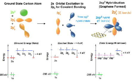
Graphene is composed of covalently bonded, sp2 hybridized, carbon atoms in a two dimensional hexagonal atomic structure that resembles honeycomb. Bonding hybridisation refers to the mixing of valence electron states. Carbon is the 6th element in the periodic table and has six electrons, two electrons with opposite spins fill the first shell (principal quantum number (n = 1) and four partially fill the second shell (n = 2). The shell with n=2 is the valence shell of carbon and two electrons fill the first sub-shell (2s) and the remaining two partially fill the second sub-shell (2p) as reported in Figure 1.2. The electron configuration of a carbon atom is described as 1s22s22p2. The p sub-shell is
1.2 The Physics of Graphene
capable of holding 6 electrons in total, with pairs of electrons with opposite spin states occupying the x (px), y (py) and z (pz) axis (orbital). The 1s sub-shell has an orbital energy of E ≈ -285 eV [4] and thus the 1s2 electrons are not considered in the majority of theoretical predictions and carbon interaction and bonding are attributed to n = 2 shell. The 2p and 2s orbitals have an energy difference (≈ 4 eV [5]) and thus it is energetically favourable to fill the lower energy 2s orbital first. However, in the presence of other carbon atoms it becomes energetically favourable to excite a single 2s electron to fill a third 2p orbital state in order to form covalent bonds known as spx hybridised covalent bonds with the neighbouring atoms (Figure 1.2). The spx orbital has three common forms sp1 (acetylene), sp2 (graphene) and sp3 (diamond) where the order of the sub-shell indicates the number of electrons involved in the hybridised bonding from that sub-shell. Graphene is sp2 hybridised and forms a three fold planar bonding between a single 2s orbital and two 2p orbitals (2px and 2py) with the same electron orbitals of three other neighbouring carbon atoms (Figure 1.2). The hybridisation becomes the core orbital and one electron is left over from the n = 2 valence band per carbon atom, from the energy minimisation from hybridised bonding this becomes a 2pz un-hybridised orbital which has an orbital volume out of plane to the sp2 hybridised covalent sigma bonds and acts to form p covalent bonds with neighbouring 2pz electrons. For clarity 1s22s22p2 (non-hybridised) became 1s22s12p3 (sp2 hybridised) as the external potential from bonding with other carbon atoms favours the hybridised energy state even though it costs ≈ 4 eV to promote a 2s electron to the 2pz orbital state. Figure 1.2 shows the orbital form of ground state carbon orbitals and their respective formation into sp2 hybridised orbitals in the graphene lattice. It is the 2pz orbital that is capable of joining the de-localised extended states that form the valence and conduction bands of graphene and facilitates graphene’s electrical properties.
Figure 1.2. The orbital evolution from a ground state energy carbon atom to a sp2
hybridised graphene atom.
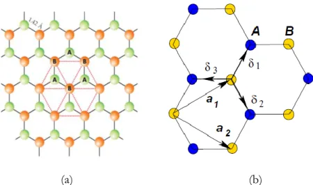
1.2.2 Graphene crystal structure
Graphene is a carbon allotrope in which atoms are arranged forming a honeycomb 2D lattice due to their sp2 hybridization, with an inter-atomic length of acc=1.42 Å. A theoretically pristine crystal is formed from an infinite array of repeating atomic positions. A Bravais lattice can be formed by using the atomic positions. The unique electronic properties of graphene are due to this honeycomb lattice arrangement, which can be seen as two non-equivalent interpenetrating hexagonal lattices with a two-atom basis (A and B), as depicted in Figure 1.3a. Both sublattices are Bravais lattices characterized by two base vectors a and b, with an angle of 120° between them. The lattice vectors forming the basis of the unit cell (Figure 1.3b) are [6]:
𝛼𝑎⃗1=
a
2(3x̂, √3𝑦̂ ) 𝑎⃗2= a
2(3x̂, −√3𝑦̂ ) 1.1
where a ≈ 1.42 Å and is the C-C bond length and the lattice constant can be given as 𝑎⃗ = 𝑎√3 = |𝑎⃗1| = |𝑎⃗2| ≈ 2.46Å, 𝑥̂ and 𝑦̂ are the Cartesian basis
vectors (unit vectors).
Any linear combination of the vectors a1 and a2 generates all the points in the lattice.
1.2 The Physics of Graphene
Figure 1.3. (a) The honeycomb lattice of graphene showing the two sublattices
marked A and B [7]. (b) Lattice structure of graphene showing the two sublattices marked A and B; a1 and a2 the lattice unit vectors; 𝜹𝒊 i=1, 2, 3 the nearest neighbor
vectors [6].
The vectors 𝜹𝟏,𝟐,𝟑 connect in real space any site on the A sublattice to any of its three nearest neighbours which all reside on the B sublattice and they can be defined as: 𝛿1 ⃗⃗⃗⃗ =𝑎 2(+√3𝑦̂) 𝛿⃗⃗⃗⃗⃗ =2 𝑎 2(𝑥̂ − √3𝑦̂) 𝛿⃗⃗⃗⃗⃗ = −𝑎𝑥̂ 3 1.2 Reciprocal space (k-space, momentum space) is a construct used for theoretical analysis of periodic structure. The real space and reciprocal space vectors satisfy the relation 𝑎 ̂𝑖 ∙ 𝑏̂𝑗 = 2𝜋𝛿𝑖𝑗 where 𝛿𝑖𝑗 is the Kronecker delta.
The reciprocal lattice vectors 𝑏⃗⃗1 and 𝑏⃗⃗2 of the graphene Bravais lattice are
defined as 𝑏⃗⃗1= 2π 3a (1𝑥̂, √3𝑦̂) 𝑏⃗⃗2= 2π 3a (1𝑥̂, -√3𝑦̂) 1.3
and shown in Figure 1.4 relative to the first Brillouin zone (BZ). Importantly, the BZ is the reciprocal analogue of the real space Wigner-Seitz cell and can be defined as the area of available reciprocal space that does not cross any Bragg planes drawn about a lattice point.
Figure 1.4. First Brillouin zone of graphene with the reciprocal lattice vectors defined
as b1 and b2. High symmetry k-points are labelled as Γ, M, K and K’ [6].
The area within the first BZ is closer to the origin than any other lattice point and importantly this means that any point in reciprocal space has an equivalent in the first BZ due to the periodic nature of the lattice. Every wave vector within the BZ is unique and non-equivalent to another in the BZ, therefore any wave vector in any periodic state of the crystal has a single wave vector equivalent within the BZ. Here a wave vector 𝑘⃗⃗ (wavenumber k =|𝑘⃗⃗|) is related to momentum via 𝑝⃗ = ℏ𝑘⃗⃗ =2𝜋ℏ𝜆 and is often referred to as the crystal momentum. Considering the reciprocal space of the honeycomb lattice, it is easy to see that the first Brillouin zone is an hexagon [7].
1.2.3 The band structure of graphene
Due to the sp2 hybridization of carbon valence orbitals, the 2s valence orbital mixes with the 2px and 2py ones forming three equivalent sp2 hybrid orbitals lying in the xy plane. Three in-plane carbon atoms are bonded to other nearby carbon atoms by covalent bonds by sigma bond by overlapping their sp2 orbitals and are not available for the conduction process, as well as the electronic bands of the 1s state, which is completely filled. The remaining 2pz orbital, with an axis normal to the xy plane, can overlap with a neighboring 2pz orbital forming 𝜋 bonding and 𝜋∗ antibonding orbitals [14]. Overlap between
2pz orbitals of neighboring carbon atoms in graphene results in the formation of a delocalized 𝜋 system. Each atom in the unit cell is characterized by the 𝜋 bond and thus can donate one electron to the lattice, almost completely
1.2 The Physics of Graphene
delocalized, free to move and actively participate to conduction. Most of the spectacular electronic properties of graphene are related to its 𝜋 and 𝜋∗ electron
energy bands. The form of the 𝜋 energy bands in graphene was first derived by Wallace in 1947 within the approximation of tight-binding electrons [1]. Considering only interactions between 23 nearest neighbors in the lattice this will be 𝐸(𝑘) = ±𝑡√1 + 4 cos (√3 2 𝑎0𝑘𝑥/2) cos ( 1 2𝑎0𝑘𝑦) + 4 cos2( 1 2𝑎0𝑘𝑦) 1.4
where 𝑎0 is the carbon-carbon distance and t ≈ 2.8 eV is the nearest neighbor hopping energy. The minus sign applies to the lower 𝜋 band, which is fully occupied, and the plus sign to the upper 𝜋∗ band, which is empty. These bands
come in contact, without overlapping, at six points in the reciprocal lattice, which are commonly referred to as the K points, coincident with the boundary of the first Brillouin zone. Graphene’s BZ shows four distinct vector positions from the origin, Γ⃗, M⃗⃗⃗⃗, K⃗⃗⃗, K⃗⃗⃗′ and are positioned at:
Γ⃗ = 0𝑥̂ + 0𝑦̂, M⃗⃗⃗⃗ =2𝜋 3𝑎𝑥̂, K ⃗⃗⃗ =2𝜋 3𝑎(𝑥 ̂ + 𝑦̂ √3) , K ⃗⃗⃗′= 2𝜋 3𝑎(𝑥 ̂ − 𝑦̂ √3) 1.5
K and K’ represent a set of non-equivalent points in the reciprocal space which
may not be connected one to another by a reciprocal lattice vector. The corners of the Brillouin zone, where the band crossing occurs are K and K´ points. The
K and K’ points are the primary points of interest when studying the electronic
properties of graphene. This crossing point is called the Dirac point and its energy position is exactly at the Fermi level. A representation of the graphene energy bands is shown in Figure 1.5. Fermi energy lies exactly at the K points for undoped graphene and the Fermi surface of graphene consists thus of only six points.
Figure 1.5. Band structure of graphene. In the vicinity of the Dirac points at the two nonequivalent corners K and K′ of the hexagonal Brillouin zone, the dispersion relation is linear and hence locally equivalent to a Dirac cone [8]. The energy dispersion is a function of the wavevector components kx and ky, as obtained from Eq. 1.3. Valence
(𝝅) and conduction bands (𝝅∗) are seen touching at the Fermi level at the K and K’
points with a linear conical relation among them.
Near these points the relationship of the energy versus momentum becomes linear, which has significant consequences for the electronic transport and optical properties of graphene. The linear dispersion region is well-described by the Dirac equation for massless Dirac fermions, particles with relativistic speed and no mass [9]
E(k)=±ℏ𝑣𝐹|𝑘⃗⃗ − 𝐾⃗⃗⃗| 1.6
with ℏ reduced Planck constant, k the wave vector of the electron and 𝑣𝐹 ≈
106𝑚𝑠−1 is the Fermi velocity (responsible of the ballistic transport) [10]. In the usual case with parabolic valence and conduction bands the dispersion
relation is 𝐸(𝑘⃗⃗) = 𝐸(0) +ℏ2𝑘⃗⃗2
2𝑚∗ and the velocity 𝑣 = √2𝐸/𝑚 is proportional to the energy. Comparing these relations to Einstein’s relativistic energy relation (𝐸 = √(𝑚𝑐2)2+ (𝑐𝑝)2) for massive particles in the nonrelativistic
limit 𝐸 ≈ 𝑚𝑐2+ 𝑝2
2𝑚 and massless relativistic particles 𝐸 = 𝑐|𝑝| there is a clear
1.2 The Physics of Graphene
graphene’s dispersion relation and massless particles [6]. Therefore in the low energy limit in the Dirac valleys the electronic states can be described by the Dirac equation for m = 0, as a consequence the charge carriers in graphene are quasiparticles and are known as massless Dirac fermions. It should be noted that frequently graphene is described as having a zero effective mass using
𝑚∗ = ℏ2(𝑑2𝐸−1
𝑑𝑘2 ) as is used in semi-conductors, however this gives 𝑚
∗= 1 in
the linear Dirac valleys or zero at the Dirac point. The effective mass of graphene’s charge carriers becomes anomalous at the Dirac points (𝐸 = 𝐸𝐹) as
the wavenumber k = 0 and instead can be described as [6]:
𝑚∗ = 1
2𝜋
𝜕𝐴(𝐸)
𝜕𝐸 1.7
where 𝐴(𝐸) = 𝜋𝐸2/𝑣
𝐹2 and is the area in reciprocal space enclosed by the 2pz
orbit. The charge carrier effective mass can then be related to 𝐸𝐹, the carrier
density n and the Fermi momentum 𝑘𝐹(𝑘𝐹2 = 𝑛𝜋) by [6]:
𝑚∗ = 𝐸𝐹 𝑣𝐹2 = 𝑘𝐹 𝑣𝐹 = √ 𝜋𝑛 𝑣𝐹2 1.8
Again, note ℏ needs to be applied for the correct units. It can be seen clearly that at the Dirac Point where n=0 the effective mass is zero.
Linear dispersion graphene 𝜋 bands close to the Dirac points result, also, in a linear dependence of density of states on the energy. The density of states per unit cell can be written as [6]
𝜌(𝐸) =2𝐴𝐶|𝐸| 𝜋ℏ2𝑣
𝐹2
1.9
where 𝐴𝐶 is the unit cell area. At the Dirac point the density of states is in principle zero. Despite that, graphene exhibits a minimum quantum conductivity of the order of 4e2/h [11]. The linear dispersion of the Dirac valleys creates a linear change in the density of states until reaching the Dirac
point where the density of states is zero. Increasing E above 𝐸𝐹 induces electrons into conduction band, decreasing E below 𝐸𝐹 increases the hole
density. At the Dirac point (at 0 K thus zero probability of excitation states above 𝐸𝐹) graphene should exhibit an infinite resistance/zero conductivity as
the zero density of states indicates a zero charge carrier density [12].
1.3 Graphene Properties
Since graphene discover, its electronic properties have attracted the interest of researchers, who looked at graphene as the substitute of silicon in the fabrication of electronic devices.
1.3.1 Electronic transport properties of graphene
The electronic transport and optical properties of graphene are greatly influenced by the physics of the charge carriers near the Dirac points. Charge carrier mobility (𝜇) of up to 1000000 cm2/Vs at low temperature (~5 K) [13] has been observed in pristine, suspended graphene, where interactions with the substrate are eliminated. At room temperature, the mobility has been measured to typically range from 10000 to 200000 cm2/Vs [14], [15] [16]. This value is at least 100 times faster than what is observed in silicon. Scattering in graphene does not depend strongly on temperature for T < 400 K [17] but it is influenced by the charged impurities of the supporting substrate and other extrinsic impurities that may be present [6], [14], [15], [17], [18]. For instance, the carrier mobility is typically on the order of 10000 cm2/Vs for polar SiO
2 substrate limited by the graphene-SiO2 interaction [6] On the other hand, graphene placed on more inert, hexagonal boron nitride (BN) substrate exhibited the mobility of 500000 cm2/Vs [19], [20]. Substitutional defects are unlikely in graphene as the carbon atoms form strong in-plane bonds and graphene seems to form perfect crystal without vacancies in the range of microns at room temperature [21]. Furthermore, graphene forms corrugations or puddles of charges which can act also as scattering centres [22]. Conductivity of graphene can be tuned by doping through fabrication of a field effect device structure
1.3 Graphene Properties
where the application of gate voltage modulates the Fermi level (Figure 1.6). Figure 1.6a depicts the density of states and ambipolar transport in graphene where it can be seen that both the hole and electron densities can be easily controlled with the gate voltage [23]. Because the density of state increases linearly away from the charge neutrality point, the conductivity also varies linearly with gate voltage (Figure 1.6b). The mobility, however, remains constant over a wide range of gate induced doping. At low temperatures, graphene approaches a universal conductivity of 4e2/h and does not undergo metal to insulator transition as theoretically expected for a material even with very low concentration of charge carriers near the Dirac point [11]. This minimum quantized conductivity has been predicted by the theory describing the 2D Dirac fermions. The high mobility makes graphene a potential material for nanoelectronics especially in high-frequency applications [24].
Figure 1.6. (a)Calculated density of states of graphene. Close to the Fermi level, the density of states ρ(ε), is linear with respect to the energy [6]. (b) Ambipolar transport characteristic of graphene. Field induced by gate voltage, Vg can control concentration and polarity of charge carriers. Positive (negative) gate voltage increases Fermi level increasing carrier concentration of holes (electrons) [11]
1.3.2 Scattering in graphene
The charge-carrier mobility in graphene, which is around 10000 cm2/Vs at room temperature, is believed to be limited by scattering of charge carriers [25]–[27]. There are various sources of scattering in a graphene system, such as phonons, charged impurities, neutral point defects and ripples (microscopic corrugations of a graphene sheet). Although intrinsic scattering such as scattering produced by interaction with phonons cannot be eliminated at room temperature, which eventually raises a fundamental limit on the mobility in
graphene, the electron-phonon scattering in graphene is found to be weak enough that mobility can still reach around 200000 cm 2/Vs at room temperature if extrinsic disorder is eliminated [14]. On the other hand, extrinsic disorders such as charged impurities, ripples and neutral point defects are considered the source of scattering that is expected to suppress the mobility in graphene. Short-range scattering generated by neutral point defects, or impurities, has limited effect on graphene's resistivity 𝜌, comparing to conventional nonrelativistic two-dimensional electron system [27], [28]. This fact may help to understand the remarkably high mobility in graphene. On the other hand, long-range Coulomb scattering from the random charged impurities located near the interface between the graphene and the substrate can be another possible candidate that limits the charge carrier mobility in graphene [26], [29], [30]. It explains the experimental fact that resistivity 𝜌 is inversely proportional to charge carrier density n and mobility is independent of charge carrier density. The typical concentration of charged impurities in graphene samples with mobility limited to ~ 10000 cm 2/Vs is estimated to be ~ 1012 cm-2 [30]. In addition to charged impurities, ripples in graphene should create a similar long-range scattering effect on the mobility [31]. Large-scale ripples were also observed in graphene on SiO2 [32], while nanometre-sized ripples were observed in scanning-probe study of graphene [33], [34]. This kind of ripples is unavoidable, because strictly 2D crystals are extremely flexible and soft, and the existence of ripples can help stabilize the crystal by lowering the total energy.
1.3.3. Optoelectronic properties of graphene
Graphene shows remarkable optical properties. For instance, despite being only a single atom thick, it can be optically visualized. For freestanding single layer graphene (SLG) transmittance (T) can be derived by applying the Fresnel equations in the thin-film limit for a material with a fixed universal optical conductance [10]:
1.3 Graphene Properties
T = (1 + 0.5 πα)-2 ≈ 1 – πα ≈ 97.7% 1.10
where 𝛼 is the fine-structure constant [35]. Graphene only reflects <0.1% of the incident light in the visible region, rising to ~2% for ten layers. Thus, it can be assumed the optical absorption of graphene layers to be proportional to the number of layers, each absorbing A≈1 – T ≈ 𝜋𝛼 ≈ 2.3% over the visible spectrum (Figure 1.7).
Figure 1.7. Scan profile showing the intensity of transmitted white light through air,
single layer and bilayer graphene respectively [35].
Its transparency makes graphene ideal for its use in optoelectronic devices such as displays, touchscreen and solar cells, where materials with low sheet resistance Rs and high transparency are needed. It could replace the current transparent conducting materials, as indium tin oxide (ITO) [10], [36]. ITO is commercially available with T≈80% and Rs as low as 10 Ω/sq on glass and ~60−300 Ω/sq on polyethylene terephthalate. However, ITO suffers severe limitations: an ever-increasing cost due to indium scarcity, processing requirements, difficulties in patterning and a sensitivity to both acidic and basic environments. Moreover, it is brittle and can easily crack when used in applications involving bending, such as touch screens and flexible displays [10]. For these reasons new transparent conducting materials with improved performance are needed and graphene seems to be a good alternative. Graphene films have a higher transmittance over a wider wavelength range than
single-walled carbon nanotube (SWNT) films, thin metallic films (ZnO/Ag/ZnO e TiO2/Ag/TiO2) and ITO (Figure 1.8a) [10].
Figure 1.8. (a) Transmittance for different transparent conductors and (b) thickness dependence of the sheet resistance [10].
It has been calculated that for an ideal intrinsic SLG with T ≈97.7% resistance sheet value is about 6 kΩ/sq. Thus, an ideal intrinsic SLG would beat the best ITO only in terms of T, not Rs. However, real thin films are never intrinsic. The range of T and Rs that can be realistically achieved for graphene layers of varying thickness can be estimated by taking n= 1012-1013 cm−2 and μ = 1000 - 20000 cm2 V–1 s–1. As shown in Figure 1.8b, graphene can achieve the same Rs as ITO, ZnO/Ag/ZnO, TiO2/Ag/TiO2 and SWNTs with a similar or even higher transmittance [10]. It has been also demonstrated that the optical properties of graphene can be significantly modulated by the doping which can lead to novel optoelectronic effects and devices [37].
1.3.4 Thermal conductivity in graphene
Thermal conductivity of graphene can also occur through ballistic phonon transport with theoretical values of the thermal conductivity predicted to be ~8000 W/mK while indirect measurements have yielded values ranging from 600 to 5000 W/mK that are comparable to that of bulk graphite (≤2000 W/mK) [38]–[42]. This thermal properties makes graphene promising for thermal management and in particular for heat dissipation and transport applications [43], [44].
1.3 Graphene Properties
1.3.5 Physical properties of graphene
Graphene attracts much interest also for its mechanical properties. Numerical methods and experimental techniques have proved graphene intrinsic mechanical properties, characterized by high strength, hardness and elasticity [45], [46]. For instance, the spring constant of suspended graphene sheets is in the range 1-5 N/m and the value of the Young’s modulus equal to 1.0 teraPascal (TPa) was measured for monolayer graphene by Atomic Force Microscopy (AFM), assessing graphene as the strongest material ever measured [45]. These mechanical properties make graphene a strong material and lead to a promising potential of utilising graphene in Nanoelectromechanical systems (NEMS) [47].
1.3.6 Chemical and Surface Properties
Like graphite, graphene is generally a chemically stable material and it is thermally stable in air up to temperatures of ~500 ˚C [48]. Graphene has a very large surface area, ~2600 m2/g [49] which is useful for catalyst and energy storage applications. Graphene can also serve as a support for sensing adsorbing gas molecules [50] or for forming nanoparticle assemblies [51]. Graphene can be functionalized through chemical modifications such as oxidation, hydrogenation, and fluorination. Oxidation renders graphene hydrophilic and allows further alteration of the functional groups by organic molecules (e.g. acylation followed by SOCl2 activation for polymer linkage and treatment by diazonium salts for improved solubility in polar organic solvents) [52], [53]. Hydrogenation can render graphene insulating [54], [55] and may have implications in hydrogen storage [56]. Fluorination of graphene makes it strongly hydrophobic, induces p-type doping, and can also open up a band gap [57], [58]. Through functionalization, the optoelectronic, chemical, and surface properties of graphene can be engineered for multitude of applications.
In conclusion, crystal and electronic structure of the graphene, give it interesting properties, such as:
Density of 0.77 mg/m2 Thickness of ≈ 3.4 Å
Surface area to volume ratio 2630 m2/g
Massless, relativistic Dirac quasiparticle charge carriers [2] Room temperature mobility ≈ 200000 cm2/Vs [14], [17] Low temperature mobility ≈ 6·106 cm2/Vs (T = 4 K) [59]
Higher current density capacity (milliamps through ribbons microns wide) [60]
Tunable band gap with length [61]
Tunable hole and electron densities with an applied electric field [2], [23]
Half integer quantum Hall effect at room temperature [9]
Room temperature quantum Hall effect [62] and unconventional Hall effects [63], [64]
Transparent - absorbs ≈ 2.3% of normal incident light [10], [16], [65] Softest material possible against transverse deflection, flexible and
stretchable [66]
Young’s modulus ≈ 1TPa [45] Intrinsic strength of 130 GPa [45]
Thermal conductivity ≈ 5000 W/mK [43] Cheap to produce [67]
1.4 Graphene Synthesis
Graphene does not exist in nature as isolated 2D material, but it can be extracted from graphite. Mechanical cleavage, thermal decomposition of silicon carbide, liquid phase exfoliation of graphite, molecular assembly and chemical vapor deposition (CVD) are the most commonly used synthesis methods of graphene. Anyway, it should be pointed out that no one of the aforementioned synthesis techniques can be considered as the best one in absolute. Since each of these methods is suitable to obtain graphene with different characteristics, the choice of a specific technique derives by the role of graphene in the specific application.
1.4 Graphene Synthesis
Figure 1.9 compares the available methods with regards to graphene quality and cost. CVD is described in detail due to its relevance to the study and further detail of the process is included in the results section.
Figure 1.9. Graphene quality vs mass production cost of different graphene
fabrication methods [68].
1.4.1 Mechanical exfoliation
Mechanical exfoliation can be regarded as the mother of all techniques for graphene production, since it was the first technique through which graphene was successfully isolated by Geim and Novoselov [2]. It basically consists in the exfoliation of a High Oriented Pyrolytic Graphite (HOPG) block through the so called “scotch-tape technique”. HOPG can be considered as a significant stack of monolayer graphene with distance of 3.34 Å, and stacked interacting with each other via van der Waals forces. Such forces are weak and for graphite the energy needed to cleave layers from each other is 0.39 ± 0.02 J/m2 [69] (ABAB stacked). Thus graphene layers are easily peeled/cleaved/exfoliated from each other without any effort and this is the fundamental principle of this method [2]. In this method, an adhesive can be used to peel off the graphite flakes, as depicted in Figure 1.10a. With the first
step, several layers of bulk graphite are removed from the planar side of HOPG sample. The first piece of tape is then repeatedly cleaved by other sticky pieces till to obtain an almost invisible powder on the starting tape. With any luck a few flakes of single or bi-layer graphene will be isolated Finally, at the end of the exfoliation process, the tape is transferred onto another substrate that usually is silicon dioxide on Si wafer (SiO2/Si). In Figure 1.10b an optical image of a mechanical exfoliated multilayer graphene flake is show
Figure 1.10. (a) Scotch tape mechanical exfoliation [70], (b) Exfoliated graphene
on 300 nm thick SiO2, the number of layers increases with flake contrast, the number of layers are labelled, image adapted from [71].
The costless and advantageous of the technique brought many research groups to use it to produce high quality graphene layers. Graphene produced by this technique show mechanical and electrical quality comparable to the theoretical predictions. However, the real dimensions are significantly limited. The largest measured monolayer flakes are no bigger than 1 mm in any planar dimension [72] and the position of the flakes are uncontrollable. In order to be used for the fabrication of nanoelectronic devices, this process needs improvements for both the large-scale production and transfer method.
1.4.2 Liquid Phase Exfoliation
One of the promising routes to synthesize large quantities of graphene for large area applications is to exfoliate graphite in solution to produce a dispersion of graphene flakes. Graphite can be exfoliated in liquid environments exploiting ultrasounds to extract individual layers, (Figure 1.11). Such exfoliation method relies on covalent and non-covalent interactions
1.4 Graphene Synthesis
introduced by external molecules to disrupt the van der Waals interactions between the graphene sheets. The liquid-phase exfoliation (LPE) process generally involves the dispersion of graphite in special solvents able to minimize the interfacial tension between the liquid and graphene flakes. Indeed, if the interfacial tension is high, the flakes tend to adhere to each other and the work of cohesion between them is high, hindering their dispersion in liquid. Liquids with surface tension γ ~ 40 mN/m, are the best solvents for the dispersion of graphene and graphitic flakes, since they minimize the interfacial tension between solvent and graphene [70]. The solvents that mainly match this requirement are N-methyl-pyrrolidone (NMP) and Dimethylformamide (DMF) even if toxic and harmful to the environment. In order to favor the splitting of graphite into individual platelets, the solution should be sonicated for a long time. Finally, the surnatant phase of the suspension, the thinner exfoliated flakes, must be separated from the unexfoliated ones. Centrifugation process is generally used to this purpose [73]. Since this technique is regarded as one of the most promising for mass production, high concentration of exfoliated graphene is desirable. It is important to note that the yield of the process is strongly affected by each parameter involved in the procedure.
Figure 1.11. Liquid phase exfoliation technique [70].
1.4.3 Epitaxial Growth on SiC
Graphene can be synthesized by the thermal decomposition of silicon carbide [70], [74] (Figure 1.12). This growth technique is usually referred to as “epitaxial growth” even though there is a very large lattice mismatch between
SiC (3.073 Å) and graphene (2.46 Å) and the carbon rearranges itself in a hexagonal structure as Si evaporates from the SiC substrate, rather than being deposited on the SiC surface, as would happen in a traditional epitaxial growth process. The process is possible due to the lower sublimation temperature of Si compared to C and when elevated temperatures ≈ 1200°C and ultra-high vacuum (UHV) are applied to SiC. The annealing of the substrates results in the sublimation of the silicon atoms while the carbon-enriched surface undergoes reorganization and, for high enough temperatures, graphitization [70]. The typical range of annealing temperatures goes from 1500°C to 2000°C and the usual heating and cooling rates are 2-3°C/sec [75]. The thermal decomposition, however, is not a self-limiting process and areas of different film thicknesses may exist on the same SiC crystal. The graphene growth is also very sensitive to the crystallographic orientation of SiC and processing before growth is often essential [76].
Figure 1.12. Growth on SiC. Gold and grey spheres represent Si and C atoms,
respectively [70].
The dimensions of graphene produced are moderately larger in comparison to mechanically exfoliated graphene and can be on the order of 100 µm [11] but are not significant enough for non-research use. Graphene obtained on SiC single crystals has has shown a mobility of > 3400 cm2/Vs [77]. Mobility has seen more recent improvements to 11000cm2/Vs but this is at a temperature of 0.3K and after a H2 intercalation process [78]. Graphene produced by epitaxial growth on SiC may be limited to devices on SiC only, since transfer to other substrates such as SiO2/Si might be difficult, with all the
1.4 Graphene Synthesis
drawbacks involved in the transfer process. Moreover, it is an expensive technique because of the SiC wafers cost.
1.4.4 Chemical Vapour Deposition (CVD)
Chemical Vapor Deposition (CVD) is a widely used method to grow thin films from many different carbon precursors both in vapor and liquid phase, such as methane (CH4), methanol (CH3OH) and ethanol (C2H5OH) [54], [79]– [85] that are dissociated at high temperature using transition metal substrates such as Fe [86], Co [87], Ni [88]–[93], Cu [54], [94]–[100], Ru [87], Ir [87], [101], Pt [102]–[104] and Au [105], [106].
Graphene growth morphology is heavily dependent upon the growth substrate, with the grain orientation, grain size, grain boundary density and importantly the number of layers all being variable. At elevated temperatures and pressures, C dissolves into the surface of the substrate during CVD. The amount of C that the substrate intakes is defined as its solubility. The C solubility is a critical factor for optimizing graphene growth in terms of crystalline quality and number of layers. Low C solubility suppresses the formation of multi-layer graphene as C adatoms are predominantly restricted to the substrate surface. Graphene forms into small nuclei, which coalesce and grow into a full surface coverage at which point the precursor gas can no longer dissociate at the catalyst surface and thus no more C atoms can be added to the system, creating a self-terminating monolayer graphene growth. On very low C solubility materials, minimal bi-layer formation is shown such as on Cu it is often found that the graphene coverage is ≈ 95% monolayer Cu [54], [65], [94]– [100], [107], but this can be quite variable with CVD parameters such as temperature, pressure, growth time and C concentration. Graphene growth is also strongly affected by interaction with metallic substrate and surface orientation [87]. It is important to take into account lattice mismatch between graphene and substrate caused by C atoms forced from the most energetically favorable adsorption positions on the metal surface when incorporated into a graphene lattice. Weaker bonding creates an elongated distance between the metal surface and graphene and this often corresponds to a decreased C