SN Applied Sciences (2019) 1:844 | https://doi.org/10.1007/s42452-019-0882-9
Radiation‑direction steerable nanoantennae
Luigi Bibbò1 · Qiang Liu1 · Karim Khan1 · Ashish Yadav1 · Sayed Elshahat1 · Israa Abood1 · Zhengbiao Ouyang1 © Springer Nature Switzerland AG 2019
Abstract
In this work, we design a novel reflection nanoantenna with a metasurface containing an array of silver nanoparticles. Moreover, an electro-optical (EO) layer is introduced to produce radiation-direction steerability. Finite-element simu-lations are conducted to verify the optical responses through radiation pattern, directivity, and gain of the proposed structure, showing a good tunable directional nanoantenna with a single control voltage applied on a thin EO layer, without requiring complicated rotating structures or hundreds of phase-shifting units. The joint action of the plasmon surface waves and the EO layer in the nanoantennae leads to the voltage-angle steerability for its radiation directions. The nanoantennae can find applications in biologic sensors, microscopy, spectroscopy, energy transfer, wireless connection in and among chips, light extraction from single photon source and subwavelength sized lasers, micro radar systems for micro- robots or submarines used inside human body for navigation in the veins or arteries, and compensation of fabrication errors.
Keywords Plasmonics · Coupled resonators · Metamaterials · Electro-optical devices · Nanoantennae
1 Background
In recent years metamaterials have attracted consider-able interest in the realization of optical devices due to their capability to overcome the diffraction limit of light [1]. These materials have special properties which are not found in natural materials. They are artificially constructed and are attractive for manufacturing of optical subwave-length devices with practical functionality, offering the possibility for improving performance in multifunctional nanophotonic applications. Their well-controllable per-mittivity and permeability [2] make them suitable for the manufacture of optical antennae [3].
Metasurface, which is one layer or a few layers of the metamaterial, has recently been proposed to manipulate arbitrary light wavefront at will [4], leading to various fas-cinating applications such as metalens [5–7], metasurface beam shapers [5, 6], and meta-holograms [8, 9].
It has been seen that the resonance in metamaterials is affected by the permittivity of the surrounding medium. If a tunable dielectric material is incorporated in the unit cell of metamaterials, one can achieve tunable metamaterials and the resonance wavelength can be tuned [10].
A tool was made by Gurbakov and co-authors to map the refractive-index variations of a smooth dielectric sur-face by detecting the spectral response of a single Ag sphere optically aligned with a supporting optical fiber axicon microlens [11].
Tunable metamaterials capable of manipulating the propagating waves can be used to control the radiation pattern, directivity, and polarizations [12, 13].
With these characteristics they can be used for fabri-cation of tunable directive nano-antennae. Krasnok and coauthors have proposed a highly tunable dielectric nano-antennae consisting of a chain of Si nanoparticles, excited by a dipole emitter, which allows for tuning its radiation
Received: 13 February 2019 / Accepted: 4 July 2019
* Zhengbiao Ouyang, [email protected] | 1College of Physics and Optoelectronic Engineering of Shenzhen University, THz Technical
Research Center of Shenzhen University, Key Laboratory of Optoelectronics Devices and Systems of Ministry of Education and Guangdong Province, Shenzhen University, Shenzhen 51806, China.
properties via electron–hole plasmonic photoexcitation [14].
Nanoantennae can be seen as a miniaturized version of conventional antennae for enhancing directivity in transmitting or receiving signals. With the technological evolution of the production of nanoscale elements, it has been possible to extend the physical characteristics of RF antennae to optics by creating optical nanoantennae [15].
Optical antennae operating in the visible and near infrared bands are known as plasmonic antennae based on localized surface plasmon (LSP) for strong-near field interaction [16, 17].
They act as resonant structures which allow transmis-sion and reflection of electromagnetic waves in a specific way in a certain frequency band [18, 19]. For optical strain sensor applications, the tailored plasmonic nanostruc-ture with continuously tunable resonances is created by preparing bow-tie shaped nanostructures on a flexible substrate of polydimethylsiloxane (PDMS). Due to strain change, the deformation of substrates leads to an increase or decrease of the nanostructure gap, and therefore to a decrease or increase of the antennae coupling [20].
The strongly coupled plasma and the capability of manipulating light on the nanoscale make nanoantennae particularly useful in fields such as biologic sensors [21], narrowband absorbers [22], microscopy and spectroscopy [23], heat transfer [24] and photovoltaics [25, 26]. Moreo-ver, nanoantennae are key components for wireless con-nection at the nanoscale. They can operate in the on-chip optical network for micro and nano circuits [27, 28]. For example, the nano directivity-tunable radiation can be applied to generate multi-beam signals to establish a con-nection between one chip and a number of other chips, or time sequential pulses for controlling a number of logic elements. On the contrary, a tunable nano-antenna can be used as a specific channel signal extractor that picks up a signal of a specific channel from a number of chan-nels for digital signal processing, optical communication, and optical computation. Furthermore, they can be used to extract light from the single photon source [29, 30] and subwavelength sized lasers.
Furthermore, micro radar systems for micro-robots or submarines used inside human body systems can be developed using the nano directivity-tunable radiation structure as antennae where the wave beam direction can scan by varying the control voltage for navigation in the veins or arteries [31, 32]. They can enter the body to diagnose diseases and tissues or organs like blocked arteries, and deliver drugs for the treatment of specific disorders. The tiny robot crawls through arteries and veins; its minuscule outstretched arms grip the sides of vessel walls as it zeroes in on its targeted location. Here micro antennae and radar are required. In addition,
tunability is necessary for compensating fabrication errors: as there exist always fabrication errors and the beam may deviate from a specific direction, therefore, the beam direction adjustment or tunability is required to compensate the direction deviation.
Recently there is a growing interest in fabricating nanostructures that are pre-programmed to alter the properties of light in a specific way when the light inter-acts with them.
There are many ways to control and tune the radia-tion patterns of antennae: by changing the angle of inci-dence and polarization of the excitation beam, or using evanescent waves to illuminate the system, which is advantageous for the separation of excitation from the antennae signal [33]. Others to realize reconfigurable metasurface have utilized graphene and doped semicon-ductors (GaAs and InSb) under the influence of external voltage bias and still others use the integration of ITO as an active material with controllable carrier concen-trations into a metasurface under an externally applied voltage [34]. For overcoming manufacturing difficulties, other solutions have been suggested based on the inte-gration of varactors into metasurfaces; in fact, Daniel F. Sievenpiper and co-authors have designed an electri-cally beam steering antennae.
The impedance of the metasurface is modeled as LC resonant circuit, integrating varactor circuit in the sur-face which created a tunable impedance sursur-face where an applied bias voltage controls the resonance frequency and reflection phase [35]. Also, active frequency selec-tive surfaces (AFSS) have been used to modify EM wave propagation.
Although some authors have discussed the control of directivity using metasurface, no one has focused on controlling the directivity by a single voltage and a single electro-optical (EO) layer using the Pockels effect. Conven-tionally, each element of a phase-control array antenna with a voltage and a control circuit is quite complicated. As an example, Hashemi et al. suggested a solution capa-ble of deflecting electromagnetic waves by controlling the applied current to each individual metasurface unit-cell [36]. Burokur et al. instead designed models based on the operating principle of Fabry–Perot reflex-cavity antennae. The cavity antenna is formed by a feeding source placed between two reflecting surfaces. The cavity is composed of a perfect electric conductor (PEC) as a conventional ground plane for the feeding source and a metasurface, partially reflective surface (PRS) playing the role of trans-mitting window. The directivity of the beam is obtained through the phase variation of the wave traveling inside the cavity. The variable phase is obtained by applying dif-ferent bias voltage along a PRS where lumped elements from varactor diodes are incorporated, i.e., a large number
of different voltages are required in the control of directiv-ity [37].
Using a single bias voltage to change plasmon reso-nances, in this paper we propose a nanoantenna array composed of periodically arranged metallic nanoparticles of Ag in triple-layer configurations of metal-dielectric-metal (MDM), in the IR range. To avoid using a large num-ber of different voltage in control, we utilize the plasmon surface wave and an EO layer.
The plasmon surface wave, excited by incident light, is propagating along the metasurface. In the propaga-tion process, the plasmon surface wave will excite the antennae. Due to the propagation of the plasmon surface wave, the radiated wave by each antenna in the antenna array will have a different phase, obtaining an effect of a large number of bias voltages to the antenna array. The innovative aspect of this work is combining the plasmon resonance of Ag nanoparticles with EO properties of the substance inserted above the bottom layer of Ag, show-ing features of a directional antennae without requirshow-ing complicated rotating structures or hundreds of phase-shifting units. The work has revealed that for the structure designed, the steerability of the antenna can be tuned by the applied voltage. This solution is useful where different communication systems coexist because multiple anten-nae required can be replaced by a single reconfigurable antenna. The device also presents simplicity in design and has the characteristics of compactness and dimensions compatible with modern nanofabrication techniques.
2 Design and formulation
2.1 Physical model
The properties of a nanoantenna are defined by its geom-etry and materials, and numerical simulations are needed to devise and analyze the geometry of the hypothesized structure.
In the numerical modelling, to make the simulation process effective, as already highlighted in other works, the following aspects have been considered: a proper fitting between the simulated material parameters and those obtained in the literature must be set for the fre-quency range of interest; a very fine mesh, usually of a few nanometers, must be set; the stability factor, which defines together with the mesh, the time step, and the simulation time must be properly chosen [38].
It must be highlighted that after the fabrication pro-cess and because of tolerances, the initial design may dif-fer from the real sample. Therefore, structural parameters of fabricated structures should be measured in order to
adjust the simulation parameters and obtain more accu-rate numerical results.
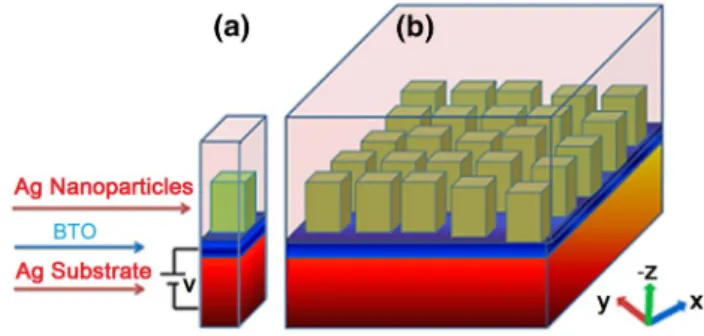
The schematic geometry is shown in the right side of Fig. 1. The unit cell of the structure showed in the left side of Fig. 1 consists of three layers formed by a top layer of nanoantennae of silver nanopillar placed over a metal ground plane substrate separated by a thin dielectric layer [39]. To have better performance, the thickness of the sil-ver nanopillar is to be optimized.
Moreover, in our structure, the main goal is to control the direction of antennae so that quantum dots aren’t added in the antennae to simplify the analysis.
The structure has dimensional parameters as follows: the length, width and height of the rectangular unit antenna are respectively 170 nm, 150 nm and 300 nm, the thickness of the dielectric spacer is 80 nm, and the thick-ness of metallic substrate is 420 nm. The periodicity of the nanoantenna array is 650 nm in both in-plane directions.
We choose, as already described in our previous work [40] even if with geometry of different models, silver as the material for metallic nanoparticle array and the ground substrate, with the permittivity and permeability derived from Drude–Lorentz model, while the dielectric layer is an electro-optic medium BTO [41]. The BTO has EO effect (Pockels effect) and other optical properties, including high nonlinearity, negative birefringence, two refractive indices, two ordinary optical axes which are set along the x axis and y axis in this paper, and an extraordinary opti-cal axis along the z axis. The presence of the Pockels effect allows the tunability of the device, through the variation of the refractive index of dielectric by applying an external electric voltage. The surrounding material is assumed to be air. Each nanopillar is rectangular in shape for the easiness of fabrication.
2.2 Numerical model
The model can be viewed as a two-dimensional structure with the unit cell in Fig. 1a. For simulations, we adopt the standard model as we used previously [42]. The optical
property, parameters and features of the nanoantenna were calculated using the RF module in the commercial finite-element method solver COMSOL Multiphysics. Some basic points for the model and simulation are as follows: “the Perfect Matched Layer (PML) boundary con-ditions were used on the top and bottom surfaces. A sym-metric periodic boundary condition was used along the x- and y- directions. It is noted that periodicity is a basic requirement for metasurfaces, and thus periodic bound-ary conditions are applied in the simulations. The reflec-tion spectra were computed via the “S Parameter” analysis object, which makes use of a plane-wave excitation source incident from upside to the silver pillars. The mesh con-sists of 47,261 tetrahedral elements, and 438,753 degrees of freedom were consumed in the simulation while the server keeps working for 10 h and 50 min. Additionally, an important aspect of the numerical model is that the average element quality of the proposed mesh is 0.8062, which guarantees the stability of the results.”
The radiation patterns of reflection waves are computed by use of far-field scattered formulation in the xoy plane.
For practical implementation, an ITO film could be used above the EO layer, so that the control voltage on the EO layer could be applied. However, for simplicity in analysis, in this paper we omitted the ITO film.
3 Demonstration of steerability
and discussion
3.1 Fundamental and parameter definition
The nanoantenna layer and the Ag substrate sandwiched by the EO layer form a Fabry–Perot resonator.
The hypothesized structure, using resonant subwave-length elements, is steerable and able to convert source waves into desired radiation patterns for applications that require beam forming for communication networks or power transfer. Moreover it is innovative for the simplicity of fabrication and steerability.
The structure is based on the possibility of varying the resonance frequency by changing the permittivity of the dielectric in the structure. Since the variation of the per-mittivity can occur by means of external-voltage control, this allows that the metasurface antenna can be recon-figured dynamically without the need of complex active circuitry.
The Ohmic losses are often neglected in radio fre-quency applications, but in optical applications for the lower conductivity of metals, we observed a great dissi-pated power which can exceed the radiated power.
In terms of the circuit theory, the dissipative losses and radiation losses represented by Ohmic resistance and
radiation resistance represent the real part of the complex input impedance of the antenna. At resonance, the imagi-nary part of the impedance is equal to zero, so as to have a radiant power. It is necessary that the radiation resistance is predominant on dissipative.
To describe, from a theoretical point of view, the phe-nomenon of energy associated with the propagation of the electromagnetic field, we can use the Poynting vector which represents precisely the energy flow for the unity of surface and for the unity of time, carried by a wave.
A polarized incident light perpendicular to the top of device was selected to excite resonant plasmonic waves.
Physically, the mechanism for steerability tuning can be explained as follows. The incident light first excites mon surface waves on the metasurface, then the plas-mon surface waves excite waves in the Fabry–Perot cavity between the nanoparticles (or the silver nanopillars) and the metal substrate, and finally, these waves are reflected back upwards and cause the radiations to the space above the metasurface. Note that the plasmon surface waves are propagating along the metasurface and their phases are affected by the EO layer. As a result, the phase of wave in each sub-antenna, the unit cell of the structure, on the metasurface is different, obtaining an effect of a large number of bias voltage applied to the antenna array. Moreover, it is the wave vector component parallel to the metasurface that set the reflected wave to be in a direc-tion different from the incident angle. Therefore, changing the refractive index by an applied voltage can change the wave vector component parallel to the metasurface and thus the direction of the reflected-wave, and by a single voltage on a thin EO layer, one can obtain an effect of dif-ferent phase change for difdif-ferent sub-antennae, i.e., the effect of the voltage control array in phase-control array antennae, to tune the radiation direction of the antenna proposed.
In another view, the structure proposed can be regarded as a tunable two-dimensional (2-D) reflection grating. Theoretically, the 2-D grating can be considered as a 1-D grating in the x-direction and simultaneously 1-D grating in the y-direction. For 1-D grating in the x-direc-tion, we have the grating equation to decide the maxi-mum radiation angle:
where ne is the effective refractive index of material near the reflection surface and is related to the refractive index of the EO material (BTO) between the nanoparticles and the Ag substrate, d1 is the grating constant in the x-direc-tion, equal to the lattice constant in the x-direcx-direc-tion, α1 and
β1 are the incident and reflection angles in the xoz plane with respect to the normal of the surface xoy (for normal incidence, α1 = 0), m1 is an integer, and λ is the wavelength (1) ned1 ( sin 𝛼1+ sin 𝛽1 ) = m1𝜆,
of the incident light. For 1-D grating in the y-direction, we have the grating equation to decide the maximum radia-tion angle:
where d2 is the grating constant along the y-direction, equal to the lattice constant in the y-direction, α2 and β2 are the incident and reflection angles in the yoz plane with respect to the normal of the surface xoy (for normal inci-dence, α2 = 0), and m2 is an integer. In our model, we use square lattice, so we have: d1 = d2 = d.
Considering that the upper surface of the substrate Ag can be regarded as the reflection surface, we can have ne = n, the refractive index of the BTO. When the refractive index of BTO changes with the tuning voltage, the equivalent refractive index ne will change. Therefore, from Eqs. (1) and (2), it can be seen that the maximum radiation angles shall change, explaining the radiation-direction steerability of the antenna.
This is very useful for controlling the radiation angles of antennae, especially for nanoantennae where mechanical scanning of antennae surface is difficult. As the radiation angles take specific values in 3-D space and can be tuned, so the proposed structure can be used as steerable antenna.
In the FEM simulation, the permittivity of the silver is derived from Drude–Lorentz:
where ε∞ = 3.7 is the permittivity at high frequency for silver, ωp = 1.38 × 10¹⁶ rad/s is the plasma frequency, and γ = 2.73 × 10¹³ rad/s is the electron collision frequency.
As the metasurface is periodic in the xoy plane, so periodic conditions are applied in the xoy plane. In the top side and bottom side, perfect matched layer condi-tions are applied.
We study the Pockels effects of the antenna array. Its refractive index changes when the input voltage is increased. Due to the Pockels effect, the ordinary refrac-tive index of BTO [43] is given as:
where n0 is the refractive index of BTO and its value is 2.4 for V = 0, r51 is the electro-optic coefficient whose value is 1300 [pm/V], V is the applied electric field, and tD is the thickness of the dielectric.
Although the extraordinary refractive index also var-ies with the applied voltage, however we set the extraor-dinary axis in parallel to the propagation direction, thus it does not influence the propagation of the waves so that only the ordinary index is to be considered.
(2) ned2 ( sin 𝛼2+ sin 𝛽2 ) = m2𝜆, (3) 𝜀rAg= 𝜀∞− 𝜔2p∕(𝜔2− j𝛾𝜔), (4) n = n0+ 0.5n30r51V ∕tD,
Increasing the intensity of the voltage applied will directly lead to an increase in the refractive index as can be seen from Eq. (4).
For antennae, the radiation pattern, the directivity D(θ,
φ), the antenna efficiency ηe, the beam efficiency ηB, and the antenna gain G are important parameters defined as follows:
where P is the radiation intensity in a given angular direc-tion, Pt is the total radiation intensity in all directions, Prad is the power radiated, Pin is the input power, ΩMB is the beam area of the main beam, and ΩA is the total solid beam angle (beam area) which can be calculate by:
where p is the normalized power density defined accord-ing to the radiation electric field E(r, θ, φ) and maximum electric field Emax by:
3.2 Antenna performances
As the last step of the work, we have used the simulation tool to obtain the far-field characteristics to carry out the radiation pattern, directivity, and gain of the antennae performance.
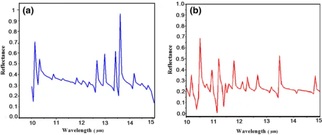
First, we consider the choice of thickness of the silver pillar. Through simulations, the reflection spectra of the structure with different thickness of the silver pillar can be found. Figure 2 plotted two sample results with the silver height of 300 nm and 150 nm for the dielectric thickness of 80 nm.
Figure 2 shows that there are many resonance peaks due to the Fabry–Perot resonator and the dips almost close to zero, and the strongest resonance peak exists at the wavelength approaches 13,800 nm. The presence of different resonance peaks attests that the system exhibits very strong response when stimulated near those frequen-cies, and is effective for reflection antenna applications. We found it a good choice for the silver nanopillar thickness to be 300 nm.
To show the performance of the antenna, the radia-tion pattern, in dB scale, at the resonant wavelength of
(5) D(𝜃, 𝜑) = P∕Pt, (6) 𝜂e= Prad∕Pin, (7) 𝜂B= 𝛺MB∕𝛺A, (8) G = 𝜂eD, (9) 𝛺A= 𝜋 ∫ 0 2𝜋 ∫ 0 p sin 𝜃d𝜃d𝜑, (10) p = ||E(r, 𝜃, 𝜑)∕Emax||2,
13,800 nm and for the thickness of the dielectric layer (tD) of 80 nm are plotted, as shown in Fig. 3a for V = 1 V and Fig. 3b for V = 4 V. From Fig. 3 we can see that the radiation pattern has high directivity.
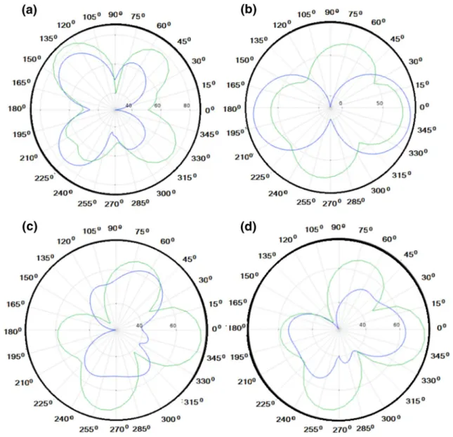
Now we study the influence of the voltage applied on the BTO layer. By changing the applied voltage, a variation of the refractive index of the BTO is obtained, as given by Eq. (4). This effect in turn produces a change in the angle of irradiation of the principal beam as shown in Fig. 4, where we have plotted the radiation patterns for the voltage of
V = 1 V (a), 2 V (b), 3 V (c), and 4 V (d).
From Fig. 4 we can see that the directivity is changed by the applied voltage, showing a directivity tunability by voltage. The presence of the larger lobe indicates that the energy is mainly radiated in one direction. In Fig. 4 we reported the radiation patterns in the Azimuth (in green color) and Elevation plane (in blue color), confirming the
typical characteristics of a directional antenna and its angle steerability.
It has been studied the optical plasmon response of the nanoantenna by varying the dielectric thickness and the height of the device maintaining V = 4 V and λ = 13,800 nm. The results obtained are shown in Table 1 for the variation of the dielectric thickness; in Table 2 for the variation of the height of nanopillars. The analysis confirms that the radia-tion pattern of the considered antenna is highly direcradia-tion sensitive to the parameters of the structure. The result in Table 1 is not explicitly predicted by Eqs. (1) and (2) which correspond to a reflection metal grating, while in the pro-posed structure, the waves meet with the nano particles, the EO dielectric layer, and the metal substrate, resulting an equivalent change in the grating constant in Eqs. (1) and (2), and thus a change in the direction of the reflected beam. The result in Table 2 presents qualitative support to
Fig. 2 Reflectance for dielectric thickness of 80 nm with silver nanopillar height of 300 nm (a), and 150 nm (b) for V = 4 V
Eqs. (1) and (2) that the radiation direction is related to the grating constant or lattice constant.
A more detailed study on the directivity tunability by voltage is indicated in Fig. 5 where θ is the beam angle of the radiation pattern in the relation indicated in Eqs. (1) and (2). From Fig. 5 we can calculate the angle tuning sen-sitivity ξ = dθ/dV, and we can observe the polar coordinate system, verifying qualitatively that there is a high tuning sensitivity for the voltage tuning in the range from 2.75 to 3 V.
The performance of antennae can be deduced from the analysis of their reflection characteristics [44].
The above analysis is done based on the field of a unit cell. Considering the unit cell number cannot be infinite in practical devices, we also calculate the directional
Fig. 4 Azimuth (green) and Elevation (blue) plane of directional radiations for the applied voltage of V = 1 V (a), 2 V (b), 3 V (c), and 4 V (d),
for td = 80 nm and λ = 13,800 nm
Table 1 Main beam direction versus the dielectric thickness
td/nm 60 70 80 90 100
θmain/deg 145 150 235 130 35
Table 2 Main beam direction versus the height
w/nm 320 325 300 335 340
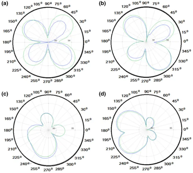
radiations of an antenna with a 5 × 5 unit cell. The direc-tional radiation patterns are shown in Fig. 6 for the voltage of V = 1 V (a), 2 V (b), 3 V (c) and 4 V (d). With the results
demonstrating the radiation-direction steerability of the device, however, additional lobe in each case is obtained in Fig. 6. This shows that the finite array structure has some differences from an infinite array structure because there is a limited-size effect in finite size devices.
With the help of the Friis Transmission Equation, we can calculate the power received from the antenna placed at distance R from the antenna operating at frequency f. We assume that the gains of the antennae GT and GR are known and the receiving antenna is in the far field of the transmitting antenna.
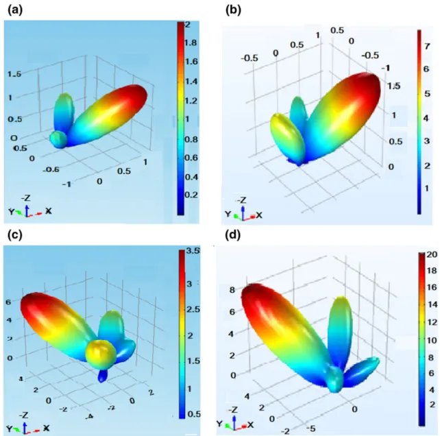
For a detailed analysis of the model’s performances, the directivity and gain for an antenna with 4 × 4 unit cells and 5 × 5 unit cells were determined.
The results reported, in dB scale, in Fig. 7 for 4 × 4 unit cells (a, b) and 5 × 5 unit cells (c, d) show that the array with a greater number of sub antennae has better perfor-mances with the gain increased from 7 to 20 dB.
Fig. 5 Beam angle tuning by voltage with a step of 0.25
Fig. 6 Azimuth (green) and Elevation (blue) plane of directional radiations for the applied voltage of V = 1 V (a), 2 V (b), 3 V (c) and 4 V (d), for
It is demonstrated by the above results that the structure proposed can serve as a voltage-controlled radiation-angle steerable antenna. Also, the simulation verified the mecha-nism of directivity tunability predicted by Eqs. (1) and (2).
More interesting, the antenna radiation-direction can be tuned by simply varying one applied voltage, while in conventional systems, complicated rotating structures or hundreds of phase-shifting units are required.
4 Conclusion
In this paper, we have proposed and verified that a structure constituted by silver nano-pillars and silver substrate with the insertion of BTO as a dielectric is a promising solution for making a steerable antenna. The results obtained by FEM simulation tool have shown
Fig. 7 Antenna with an Ag layer substrate: directivity (a) and gain
(b) from the finite structure of 4 × 4 unit cells, and directivity (c) and gain (d) from the finite structure of 5 × 5 unit cells, for td = 80 nm
and λ = 13,800 nm. The applied voltage is V = 4V and the incident angle is θ = 90°
good performances in the gain and directivity of the antenna. By a single control voltage applied on a thin EO layer, one can obtain an effect of phase-control array antennae with complicated voltage-control system. It is discussed that the joint action of the plasmon surface waves and the EO layer in the structure leads to the single-voltage steering angle of its radiation directivity. The proposed nanoantenna can find applications in bio-logic sensors, microscopy, spectroscopy, energy transfer, wireless connection in and among chips, light extracts from single photon source and sub-wavelength sized lasers, micro radar systems for micro robots or subma-rines used inside human body systems for navigation in the veins or arteries, and compensation of fabrication errors. More interesting, the antenna steerability can be tuned without requiring complicated rotating structures or hundreds of phase-shifting units.
Acknowledgements This work is supported by the NSFC (Grant Nos:
61275043, 61307048, 60877034 and 61605128), GDNSF (Grant Nos: 2017A030310455), and SZSF (Grant Nos: JCYJ20170302151033006, 20180123).
Compliance with ethical standards
Conflict of interest The authors have confirmed this manuscript has
no conflict of interest.
References
1. Gramotnev DK, Bozhevolnyi SI (2010) Plasmonics beyond the diffraction limit. Nat Photon 4:83–91
2. Tao H, Padilla WJ, Zhang X, Averitt RD (2011) Recent progress in electromagnetic metamaterial devices for terahertz applica-tions. IEEE J Sel Top Quant Electron 17:92–101
3. Boharedway P, Deutsch B, Novotny L (2009) Optical antennae. Adv Opt Photon 1:438–483
4. Yu N, Genevet P, Kats MA, Aieta F, Tetienne JP, Capasso F, Gaburro Z (2011) Light propagation with phase discontinuities: general-ized laws of reflection and refraction. Science 334:333–337 5. Deng ZL, Zhang S, Wang GP (2016) A facile grating approach
towards broadband, wide-angle and high-efficiency holo-graphic metasurfaces. Nanoscale 8:1588–1594
6. Deng ZL, Zhang S, Wang GP (2016) Wide-angled off-axis achro-matic metasurfaces for visible light. Opt Expr 24:23118–23128 7. Khorasaninejad M, Chen WT, Devlin RC, Oh J, Zhu AY, Capasso
F (2016) Metalenses at visible wavelengths: diffraction-limited focusing and subwavelength resolution imaging. Science 352:1190–1194
8. Deng ZL, Li G (2017) Metasurface optical holography. Mat Today Phys 3:16–32
9. Zheng G, Mühlenbernd H, Kenney M, Li G, Zentgraf T, Zhang S (2015) Metasurface holograms reaching 80% efficiency. Nat Nanotechnol 10:308–312
10. Sheng Z, Varadan V (2006) Effect of substrate dielectric proper-ties and tunable metamaterials. IEEE Antennas Propag Soc Int Sympos. https ://doi.org/10.1109/APS.2006.17116 35
11. Gurbatov S, Vitrik O, Kulchin Y, Kuchmizhak A (2018) Mapping the refractive index with single plasmonic antennae. Sci Rep 8, Art No. 386
12. Arslamagic S, Ziolkowski RW (2018) Highly subwavelength, superdirective cylindrical nanoantenna. Phys Rev Lett 120, Art No. 237401
13. Turpin JP, Bossard JA, Morgan KL, Werner DH, Werner PL (2014) Reconfigurable and tunable metamaterials: review of theory and application. Int J Ant Propag Art No. 429837. https ://doi. org/10.1155/2014/42983 7
14. Krasnok A, Li S, Lepeshov S, Savelev R, Boranov DG, Alù A (2018) All optical switching and unidirectional plasmon launching non linear dielectric nanoantennae. Phys Rev Appl 9, Art No. 014015 15. Lester M, Skigin DC (2011) An optical nanoantennae made of
plasmonic chain resonators. J Opt 13, Art No. 035105
16. Guo R, Decker M, Setzpfandt F, Staude I, Neshev DN, Kivshar YS (2015) Plasmonic Fano nanoantennae for on-chip separation of wavelength-encoded optical signals. Nano Lett 15:3324–3328 17. Taminiau TH, Stefani FD, Van Hulst NF (2008) Enhanced
direc-tional excitation and emission of single emitters by a nano-optical Yagi-Uda antennae. Opt Expr 16:10858–10866 18. Mesch M, Weiss T, Schaferling M, Hentschel M, Hegde RS,
Gies-sen H (2018) Highly Gies-sensitive refractive index Gies-sensor with plas-monic nanoantennae-utilization of optimal spectral detuning of Fano resonances. ACS Sens 3:960–966
19. Voskin A, Bohn J, Chong KE, Bucher T, Zilk M, Choi DY, Neshev DN, Kisvhar YS, Pertsch T, Staude I (2018) Directional and spec-tral shaping of light emission with Mie-resonant silicon nano-antennae arrays. ACS Photon 5:1359–1364
20. Laible F, Gollmer DA, Dickrenter S, Khen DP, Fleischer M (2018) Continous reversible tuning of the gap size and plasmonic cou-pling of bow tie nanoantennae on flexible substrates. Nanoscale 10:14915–14922
21. Roh S, Chung T, Lee B (2010) Overview of plasmonic sensors and their design methods. In: Proceedings SPIE 7853, Advanced sensor systems and applications IV, 785303. https ://doi. org/10.1117/12.86935 7
22. Yang CY, Yang JH, Yang ZY, Xhont ZX, Babichevol VE, Chen KP (2018) Nonradiating silicon nanoantennae metasurfaces as nar-rowband absorbers. ACS Photon 5:2596–2601
23. Novotny L, Stranick SJ (2006) Near-field optical microscopy and spectroscopy with pointed probes. Ann Rev Phys Chem 57:303–331
24. Schuller A, Taubner T, Brongersma ML (2009) Optical antennae thermal emitters. Nat Photon 3:658–661
25. Atwater HA, Polman A (2010) Plasmonics for improved photo-voltaic devices. Nat Mater 9:205–213
26. Li X, Choy WCH, Huo L, Xie F, Sha WE, Ding B, Guo X, Li Y, Hou J, You J, Yang Y (2012) Dual plasmonic nanostructures for high per-formance inverted organic solar cells. Adv Mater 24:3046–3052 27. Alu A, Engheta N (2010) Wireless at the nanoscale: optical inter-connects using matched nanoantennae. Phys Rev Lett 104, Art No. 213902
28. Ciftcioglu B, Berman R, Zhang J, Darling Z, Wang S, Hu J, Xue J, Garg A, Savidis JM, Moore D, Huang DM (2011) A 3-D integrated intrachip free-space optical interconnect formany- core chip. IEEE Photon Technol Lett 23:164–166
29. Curto AG, Volpe G, Taminiau TH, Kreuzer MP, Quidant R, Van Hulst NF (2010) Unidirectional emission of a quantum dot coupled to a nanoantennae. Science 329:930–933
30. Kosako T, Kadoya Y, Hofmann HF (2010) Directional control of light by a nano-optical Yagi-Uda antennae. Nat Photon 4:312–315
31. Moghadam NN, Farhadi H, Bengtsson M (2016) An energy effi-cient communication technique for medical implants/micro robots. In: 2016 10th international symposium on medical
information and communication technology (ISMICT), 10th ISMICT, https ://doi.org/10.1109/ISMIC T.2016.74988 87
32. Sitti M, Ceylan H, Hu W, Giltinan J, Turan M, Yim S, Diller E (2015) Biomedical applications of untethered mobile milli/microrobots. Proc IEEE Inst Electr Electron Eng 103:205–224. https ://ieeex plore .ieee.org/docum ent/70670 29
33. Munarizz J, Malishev A, Malishev VA, Knoester J (2013) Opti-cal nanoantennae with tunable radiation patterns. Nano Lett 13:444–450
34. Yi F, Shin E, Zhu A, Zhu H, Reed J, Cubuken E (2013) Voltage tun-ing of plasmonic absorber by indium tin oxide. Appl Phys Lett 102, Art No. 22102
35. Sievenpiper DF, Schaffner JH, Song HJ, Loo RY, Tangonan G (2003) Two-dimensional beam steering using an electrically tun-able impedance surface. IEEE Trans Ant Propag 51:2713–2722 36. Hashemi MRM, Yang S-H, Wang T, Sepúlveda N, Jarrahi M (2016)
Electronically-controlled beam steering through vanadium dioxide metasurfaces. Sci Rep 6, Art No. 35439
37. Burokur SN, Ourir A, Lustrac A, Yahiaoui R (2012) Metasur-faces for high directivity antenna applications in metamate-rials. In: Jiang X-Y (ed) Intech Open, pp 533–556. https ://doi. org/10.5772/35845
38. Torres VL (2014) Plasmonic and metamaterials at terahertz frequencies. Thesis, UPNA. http://acade mica-e.unava rra.es/ bitst ream/handl e/2454/18263 /Tesis %20Tor res%2cVic tor%20 SA%20ma.pdf?isAll owed=y&seque nce=1
39. Kreibig U, Zacharias P (1970) Surface plasma resonances in small special silver and gold particles. Z Phys 231:128–143
40. Bibbò L, Liu Q, Lin M, Wang Q, Ouyang Z (2017) Tunable per-fect absorber for biosensing. In: 10th global symposium on millimeter waves Hong Kong, https ://doi.org/10.1109/ GSMM.2017.79703 18
41. Abel S, Ortmann E, Eltes F, Messner A, Castera P, Wagner T, Urbo-nas D, Rosa A, Gutierrez AM, Tulli D, Ma P, Baeuerle B, Josten A, Heni W, Caimi D, Czornomaz L, Demkov AA, Leuthold J, Sanchis P, Fompeyrine J (2018) Large Pockels effect in micro nanostruc-tured barium titanate integrated on silicon. Nat Mat 18:42–47 42. Bibbò L, Liu Q, Khan K, Yadav A, Elshahat S, Deng ZL, Ouyang Z
(2019) High speed amplitude modulator with a high modulation index based on a plasmonic resonant tunable metasurface. Appl Opt 58:2687–2694. https ://doi.org/10.1364/AO.58.00268 7
43. Dicken MJ, Sweatlock LA, Pacifici D, Lezec J, Bhattacharya Atwa-ter HA (2008) Electrooptic modulation in thin film barium titan-ate plasmonic interferometer. Nano Lett 8:4048–4052 44. Yifat Y, Iluz Z, Eitan M, Friedler I, Hanein Y, Boag A, Scheuer J
(2012) Quantifying the radiation efficiency of nano antennae. Appl Phys Lett 100, Art No. 111113
Publisher’s Note Springer Nature remains neutral with regard to