www.mdpi.com/journal/coatings
Supplementary Materials: Chemical Solution
Deposition of YBCO Films with Gd Excess
Valentina Pinto 1, Angelo Vannozzi 1, Achille Angrisani Armenio 1, Francesco Rizzo 1, Andrea
Masi 2, Antonino Santoni 3, Alexander Meledin 4,5, Fabrizio Mario Ferrarese 1, Silvia Orlanducci 6
and Giuseppe Celentano 1,*
1 Superconductivity Section, FSN-COND, ENEA, Via Enrico Fermi 45, Frascati, 00044 Rome, Italy;
[email protected] (V.P.); [email protected] (A.V.); [email protected] (A.A.A.); [email protected] (F.R.); [email protected] (F.M.F.)
2 Engineering Department, Roma Tre University, Via Vito Volterra 62, 00146 Rome, Italy;
3 FSN-TECFIS-MNF, ENEA, v. E. Fermi 45, Frascati, 00044 Rome, Italy; [email protected] 4 Central Facility for Electron Microscopy, RWTH Aachen University, 52074 Aachen, Germany;
5 Ernst Ruska-Centre for Microscopy and Spectroscopy with Electrons (ER-C), Forschungszentrum Jülich
GmbH, 52428 Jülich, Germany
6 Department of Chemical Sciences and Technologies, Tor Vergata University, Via della Ricerca Scientifica,
00133 Rome, Italy; [email protected] * Correspondence: [email protected]
(a) (b)
(c)
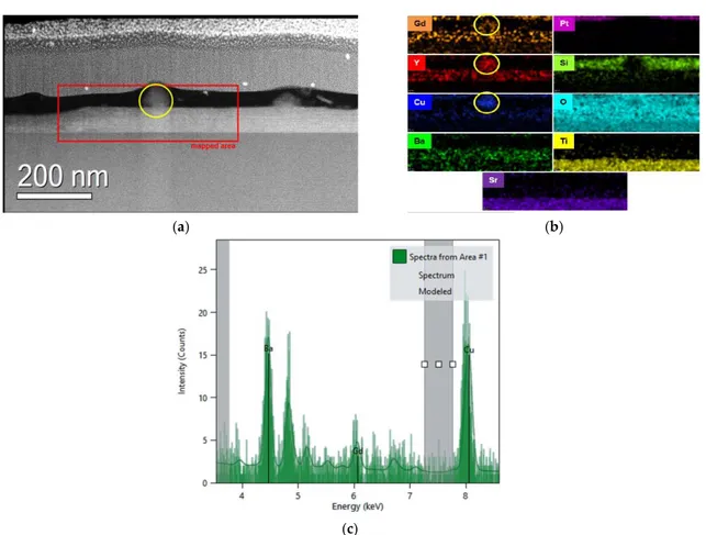
Figure S1. TEM overview of YBCO-Gd 5% film deposited with standard process. Cross-section view: HAADF STEM image showing the mapped area together with elemental Y, Gd, Ba, and Cu EDX maps confirming a uniform Y and Gd distribution. (a) HAADF STEM overview of YBCO-Gd 5% film deposited by standard process YBCO layer morphology. The (Gd,Y)2Cu2O5 precipitate is highlighted by yellow circle. The area of EDX mapping is shown by red rectangle (b) elemental Gd, Pt, Y, Si, Cu, O, Ba, Ti and Sr EDX maps confirm a uniform Y and Gd distribution. (c) EDX spectrum from YBCO layer area proofs Gd presence in the layer.
2 of 2
© 2020 by the authors. Licensee MDPI, Basel, Switzerland. This article is an open access article distributed under the terms and conditions of the Creative Commons Attribution (CC BY) license (http://creativecommons.org/licenses/by/4.0/).