Procedia Engineering 168 ( 2016 ) 313 – 316
Available online at www.sciencedirect.com
1877-7058 © 2016 The Authors. Published by Elsevier Ltd. This is an open access article under the CC BY-NC-ND license (http://creativecommons.org/licenses/by-nc-nd/4.0/).
Peer-review under responsibility of the organizing committee of the 30th Eurosensors Conference doi: 10.1016/j.proeng.2016.11.204
ScienceDirect
30th Eurosensors Conference, EUROSENSORS 2016
Titanium dioxide nanostructures chemical sensor
A. Bertuna
a*, E. Comini
a, N. Poli
a, D. Zappa
a, G. Sberveglieri
aaSENSOR Laboratory University of Brescia and CNR-INO, Via D. Valotti 9, 25133 Brescia, Italy
Abstract
Titanium dioxide (TiO2) nanostructures were grown directly on the sensitive area of the transducer. A titanium
thin film was deposited on 2 · 2 mm2alumina substrates by RF magnetron sputtering and hydrothermal method
was used to achieve TiO2. This method is characterized by the use of different solutions (KOH, NaOH), a not
stirred pressure reactor and a heating system. As-prepared samples require an acid treatment followed by a calcination step to obtain pure TiO2nanostructures. The nanostructured morphology was confirmed by a scanning
electron microscope (SEM) and their structural properties were investigated by RAMAN spectroscopy. Obtained samples were used as gas sensors, and their behaviour towards several gaseous species was analysed in a wide range of working temperatures. Measurements were carried out in a test chamber, investigating the change in the electrical conductance due to the surrounding atmosphere.
© 2016 The Authors. Published by Elsevier Ltd.
Peer-review under responsibility of the organizing committee of the 30th Eurosensors Conference.
Keywords: Titanium dioxide; nanostructures; hydrothermal treatment; chemical sensor; Raman spectroscopy
1. Introduction
Titanium dioxide is widely used in several technological fields such as photo-catalysis, hydrogen production by water splitting, solar cells, gas sensors and biological applications. It can also be used for the preparation of paper, plastic, toothpaste and in paints as withe pigment. TiO2 is intensely studied thanks to its numerous characteristics
such as non-toxicity, chemical stability and electrical properties [1]. Nowadays titanium dioxide and other metal oxides in the form of nanostructures are used, for their thermal, electric, mechanic, optics properties, in many fields, like sensors, biomedical, solar cell, safety, energy storage and in many other applications [2]. Furthermore,
* Corresponding author. Tel.: +39-030-371-5873; fax: +39-030-209-1271.
E-mail address: [email protected]
© 2016 The Authors. Published by Elsevier Ltd. This is an open access article under the CC BY-NC-ND license (http://creativecommons.org/licenses/by-nc-nd/4.0/).
314 A. Bertuna et al. / Procedia Engineering 168 ( 2016 ) 313 – 316
in one-dimensional structures the surface/volume ratio increases and the crystallinity is high. These two factors make them more sensitive in the detection of target gases [3]. One of the most used techniques to growth nanostructures is the hydrothermal treatment, thanks to the possibility to work at low temperatures and to obtain a homogeneous growth [1, 4].
In this work, we present different types of TiO2 nanostructures grown directly on the sensitive area of transducers
to avoid transferring of nanostructures after the growth in order to improve mechanical and electrical stability of devices. The technique used to growth titanium dioxide nanostructures was hydrothermal treatment. This work shows also the functional properties of chemical sensors based on as prepared TiO2 nanostructures.
2. Experimental
Alumina 2 · 2 mm2 substrates were ultrasonically cleaned in acetone for 15 minutes in order to eliminate all the
compounds on the surface that can interact during the metal deposition, contaminating it. Afterwards substrates were dried under a flow of synthetic air. Once finished cleaning, RF magnetron sputtering was used to deposit a film of metallic titanium of 100 nm. An electrical power of 75 W was applied to the target, the argon flow was set to 7 sccm and the duration of deposition was 24 minutes. A better adhesion of the film to alumina substrate was guaranteed by heating samples at 100 °C during the deposition.
The growth of several types of nanostructures was performed with hydrothermal treatment using two different hydroxide solution, KOH and NaOH, and different working conditions. Inside a not stirred pressure reactor, solution and samples were added. Thanks to a heating system it was possible change the working temperature. We obtained three different kinds of nanostructures: nanosponge (KOH 0.12 M, 160 °C, 6 hours), nanoflakes (NaOH 0.1 M, 170 °C, 25 hours) and a mix of nanosponge and nanoflakes, which will be defined hereafter nanomix (KOH 0.05 M, 170 °C, 25 hours). All the samples after the hydrothermal treatment were treated in acid (HCl 0.1 M, 1 o hours) and annealed in air in two steps, at first at 50 °C for 1 hour and than at 400 °C for 2 hours.
Samples surface was investigated by a field emission scanning electron microscope (FE-SEM) LEO 1525 operated at 5 kV beam voltage, in order to analyze the morphology of as prepared samples.
Raman spectroscopy was performed on as obtained nanostructures in order to investigated their structural properties. The Raman system is composed by a fibre-coupled confocal optical microscope (HORIBA), a He-Cd blue laser (442 nm), a HORIBA monochromator iHR320 and a Peltier-cooled Synapse CCD.
To fabricate chemical sensors, platinum interdigitated contacts and platinum heating element were deposited by DC Magnetron sputtering (75 W, 7 sccm of argon, 300 °C, 20 minutes for both the depositions) on the top of nanostructures and on the backside of alumina, respectively. Thanks to gold wires, substrates were bonded to a TO case, then devices were placed in a stainless-steel homemade test chamber, with a volume of 1 L, and they were exposed to several gaseous species (carbon monoxide, ethanol, methanol, acetone and hydrogen). Measures were carried out using three different concentration for each gas and setting relative humidity at 40%@20°C. The working temperature of each device was changed from 300 °C to 600 °C and the power applied to each sensor was 1 V.
The changing in the value of electrical conductance gives information about the ability of sensors to detect the different gases injected in the test chamber. The following laws, for oxidizing (1) and reducing (2) gases regulate this variation (in case of n-type metal oxide).
Re sponse
=
G
air−Ggas
G
gas (1)Re sponse
=
G
gas−Gair
315
A. Bertuna et al. / Procedia Engineering 168 ( 2016 ) 313 – 316
3. Results
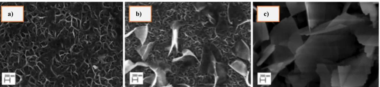
The different working conditions (solution, molarity, temperature and time) of the hydrothermal process have resulted in the growth of three different types of nanostructures. Figure 1 shows SEM images of samples morphology: nanosponge (a), nanomix (b) and nanoflakes (c).
Fig. 1. Morphology of different TiO2 nanostructures at 50 k level: nanosponge (a), nanomix (b) and nanoflakes (c).
RAMAN spectroscopy allows us to check the crystalline phase of samples. Figure 2 shows the spectrum of nanostructures prepared in KOH solution (blue) compared with the spectrum of titania in the form of rutile (yellow) and alumina spectrum (green). Green and yellow arrows underline alumina and titania (rutile) picks, respectively, on prepared nanostructures spectrum.
Fig. 2. Raman spectra of TiO2 nanostructures (blue) titania in the form of rutile (yellow) and alumina (green).
TiO2 nanostructures based gas sensors were tested towards different target gases, like carbon monoxide,
acetone, ethanol, methanol and hydrogen. In this work are shown the dynamic response of a device (nanosponge based gas sensor) towards hydrogen at 600 °C, the sensor response in the temperatures range towards 500 ppm of H2 and calibration curves at 600 °C towards the same gas (Figure 3 a, b, c, respectively).
The dynamic response shows the increment in the conductance value in correspondence of gas injections (100, 250, 500 ppm), typical of n-type metal oxide exposed to reducing gases (as shown by equation (2) in the experimental part). Figure 3b underlines how the sensor response changes in function of the temperature and it highlights the optimal working temperature (600 °C). The detection limits for the device was calculated
316 A. Bertuna et al. / Procedia Engineering 168 ( 2016 ) 313 – 316
considering minimum response as 1 and its value is 2.34 ppm.
Fig. 3. Dynamic response of prepared nanostructures to H2 @600 °C RH = 40% (a); Response of prepared nanostructures at different temperatures to 500 ppm of H2 (b); Calibration curve @ 600 °C (c).
4. Conclusions
Hydrothermal technique is used to growth three different types of nanostructures, thanks to different working conditions and two different solution (KOH and NaOH), on the active transducer to improve mechanical and electrical stability. As obtained devices were tested in a wide range of temperatures towards different hydrogen concentrations. The optimal working temperature is around 600 °C for a relative humidity of 40% towards 500 ppm of hydrogen. Further tests will be carried out in order to compare each other the different device types and to understand if the three morphologies show the same response towards different gaseous species.
Acknowledgements
This work was supported by the European Community’s 7th Framework Programme, under the grant agreement n° 611887 “MSP: Multi Sensor Platform for Smart Building Management”.
References
[1] J S. Bagheri, Z. A. M. Hir, A. T. Yousefi, et al., Progress on mesoporous titanium dioxide: Synthesis, modification and applications, Micropor. Mesopor. Mat. 218 (2015) 206-222.
[2] Y.N. Xia, P.D. Yang, Y.G. Sun, et al., One-dimensional nanostructures: synthesis, characterization, and applications, Adv. Mat. 15 (2003) 353-389.
[3] J. Bai, et al., Titanium dioxide nanomaterials for sensor applications, Chem. Rev. 114 (2014) 10131-10176.
[4] K. Byrappa, T. Adschiri, Hydrothermal technology for nanotechnology, Prog. Cryst. Growth. Charact. Mater. 53 (2007) 117-166.
a b