Politecnico di Milano
Facolt`
a di Ingegneria dei Processi Industriali
Degree in Materials Engineering and Nanotechnology
Atomic Layer Deposition of
Ferroelectric Complex
Oxide Thin Films
Advisor Dr. Jonathan E. Spanier
Drexel University, Philadelphia, Pennsylvania, United States of America
Co-Advisor Dr. Carlo S. Casari
Politecnico di Milano, Milano, Italia
A Thesis
Submitted to the Faculty in
Partial Fulfillment
of the Requirements for the Degree of
Master of Science
by:
Brian R. Beatty
Matricola: 780703© Copyright July 2012
For my parents and everyone else who helped out along the way...
Contents
List of Figures viii
List of Tables xi Acknowledgements xiii Abstract xvii Sommario xix 1 Introduction 1 1.1 Project Scope . . . 2 2 Lead Titanate 5 2.1 Structure . . . 5 2.1.1 Effect of Temperature . . . 5 2.2 Ferroelectricity . . . 6 3 Synthesis Methods 9 3.1 Sol-Gel Processing . . . 9
3.2 Metallorganic Chemical Vapor Deposition . . . 10
3.3 Atomic Layer Deposition . . . 11
4 Thin Film Growth 15 4.1 Precursor Selection . . . 15 4.1.1 Titanium Source . . . 15 4.1.2 Lead Source . . . 15 4.1.3 Oxidizer . . . 16 4.2 Substrate Preparation . . . 16 4.2.1 Si(100) . . . 16 4.2.2 Platinized Si(100) . . . 17
4.2.3 Single Crystal STO(100) . . . 17
4.3 Deposition Parameters . . . 18
4.3.1 Growth Temperature . . . 18
4.3.2 Precursor Dosage . . . 19
4.3.3 Purge Time . . . 19
4.3.4 Exposure Time . . . 20
4.4 Post-Deposition Annealing . . . 20
4.4.1 Oven Annealing . . . 20
4.4.2 Rapid Thermal Annealing . . . 21
5 Material Characterization 23 5.1 Thermal Analysis . . . 23
5.1.1 Thermogravimetric Analysis . . . 23
5.1.2 Differential Scanning Calorimetry . . . 23
5.2 Thin Film Characterization . . . 25
5.2.1 Variable Angle Spectroscopic Ellipsometry . . . 25
5.3 Compositional Analysis. . . 28
5.3.1 Energy-Dispersive X-Ray Spectroscopy . . . 28
5.3.2 X-Ray Fluorescence Spectroscopy . . . 28
5.4 Phase Identification . . . 29
5.4.1 X-Ray Diffraction . . . 29
6 Analysis Methods 33 6.1 Thermal Analysis . . . 33
6.1.1 Thermogravimetric Analysis . . . 33
6.1.2 Differential Scanning Calorimetry . . . 33
6.2 VASE and Modeling . . . 33
6.2.1 Data Collection . . . 34
6.2.2 Model Definition . . . 35
6.2.3 Analysis Procedure . . . 36
6.3 Composition Analysis . . . 39
6.3.1 X-Ray Fluorescence Spectroscopy . . . 40
6.4 X-Ray Diffraction . . . 40
7 Results 43 7.1 Thermal Analysis . . . 43
7.1.1 Thermogravimetric Analysis . . . 43
7.1.2 Differential Scanning Calorimetry . . . 45
7.2 List of Samples . . . 49
7.3 Ellipsometry . . . 50
7.4 Composition . . . 52
8 Conclusions 57
8.1 Future Work. . . 58
Bibliography 59 A Supplemental Information 67 A.1 List of Chemicals . . . 67
A.2 ALD Reactor Diagram . . . 68
A.3 Composition Results . . . 69
List of Figures
2.1 Crystal Structures of Perovskites and PbTiO3 . . . 6
2.2 Energy vs. Polarization Plots for FE and PE Materials . . . 7
2.3 Polarization vs. Applied Field Plots for FE and PE Materials . 7 3.1 Illustration of Example ALD Cycle . . . 12
5.1 T.A. Instruments, inc. Instrumentation . . . 24
(a) Q50 TGA . . . 24
(b) Q2000 DSC . . . 24
5.2 Ellipsometric Beam Path and Modeling Parameters . . . 25
5.3 J.A. Woollam M-2000U Ellipsometer . . . 27
5.4 Illustration of EDXS principle . . . 29
5.5 Illustration of Bragg’s Law . . . 30
(a) Constructive Interference. . . 30
(b) Destructive Interference . . . 30
5.6 Rigaku SmartLab XRD. . . 31
6.1 Graphical Schematic of VASE Model . . . 36
6.2 Preferred Phase vs. Stoichiometric Ratio . . . 39
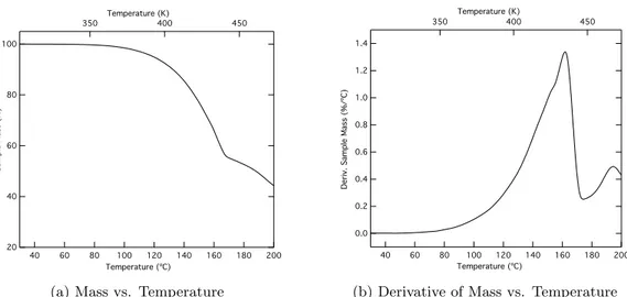
7.1 TGA Results for Pb(HFAc)2 Precursor . . . 44
(a) Mass vs. Temperature . . . 44
(b) Derivative of Mass vs. Temperature . . . 44
7.2 TGA Results for Pb(HFAc)2 Precursor . . . 45
(a) Mass vs. Temperature . . . 45
(b) Derivative of Mass vs. Temperature . . . 45
7.3 Constant Temperature TGA Experiments . . . 46
(a) Pb(HFAc)2 . . . 46
(b) Pb(TMHD)2 . . . 46
7.4 DSC Results of Pb(HFAc)2 . . . 47
7.5 DSC Results of Pb(TMHD)2 . . . 48
7.6 Film Thicknesses vs. Deposition Cycles . . . 51
7.7 XRD Scan of #0 on Si . . . 54
7.8 XRD Scan of #23 on Pt . . . 55
7.9 XRD Scan of #20 on Pt-SI . . . 56
7.10 XRD Scan of #28 on STO . . . 56
A.1 Cambridge NanoTech, inc. S100 ALD System . . . 68
(a) Photograph . . . 68
(b) Schematic Diagram . . . 68
A.2 XRF Spectrum of PTO #0 . . . 69
A.3 XRF Spectrum of PTO #20 on Pt-Si . . . 69
A.4 Results of Ellipsometry on Sample #0 . . . 72
(a) Psi vs. Wavelength . . . 72
(b) Delta vs. Wavelength. . . 72
(c) n, k vs. Photon Energy . . . 72
A.5 Results of Tauc Analysis on Sample #0 . . . 73
(a) Absorption (α) vs. Photon Energy . . . 73
(b) Tauc (α2E2 ph) vs. Photon Energy . . . 73
A.6 Results of Ellipsometry on Sample #20 on Platinized Silicon . . 74
(a) Psi vs. Wavelength . . . 74
(b) Delta vs. Wavelength. . . 74
(c) n, k vs. Photon Energy . . . 74
A.7 Results of Tauc Analysis on Sample #20 on Platinized Silicon . 75 (a) Absorption (α) vs. Photon Energy . . . 75
(b) Tauc (α2E2 ph) vs. Photon Energy . . . 75
A.8 Results of Ellipsometry on Sample #28 on STO . . . 76
(a) Psi vs. Wavelength . . . 76
(b) Delta vs. Wavelength. . . 76
(c) n, k vs. Photon Energy . . . 76
A.9 Results of Tauc Analysis on Sample #28 on STO . . . 77
(a) Absorption (α) vs. Photon Energy . . . 77
(b) Tauc (α2E2 ph) vs. Photon Energy . . . 77
List of Tables
7.1 List of Samples . . . 49
7.2 Sample Thicknesses and Growth Rates . . . 51
7.3 XRF Calculated Compositions . . . 53
A.1 List of Compounds . . . 67
A.2 PTO #0 Ellipsometric Model Variables . . . 70
A.3 Calculated Band Gap Energies. . . 70
A.4 PTO #20 Ellipsometric Model Variables . . . 71
A.5 PTO #28 Ellipsometric Model Variables . . . 71
Acknowledgements
I would like to start by acknowledging Dr. Jonathan Spanier for all of the all of the guidance that he has given to me over the course of my tenure at Drexel University. Allowing me to enter into the research side of school as a young freshman with stars in his eyes was undeniably one of the defining points in my academic career. The variety of skills I have been able to learn while working with him, and of course all of the members of his extremely talented group, are sure to prove to be invaluable during the next stages of life after Drexel. While I learned plenty of facts and received valuable training in an incredible range of technical equipment, what really stands out is the manner in which I was taught how to think. How to think about puzzling results that didn’t quite add up evenly. How best to plan experiments to maximize the data obtained from it. Analyzing the remnants from when things went wrong, and figuring out how to prevent such things from happening in the future. The researcher’s mindset is one of inquisitiveness and analysis and a drive to truly understand, and it has been of great value both in and out of the laboratory.
Another pair of honorable mentions goes to Dr. Stephen Nonnenmann and Dr. Eric Gallo. These two would act as mentors as I tried to get my feet under me in my first year or so. Always around to bounce questions off of, quick with helpful advice, and utterly filled to the brim with useful knowledge. Between these two, there was nothing that couldn’t get done or be answered in the lab. These two set me up with the knowledge and mental tools I would need to go off exploring on my own journeys into the wild seas of science. I cannot thank them enough.
Then there was the rest of the stalwart crew. Stephanie Johnson, Oren Leaffer, Terrance McGuckin, Guannan Chen, and Christopher Hawley. And I couldn’t forget my fellow undergrads Dominic Bruzzese and Michael Coster. The great conversations — especially with Oren (whom I can still count on for some useful advice about any question) even if they tended to get a little long-winded at times — that I had with these characters will be some of my best memories from my time here. Each of us had our own idiosyncrasies, but I like to think we made a fantastic team when you put us all together.
Of course, I would also like to send a heartfelt thank you to three more individuals who worked closely with my project at three very different stages. Rahul Joseph was my mentor when I first joined the lab, and it was a derivative
of his project that over time metamorphosed into the thesis sitting before you. Dr. Greg Soja was a post-doctorate fellow who worked alongside me on this project as well, and helped solve some rather difficult problems that we encountered. Last, but far from least, is Dr. Maria Sancho-Torres. She brought a bit of spark and a new point of view to the project that, again, helped sort out some problems that otherwise might have stymied me for a lot longer than they should have.
I must also thank Keith Fahnstock and Dr. Caroline Schauer for allowing me and helping me with the use of their ellipsometer. Keith in particular, for his training and just good conversation (both on and off topic) when data collection got boring. In the same vein, I must gratefully acknowledge the assistance that Dr. Amy Fahnstock and her advisor Dr. Giuseppe Palemese provided me by allowing access to their TGA and DSC instrumentation that was pivotal to the success of this project.
Of course, one does not live in a bubble, and I must thank the rest of the excellent faculty of the Materials Engineering Dept. for all of their efforts (both for their informative courses, but primarily for the discussions we had outside the classroom). I feel that I need to particularly acknowledge Dr. Steve May and Dr. Antonios Zavaliangos in this regard.
Along the lines of the opportunity I have had during this past year abroad, I would like to personally thank Dr. Carlo Casari, Politecnico di Milano, and everyone who had a hand in making the E.A.G.L.E.S. program come together. And of course the scores of crazy friends that I picked up along the way.
This has been a lot of talk already, but I personally feel I saved the most important for last. My father, Bruce, and my mother, Amy, deserve more thanks than I think they realize. For being the supports that I could fall back on, for sharing in both the little successes and the big triumphs, for always letting me talk about what I was working on (and oh the respect I have for trying to learn about it from me...), and for always pushing me to go beyond what I thought I was capable of. Mom and Dad, thank you so very much. This one’s for you guys. Now on with the show.
Abstract
Advanced technologies derive many of their capabilities from the advanced materials that they are made from. Complex oxides are a class of materials which are driving technological advancement in a host of different directions. These highly functional materials have a great variety of useful properties, which can be chosen and even engineered through careful choice of material.
Advanced materials require advanced deposition methods. Atomic layer deposition (ALD), a variant of chemical vapor deposition (CVD), is gaining more use in industry for its ability to provide ultra-high film thickness res-olution (down to 0.1 nm), capability to conformally coat three-dimensional structures, and its high uniformity across large surface areas. Additionally, ALD processes provide a possibility to improve economic and environmental viability of the process as compared to CVD by using and wasting less toxic reactants and expelling fewer nano-particulate byproducts.
ALD processes are highly mature for many binary oxides commonly used in the semiconductor industries, however processes for depositing heavy metal oxides and complex oxides — oxides containing two or more separate metallic cations — are sorely lacking in literature.
The primary focus of this work is the development of a process for
deposit-ing the complex perovskite oxide lead titanate (PbTiO3), an end group of the
lead zirconate titanate family (PbZrxTi1-xO3), which has valuable technical
ap-plications as well as serves as a template for applying this research into other material systems.
The author gratefully acknowledges the Army Research Office (ARO) for their support of this project under the funding provided by Grant # W911NF-08-1-0067.
Sommario
In this study, a method is proposed for the development of a novel ALD thin-film deposition process. This involves the identification, testing, and se-lection of precursors; analysis of growth parameters and their effects on the produced films; and in-depth ex situ characterization of prepared films via a variety of techniques.
The material under consideration is lead titanate (PTO, PbTiO3), which
is an end group of the lead zirconate titanate family (PZT, PbTi1-xZrxO3).
Lead titanate is a complex perovskite oxide, which exhibits ferroelectricity at room temperature and has a high Curie temperature at which it transitions to paraelectric behavior. Ferroelectricity is an interesting material property, as it involves a hysteretic behavior with regard to the polarization of the material. This allows the material to switch from one state to another and recall this stored polarization even without the presence of an electric field. This property has a wide variety of applications in electronics and other physical sciences.
There are a large number of potential deposition techniques for thin film structures. Some, such as sol-gel processing, work on the principles of wet chemistry and allow for the formation of films with a tightly controlled com-position. However, such techniques come with all of the drawbacks of solution based methods. Chemical vapor deposition (CVD) is another very common deposition method for thin films. It has a number of advantages, such as the ca-pability to epitaxially deposit films (which greatly improves interface quality). However, it is not easy to precisely control film thicknesses and conformally coating non-planar structures is a very difficult task.
Atomic layer deposition (ALD) is a modification on standard CVD pro-cesses. It separates the reaction between the metallic precursor and the oxidant into two half reactions. These half reactions are only capable of occurring on the surface of the substrate, as opposed to occurring in the gas phase. By sep-arating the reactions a number of important changes happen. One of the most critical, and a hallmark of an ALD deposition, is that the reaction becomes self-limiting. A half reaction can only deposit at most a single monolayer of material. This gives the incredibly high thickness resolution that can only be obtained by a very few processes. ALD is capable of resolutions down to the
angstrom level (1 ˚A = 0.1 nm). This self-limiting behavior also gives ALD some
of its other advantages, such as the ability to precisely and conformally coat
a complex three-dimensional structure with the same high resolution. This is nearly impossible with any other deposition process.
ALD precursors are more particular than those for CVD. They must be reactive with the surface and with an oxidizer, but they cannot be capable of reacting with themselves. The temperature required to activate the reaction with the surface must be lower than the temperature required to pyrolytically crack the molecule. Finally, at the end of each pair of half reactions new surface sites capable of reacting with the precursor must be repopulated with the proper ligands.
A commonly used ALD precursor for titanium is readily available: tita-nium(IV) isopropoxide. However, there is no single ideal ALD precursor for lead. Of a number of different compounds two were chosen for further
inspec-tion: bis(2,2,6,6-tetramethyl-3,5-heptanedionato) lead(II) (Pb(TMHD)2) and
lead(II) hexafluoroacetylacetonate (Pb(HFAc)2).
The two selected precursors were analyzed using thermogravimetric analysis (TGA) as well as differential scanning calorimetry (DSC). Between the two techniques it was possible to identify the regions of ideal volatility as well as a potentially viable temperature range where ALD reactions could take place.
From this analysis, it was expected that Pb(TMHD)2 would perform better in
an ALD process than Pb(HFAc)2.
A number of samples were prepared and analyzed. Variable angle spectro-scopic ellipsometry was used to measure film thicknesses and growth rates, along with some optical and electronic properties. Calibrated X-ray fluo-rescence spectroscopy (XRF) was used to obtain quantitative compositional analyses on the samples. X-ray diffraction (XRD) was used to investigate the phases present and their relative concentration in the final samples.
In concluding this study, it was found that it is possible to grow complex perovskite oxides via ALD. However obtaining crystallized samples of pure perovskite phase was non-trivial and requires more investigation to fully ac-complish. However, the study did manage to develop a valuable procedure for developing ALD processes of various materials.
Further work would include analysis of the ferroelectric behavior of the films, improving phase purity in the final samples, and extension of the method
to creating depositions for other material systems such as PbTi1-xZrxO3 or
Chapter 1
Introduction
Modern technology stands on the shoulders of modern materials, and the two are inextricably linked together. Whenever a new material or property has been discovered or engineered, applications of this new capability lie just over the horizon.
One of the hotbeds of innovation and interest in novel applications of ma-terial properties is the field of oxide chemistry. Such a seemingly simple class of materials, examples of which are two of the most abundant compounds on Earth (i.e. silica and alumina), has an incredibly rich set of capabilities de-rived from the incredible variety of potential materials. One example is the
field of high-k dielectric oxides, such as hafnium oxide (HfO2) and zirconium
oxide (ZrO2),1,2 which are allowing the semiconductor industry to produce
more capable devices while reducing power draw. Ferromagnetic and antifer-romagnetic oxides form the basis of the ubiquitous magnetic hard disk drive, advancements in deposition and microstructure control allow for the steady
increase in capacities that consumers have become accustomed to.3
The class of ferroelectric oxides comprises the family of materials that this thesis will consider. One material in particular will be the primary subject:
lead titanate (PTO, PbTiO3).4,5 Lead titanate is one end group of the lead
zir-conate titanate family of ferroelectric oxides (PZT, PbZr1-xTixO3).6 The PZT
family is of particular technical importance to many applications, especially
the PbZr0.52Ti0.48O3 form which exhibits exemplary piezoelectric, ferroelectric,
and pyroelectric behavior. PZT’s piezoelectric capabilities allow for it to be used as actuators and sensors in innumerable devices (e.g. tip actuators in AFM microscopes and transducers in ultrasound imagers).
Other applications of such materials are found when they are created as nanoscale thin films, where these capabilities are both more strongly exhibited. One of the more prevalent methods of producing nanoscale films is chemical vapor deposition (CVD), a powerful process that has been used to deposit a
vast number of material types and structures.7
However, there are disadvantages to the CVD method of film deposition. Great care must be taken to obtain highly regular film thicknesses, and the
2 Chapter 1: Introduction
method of producing most oxide films — a variation called metallorganic CVD (MOCVD) after the metallorganic compounds used as reactants — allows a significant amount of hazardous material to be released into the environment as toxic and nano-particulate byproducts.
Another deposition method, atomic layer deposition (ALD), is becoming popular in industry applications as an alternative to CVD. ALD provides the user with ultra-high resolution on film thickness, a lower operating temperature than nearly all CVD processes, amongst other features. In addition, due to the nature of the process, ALD is capable of consuming far less precursor material as well as utilizing a far larger percentage in depositing the film as
opposed to producing the types of byproducts caused by CVD.8 This makes
ALD, in situations where it can be applied, the more economical choice, as well as being more sustainable and environmentally friendly. To this end, the National Science Foundation (NSF) has awarded funding (under 2012 grant #1200940) toward the development of alternative ALD precursors, models, and processes that will attempt to provide additional improvements to the sustainability of ALD.
However, well described processes for producing ALD films of many
mate-rials have not been developed. Binary oxides (AxOy) have been explored in a
fair amount of depth,1,3,9–11 but there is less research work available covering
processes for depositing complex oxide films via ALD.
1.1
Project Scope
This thesis will cover the main steps taken in developing a thin film
depo-sition processes using ALD. In chapter 2 lead titanate as a material will be
introduced, discussing its atomic structure and some of the desirable properties that it causes the oxide to exhibit.
Chapter 3 will be devoted to a few of the commonly used methods used to
produce films of complex oxides, sol-gel and MOCVD, as well as introducing in detail the primary focus of this project: ALD as a mechanism for deposition of thin films.
Following this, chapter 4 will go into detail of the various choices and
parameters that go into the development of an ALD process. Concepts such as the choice of precursors, the various deposition parameters that must be carefully controlled and tuned to produce optimal results, and post-deposition annealing will be discussed here.
1.1: Project Scope 3
Chapter 5 will introduce and briefly discuss the topics involved in
charac-terizing the various materials to be utilized in the deposition process, as well as the various techniques used to analyze and quantify the properties of the produced samples.
Subsequently, chapter6will go into more detail of exactly how these
charac-terizations were performed, briefly mentioning various details of the standard measurement techniques as well as going into a bit more detail where analysis procedures were developed for application to this project.
In chapter 7, the details of the results and data collected from the various
measurements and experiments that were performed during this study will be presented. These results will be discussed at length, particularly focusing on how they affected the progress and choices made during the course of the project and the final results of deposited samples.
Finally, chapter 8will draw conclusions from the entirety of the work done
in the course of this project, as well as discuss possibilities for future experi-mentation and refinement of the process. A prime example of this would be to apply this research into the development of a procedure to produce films composed of the far more technically relevant PZT(52-48).
Chapter 2
Lead Titanate
2.1
Structure
Lead titanate (PbTiO3, PTO) naturally orders into the tetragonal
per-ovskite crystal structure at room temperature (figure 2.1 on the following
page). The structure can be affected by compositional changes, temperature,
or strain (primarily in thin-film systems), allowing a transition to a cubic
phase. In the perovskite crystal structure, the central cation (Ti4+ in the case
of PbTiO3) is encapsulated in a octahedral cage of anions (O2–), with the
re-maining cations (Pb2+) situated in the eight corners of the unit cell.4,5,12–18
If the material was doped (as in a mixed solid-solution), some of the cations
would be replaced with the dopant ions, for example Zr4+ would be randomly
distributed in Ti4+ sites in the PbTi1-xZrxO3 (PZT) system.4,5,12–18
2.1.1 Effect of Temperature
The transition from tetragonal to cubic perovskite is highly dependent on temperature. The critical temperature at which this transition occurs is
re-ferred to as the Curie temperature (TC). If the material cools through this
temperature, a lengthening of the ‘c’ axis of the unit cell spontaneously occurs via a first order phase transition. This creates anisotropy in the structure and allows for an anisotropic charge distribution to develop. In lead titanate this is caused by the shifting of the titanium ion, along with a slight shift of some
of the oxygen ions as well (visible in figure 2.1b on the next page). Thus, a
permanent dipole is created whose magnitude increases as the system cools
further from TC. This permanent dipole allows the system to exhibit
ferro-electricity, implying an ability to semi-permanently switch the orientation of the dipole in the material. This switching can be reversed, but this will not occur spontaneously.12,15,17,18
6 Chapter 2: Lead Titanate
Chapter 2
Fundamentals of Ferroelectricity
2.1
General
Perovskites, which can be ferroelectric materials, occur in the ABO3 formation
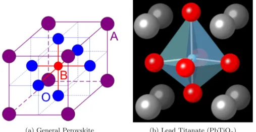
where A and B represent metals. The three oxygen atoms are located in the center of the faces of an FCC structure while one metal atom is in the center of the unit cell and the other is located at the eight corners of a tetragonal structure. Figure2.1
(from [7]) shows the perovskite structure when there is no strain applied.
Figure 2.1: Perovskite structure for functional oxide ABO3.
5
(a) General Perovskite (b) Lead Titanate (PbTiO3)
Figure 2.1: The perovskite (ABO3) crystal structure.
(a) The general structure of perovskite oxides. (b) Tetragonal asymmetric perovskite structure of PbTiO3. Grey, red, and blue spheres refer to Pb2+, Ti4+, and O2–, respectively. Additionally,
the octahedral oxygen cage is shown in pale blue.
2.2
Ferroelectricity
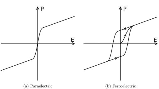
Ferroelectricity is the capability of a material to exhibit spontaneous electric polarization that requires external influence, such as an applied electric field, to be reversed. This is different from paraelectric (or even dielectric) materials, where there is no polarization without external field being applied. This can
be seen in a plot of energy vs. polarization (fig. 2.2 on the facing page) for
the two types of materials. In a ferroelectric material, the energy minima are
found at non-zero levels of polarization.19,20
The effect this has on the polarization of the material is profound, and is the hallmark of ferroelectricity. A ferroelectric material, once initially polarized,
exhibits hysteresis with respect to its P-E curve (see fig. 2.3b). Thus a
fer-roelectric material essentially remembers the sign of its last polarization, and retains that even when no polarizing field is present. In comparison, a
para-electric material (fig.2.3a) would exhibit no polarization without a polarizing
2.2: Ferroelectricity 7
The order parameter, a property used to describe its phase symmetry associated
with the arrangement of atoms, is the polarization of the material. Ferroelectric
polarization results from a displacement of the center atom of the structure creating
a dipole. In BTO, this displacement occurs along the c-direction. When all the dipoles
of a material are aligned, it will maintain a non-zero electric field. The direction the
center atom moves is dependent on the applied electric field around the material.
Both directions are equal energetically, and the overall energy plot for polarization is
shown in figure
2.2
(from [8]).
Figure
2.2
shows that in the ferroelectric state, a non-polar configuration,
corre-sponding to the peak in the middle of the graph is unstable and not energetically
favorable. This barrier can be overcome with energy provided by an external
elec-tric field. Doing so will cause the center ion to gradually move from one location to
another, called switching, accounting for its characterization as a second order
tran-sition. As temperature increases, the peak will continuously decrease until the Curie
temperature is reached. This is the temperature where the transition from a
ferro-electric to paraferro-electric material occurs and is also second order. In the paraferro-electric
state, it is no longer energetically favorable to create polarization states. The graph
will simply be a parabola with the minimum at zero-displacement.
Figure 2.2: Energy and polarization profiles for a FE material below T
C(left) and
above T
C(right).
(a) Paraelectric
The order parameter, a property used to describe its phase symmetry associated
with the arrangement of atoms, is the polarization of the material. Ferroelectric
polarization results from a displacement of the center atom of the structure creating
a dipole. In BTO, this displacement occurs along the c-direction. When all the dipoles
of a material are aligned, it will maintain a non-zero electric field. The direction the
center atom moves is dependent on the applied electric field around the material.
Both directions are equal energetically, and the overall energy plot for polarization is
shown in figure
2.2
(from [8]).
Figure
2.2
shows that in the ferroelectric state, a non-polar configuration,
corre-sponding to the peak in the middle of the graph is unstable and not energetically
favorable. This barrier can be overcome with energy provided by an external
elec-tric field. Doing so will cause the center ion to gradually move from one location to
another, called switching, accounting for its characterization as a second order
tran-sition. As temperature increases, the peak will continuously decrease until the Curie
temperature is reached. This is the temperature where the transition from a
ferro-electric to paraferro-electric material occurs and is also second order. In the paraferro-electric
state, it is no longer energetically favorable to create polarization states. The graph
will simply be a parabola with the minimum at zero-displacement.
Figure 2.2: Energy and polarization profiles for a FE material below T
C(left) and
above T
C(right).
(b) Ferroelectric
Figure 2.2: Example plots of the energy required to polarize a material. Ferroelectric materials (b) have non-zero polarization at the energy minima. Above TC all ferroelectric materials
transition to a paraelectic phase (a). As temperature increases, the energy minima will approach one another.
(a) Paraelectric (b) Ferroelectric
Figure 2.3: Example plots of the polarization as a function of applied field. (a) Paraelectric materials have two regions of polarizability; at low E the polarization increases quickly with the
field, as E increases the rate of increase decreases. (b) Ferroelectric materials show similar behavior, but additionally have hysteresis. This means that the films are switchable between
Chapter 3
Synthesis Methods
Synthesis of perovskite oxides has been demonstrated using a wide range of techniques. These range from solution-based processing methods (sol-gel approach), to physical vapor methods (molecular beam epitaxy and pulsed laser deposition), and gas phase chemical methods (chemical vapor deposition and atomic layer deposition). This review will briefly discuss sol-gel and CVD methodology, but will focus in more depth on films deposited via ALD.
3.1
Sol-Gel Processing
Sol-gel processing is a very commonly used technique for producing oxide films of a wide variety of types. It is rather straightforward in its method, but it is nonetheless a very powerful method for producing films with complex stoichiometries. Being a wet-chemical deposition technique, sol-gel has both advantages and disadvantages. It is a fairly low temperature deposition tech-nique, but in order to obtain a fully dense and crystalline film a sintering and annealing step is often required. The solution-based nature of the chemistry lends itself to very close control of tolerances in the composition of the final film.23,24
Sol-gel processing starts with the production of a colloidal solution contain-ing all of the elemental precursors that are desired, in the precise ratios desired in the final film. Generally these precursors are metallic salts or metallic alkox-ides, which are combined and then treated to undergo various co-reactions (hydrolysis, polycondensation, etc.) to form colloidal particles which become suspended in the solvent. By adjusting the pH and viscosity, the precursor sol can be converted into a gel which can be used to form a wide variety of
structures such as fibers or powders.25,26
For film synthesis, generally the sol is kept in a relatively low viscosity state and applied to a substrate via spin-coating techniques. Modulating the sol vis-cosity, rotor speed, and spinning time allows for relatively fine control over film thickness on planar structures, from the nanometer-scale to the micron-scale. The spun fluid is then heated to liberate any remaining solvent and catalyze
10 Chapter 3: Synthesis Methods
the formation of the fully gelled structure. This low-density structure can sub-sequently be heat treated at a much higher temperature to sinter and anneal the film, providing a much denser sample as well as control over crystallinity and phase. This improves the mechanical stability of the film, due to the den-sification, and can improve material properties by controlling phase purity by
the anneal step.23–26
Sol-gel films are very commonly used to produce many different types of
high-tech oxide films. PbZrxTi1-xO327 is a very common ferroelectric material
that is commonly produced in powder, film, and bulk forms via this technique. BaSrxTi1-xO3 is another.28
Some of the disadvantages of sol-gel film deposition is the lack of truly pre-cise control over the film thickness, its difficulty in evenly coating many types of 3-dimensional structures, as well as being somewhat difficult to integrate
into conventional lithographic electronics processing.23–26
3.2
Metallorganic Chemical Vapor Deposition
Metallorganic chemical vapor deposition (MOCVD) is a commonly used technique for depositing many different types of thin film materials. It is especially common for MOCVD to be used to deposit semiconductor films (a-Si, Ge, III-V, II-VI, etc.); these films can also be doped to varying degrees with high precision.6,7,29
A CVD process begins with the introduction of reactant vapors into the reactant chamber. The chamber is heated to a temperature sufficient to cause pyrolysis — thermal cracking — of the reactant. This liberates the desirable element, the metallic portion of the compound, allowing it to adsorb to the substrate. Over time a thin film is deposited. Films of multiple elements are formed by introducing two different reactants into the chamber simultaneously;
the same principle works for dopants, but at a much lower concentration.6,7,29
One advantage of CVD, partly due to the high deposition temperatures involved, is the ability to have the film deposit epitaxially to the substrate. This allows for the creation of perfect, or nearly perfect depending on the lattice matching between film and substrate, interfaces. This is very desirable
3.3: Atomic Layer Deposition 11
3.3
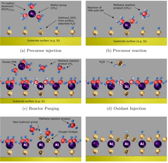
Atomic Layer Deposition
Atomic Layer Deposition (ALD) is a modification on standard CVD pro-cesses, with a few major differences. The defining aspect of an ALD process is the separation of the overall reaction into two steps: first the precursor is
allowed to react with the substrate surface (see reaction R 3.1), excess
reac-tant is purged from the chamber and an oxidizer is introduced to complete
the reaction (see reaction R 3.2).8 These reactions show a very simple ALD
reaction between trimethylaluminum (TMA, Al(CH3)3) and water.
Al(CH3)3+ M−OHsurf −→ M−O−Al(CH3)2 surf + CH4 (R 3.1)
M−O−Al(CH3)2 surf + 2 H2O −→ M−O−Al(OH)2 surf + 2 CH4 (R 3.2)
In this example, it is seen that the first stage allows the TMA to react with
the hydrated substrate surface to form part of a layer of alumina (Al2O3),
lib-erating a molecule of methane as a byproduct. In the next step, the remaining ligands are stripped away from the bound TMA molecule and replacing them with hydroxyl groups. This returns the system to the initial state — where the surface is presenting sites available to react with more TMA — and the cycle
is completed. A graphical example of this process can be found in figure 3.1.
Having only surface reactions be permitted, as opposed to CVD where gas-phase interactions dominate, affords ALD a number of unique characteristics.
One of these is the concept of the “self-limiting” growth mode.8 This behavior
arises from the limited number of available reaction sites; when all of these have either been reacted with or made unavailable by a blocking mechanism such as stearic hindrance from other local chemisorbed precursor the reaction can no longer proceed. At this point, additional available precursor is not going to be utilized, and instead will be removed and treated as waste material. The system is then evacuated, and a inert purge gas such as dry nitrogen or argon is flowed through the reactor. The purge gas serves both to push any remaining gases out of the reactor as well as to help desorb physisorbed species from the surface. The system would then again be evacuated, and the oxidant introduced and then pumped away to complete the cycle. Because of the self-limiting behavior of the reactants it is possible, in fact preferable, to utilize reactants that have highly energetic reactions with their corresponding surface site. For ALD, having fast and energetic reactions allows for rapid completion of the half-cycle, which allows for faster cycle times and thus higher
12 Chapter 3: Synthesis Methods
Section 8 Recipe Development (Advanced)
©2009 Cambridge Nanotech Inc. Confidential Rev 0.92 Draft
Savannah Maintenance Manual 70
Atomic Layer Deposition: Principle of Al2O3 formation
Atomic Layer Deposition (ALD) is a technique that allows growth of thin films, atomic layer by layer. The typical ALD reaction is illustrated via the formation of Al2O3 from trimethylaluminum or TMA, Al(CH3)3, and water,
H2O.. Recipes for other materials can be found in the literature.
Step 1: Introduction and adsorption of precursor A to the surface.
The precursor, trimethylaluminum chemically reacts with hydroxyl groups on the surface of the substrate, liberating methane. This process is called chemisorbtion. The reaction is self-limiting as the precursor does not react with adsorbed aluminum species.
Tri-methyl aluminum Al(CH3)3(g) C H H H H Al O Hydroxyl (OH) from surface adsorbed H2O Methyl group (CH3)
Substrate surface (e.g. Si)
Reaction of TMA with OH C H H H H Al O Methane reaction product (CH4)
Substrate surface (e.g. Si)
H C H
H H C
(a) Precursor injection
Section 8 Recipe Development (Advanced)
©2009 Cambridge Nanotech Inc. Confidential Rev 0.92 Draft
Savannah Maintenance Manual 70
Atomic Layer Deposition: Principle of Al2O3 formation
Atomic Layer Deposition (ALD) is a technique that allows growth of thin films, atomic layer by layer. The typical ALD reaction is illustrated via the formation of Al2O3 from trimethylaluminum or TMA, Al(CH3)3, and water,
H2O.. Recipes for other materials can be found in the literature.
Step 1: Introduction and adsorption of precursor A to the surface.
The precursor, trimethylaluminum chemically reacts with hydroxyl groups on the surface of the substrate, liberating methane. This process is called chemisorbtion. The reaction is self-limiting as the precursor does not react with adsorbed aluminum species.
Tri-methyl aluminum Al(CH3)3(g) C H H H H Al O Hydroxyl (OH) from surface adsorbed H2O Methyl group (CH3)
Substrate surface (e.g. Si)
Reaction of TMA with OH C H H H H Al O Methane reaction product (CH4)
Substrate surface (e.g. Si)
H C H H H C (b) Precursor reaction
Section 8 Recipe Development (Advanced)
©2009 Cambridge Nanotech Inc. Confidential Rev 0.92 Draft
Savannah Maintenance Manual 71
Step 2: Removal of the unreacted precursor and reaction products.
Unreacted precursor, either in the gas phase or physically adsorbed (but not chemically bonded to the surface) and the methane (CH4) liberated from the reaction are removed by evacuation of the sample chamber.
Removal is added by flowing inert gas over the surface.
Step 3: Introduction and adsorption of precursor B to the surface.
Water reacts with the methyl groups on the deposited aluminum atoms forming both Al-O-Al bridges, as well as new hydroxyl groups. The formation of hydroxyl groups readies the surface for the acceptance of the next layer of aluminum atoms. Methane is liberated as a by-product
C H H Al O
Excess TMA Methane reaction
product CH4
H HC
Substrate surface (e.g. Si)
C H H Al O H2O H HC O H H (c) Reactor Purging
Section 8 Recipe Development (Advanced)
©2009 Cambridge Nanotech Inc. Confidential Rev 0.92 Draft
Savannah Maintenance Manual 71
Step 2: Removal of the unreacted precursor and reaction products.
Unreacted precursor, either in the gas phase or physically adsorbed (but not chemically bonded to the surface) and the methane (CH4) liberated from the reaction are removed by evacuation of the sample chamber.
Removal is added by flowing inert gas over the surface.
Step 3: Introduction and adsorption of precursor B to the surface.
Water reacts with the methyl groups on the deposited aluminum atoms forming both Al-O-Al bridges, as well as new hydroxyl groups. The formation of hydroxyl groups readies the surface for the acceptance of the next layer of aluminum atoms. Methane is liberated as a by-product
C H H Al O
Excess TMA Methane reaction
product CH4
H HC
Substrate surface (e.g. Si)
C H H Al O H2O H HC O H H (d) Oxidant Injection
Section 8 Recipe Development (Advanced)
©2009 Cambridge Nanotech Inc. Confidential Rev 0.92 Draft
Savannah Maintenance Manual 72
Step 4: Removal of the unreacted precursor and reaction products via evacuation and/or inert gas flow.
Step 5: Repeat to create layers
The process begins again with the introduction of precursor A followed by B. Atomic layers are built up one after the other.
New hydroxyl group
Oxygen bridges Methane reaction product
H Al O O O Al Al H Al O O O O Al Al
(e) Oxidation Reaction (Ligand Exchange)
Section 8 Recipe Development (Advanced)
©2009 Cambridge Nanotech Inc. Confidential Rev 0.92 Draft
Savannah Maintenance Manual 72
Step 4: Removal of the unreacted precursor and reaction products via evacuation and/or inert gas flow.
Step 5: Repeat to create layers
The process begins again with the introduction of precursor A followed by B. Atomic layers are built up one after the other.
New hydroxyl group
Oxygen bridges Methane reaction product
H Al O O O Al Al H Al O O O O Al Al
(f) Completed Cycle, Regenerated Surface
Figure 3.1: Example schematic of the process of an ALD deposition cycle. This example illustrates the reaction of TMA and water to form alumina (Al2O3).
3.3: Atomic Layer Deposition 13
throughputs. In CVD such energetic reactions are very difficult to control, and instead precursors that have only mild reactions — with a Gibbs free energy exchange as close to zero as possible while remaining negative — with each other are preferred. These require more effort to develop and require that the process be carefully controlled, as the reactions often can either easily
extinguish themselves or rapidly accelerate in different conditions.8
In the implementation of most ALD systems, the purge gas is also used as a carrier gas for the precursors. Thus a constant flow of gas is passed through the system, instead of having it occasionally fully evacuated, and the precursor is able to be delivered from its source to the reactor more effectively. For some precursor compounds, in particular those with a low vapor pressure, having carrier-assisted transportation can greatly improve the behavior of the
system.8
Because of the self-limiting behavior, each deposition cycle is limited to a theoretical maximum of one monolayer of material (in practice a much lower
coverage per cycle is attained), which is far less than a unit cell.8 Generally
per cycle growth rates range between 0.03–1.5 ˚A, with the rate being nearly
invariable during most of the deposition. This gives the second defining
charac-teristic of ALD: very high (˚A level) thickness resolution. The downside of this
aspect is that growths are generally much slower than other types of deposi-tions; ALD is generally slower by an order of magnitude or more than a similar CVD process, as an example. This has proved invaluable in many processes where high precision is critical, such as electronics manufacturing. Intel, for example, uses ALD to deposit extremely precise layer thicknesses of a high-κ
dielectric (such as hafnia, HfO2) for use as the gate oxide in transistors.1,30
There are a wide range of binary oxides for which ALD processes have been
developed. A deposition for alumina (Al2O3, one of the first ALD materials
developed, was discussed briefly above and the method is is common use.11,31
High-k gate oxides such as hafnia and zirconia (ZrO2), along with some of their
nitrides and silicides, are under intense research to develop industrial processes
for their use in integrated circuitry.1,30 Other transition metal oxides, such as
titania (TiO2) and iron oxide (Fe2O3), have also had ALD deposition processes
developed for their deposition.3,32
The methods described above will produce a layer of a binary oxide material
(AOx); if more complex materials are desired the method must be changed.
The basic principles remain the same; one would perform the procedure for depositing a cycle of a binary oxide and then change the precursor and deposit
14 Chapter 3: Synthesis Methods
another cycle of a different oxide material. For example, if one wished to
deposit PbTiO3, one would begin by depositing a layer of TiO2 and then
depositing a layer of lead oxide (PbO). Repeating this set of cycles — a
super-cycle — would eventually form the PbTiO3 film.
However, deposition of complex oxides is not this simple in practice. In many cases, running each oxide cycle in a 1:1 ratio will deposit a non-stoichiometric material. This makes it necessary to modify the method to deposit more of one type of oxide than the other. For example, if a material is Ti-rich the super-cycle ratio would be modified to increase the number of lead oxide super-cycles as compared to the titania cycles. Careful tuning of the deposition conditions, which include a variety of different factors, is required to obtain a desired and consistent film stoichiometry.
In addition to lead titanate, there are other ternary oxide systems that are
being investigated. Examples of which are bismuth ferrite (BiFeO3) or barium
strontium titanate (BaSrxTi1-xO3).33
ALD reactions are rather sensitive to a number of factors, such as tempera-ture. The temperature must be high enough that the reactants have sufficient energy to drive the surface reaction but not so high as to allow undesirable reactions to activate (e.g. precursor cracking or surface material desorption). Precursor selection is also very important, for similar reasons. The precursors must also be incapable of reacting with themselves, to allow the self-limiting
Chapter 4
Thin Film Growth
4.1
Precursor Selection
4.1.1 Titanium Source
The source of titanium that was used was titanium(IV) isopropoxide
(Ti-o-i-Pr, Ti(OCH(CH3)2)4). This compound is very commonly used in ALD
literature.34–39 It is a liquid precursor with a high vapor pressure and reacts
easily with most oxidizers; the most commonly used oxidant for this reaction
is water vapor, similar to the TMA-H2O reaction (see section3.3 on page 11).
4.1.2 Lead Source
One of the primary tasks of this project was to identify viable ALD precur-sors for the deposition of lead into the thin films. Potential candidates needed to meet a few stipulations. First, it needed to have chemical and thermal properties compatible with the ALD reactor. It was also desired that previous studies had used it in other ALD processes. Finally, it was important that the compound was available in quantity from chemical suppliers.
To this end, there were four potential candidates that were investigated
which were identified from previous literature reports: tetraphenyllead (Ph4Pb),4
lead(II) bis(2,2,6,6-tetramethyl-3,5-heptanedionato) (Pb(TMHD)2),14 lead(II)
hexafluoroacetylacetonate (Pb(HFAc)2),40and lead
bis(3-N,N-dimethyl-2-methyl-2- propanoxide) (Pb(DMAMP)2).41
Ph4Pb was one of the commonly used compounds in both ALD and MOCVD
references, but it was found to have insufficient volatility for use in the ALD (up
to its maximum evaporation temperature of 200◦C)4 and was thus discarded
as a candidate. Pb(TMHD)2 was another commonly referenced precursor,14as
was Pb(HFAc)2.40 Pb(DMAMP)2 was seemingly a viable choice, with a very
high vapor pressure at low temperatures,41 but it was not readily available
from chemical suppliers and was very costly to purchase which also kept it from being considered further.
16 Chapter 4: Thin Film Growth
Thus, the two compounds Pb(HFAc)2 and Pb(TMHD)2 were investigated
in detail as potential candidates for the lead precursor in the ALD deposition
of PbTiO3. Samples of both precursors were obtained from Strem Chemicals,
inc.42 and were analyzed to determine which would be most viable. Tests
included thermogravimetric analysis (TGA), differential scanning calorimetry (DSC), as well as test depositions of ALD films.
4.1.3 Oxidizer
Three potential oxidants were considered; these included water, oxygen, and an ozone/oxygen mix. The choice of oxidant depends heavily on the reactivity with the potential precursors.
The choice of titanium(IV) isopropoxide as the titanium source allows for any of the three selected oxidizers to be used. A hydrolysis reaction will occur when exposed to water vapor; in the case of oxygen or ozone the ligands will
be consumed via a combustion reaction.8,32,43
Based on literature reports, the two lead precursors under investigation do not undergo hydrolysis when exposed to water, and as such require the use of the combustion pathway. In addition, through the deposition of test films,
it was found that the reaction proceeded more completely when the O3/O2
mixture was used. For simplicity of the process, the O3/O2 mix was used for
both half-reactions.44
4.2
Substrate Preparation
Fabrication and preparation of substrates was an important part of the deposition process. Some substrates were purchased and simply cleaned, others needed to be fabricated or otherwise processed prior to cleaning and use in deposition. Three main types of substrates were used: thermally oxidized single-crystalline silicon (100) wafers, silicon wafers that had a thin layer of platinum deposited on the surface, and strontium titanate (100) single crystal substrates.
4.2.1 Si(100)
The silicon substrates were prepared in a simple manner. 4 in. diameter silicon wafers with 200 nm of thermally grown oxide were diced into 1.5 cm x 1.5 cm pieces. When a sample was to be used for deposition, it was cleaned by
4.2: Substrate Preparation 17
one minute of sonication in acetone, followed by isopropanol, with a subsequent 5 minutes of sonication in deionized (DI) water. These were then air dried with dry nitrogen. Finally, the substrates were cleaned in a oxygen plasma cleaning
system to remove any remaining organic residues present on the surface.45
4.2.2 Platinized Si(100)
Platinized silicon substrates were prepared in a similar manner to the
Si(100) samples. For the initial platinization, a large piece (5 x 5 cm2) of
pre-cleaned silicon wafer with a thin layer of native oxide, as opposed to the 200
nm of thermally grown oxide, was prepared in the manner described above.45
Then a 15 nm layer of platinum was deposited via ALD.46The substrates were
then cleaved into smaller pieces for subsequent use.
If the samples are stored, it is recommended to again clean the samples in
the standard procedure prior to use (see 4.2.1 on the facing page).
4.2.3 Single Crystal STO(100)
Oxide crystal substrates were prepared in such a fashion as to promote the formation of atomically flat terraces. This has the advantage of promoting a uniform surface species across the entire sample — the etchant used in this
process leaves the sample titania-terminated.47
To prepare these samples, the substrates are first pre-cleaned in a four step sonication process. The samples were cleaned for five minutes in each of acetone, methanol, and isopropyl alcohol. Subsequently, the samples were
sonicated for fifteen minutes in DI water.47 The substrates were then immersed
into a commercially prepared buffered hydrofluoric acid (BHF) solution to etch for 30 seconds, then removed and flushed with copious quantities of DI water to purge any remaining BHF solution. Once the sample is thoroughly rinsed,
the samples are dried using dry nitrogen.47
After the etching process, the samples are annealed at 950◦C for one hour.47
Once the samples are cooled, they are ready for immediate use. AFM can be used to confirm the presence of well-defined atomic terraces.
If the samples are stored, it is recommended to again clean the samples in
18 Chapter 4: Thin Film Growth
4.3
Deposition Parameters
There are four main parameters that can affect the behavior of an ALD deposition. These are the growth temperature, the dosage of each precursor, the purge time between doses, and any extended precursor-surface exposure time.
4.3.1 Growth Temperature
The temperature of the growth chamber has a strong effect on reaction behavior. ALD reactions are sensitive to temperature, and will only proceed properly within a certain range known as the ‘ALD window.’ Outside of this range, the reaction enters one of a number of different regimes; these are determined by comparing the growth rate of the deposition to that of a reaction
in the self-limiting saturated “ALD mode.”8,32,43,48
If the growth temperature is less than the lower bound of the ALD win-dow, the two regimes are condensation limited and activation energy limited. Condensation limited growth occurs when the substrate temperature is low enough that precursor condenses onto the surface without reacting with the presented sites. This causes higher than expected growth rates, and a lack of self-limiting behavior. If the reaction instead proceeds into the activation energy limited regime, molecules of precursor lack sufficient energy to react
with the surface. This is characterized by lower deposition rates.8,43
Conversely, if the reactor temperature is excessive the reaction again be-come anomalous. Decomposition limited growth, characterized by excessive deposition, is a result of thermal cracking of the precursor materials. This re-action is not limited to the surface, and accounts for the extra material being deposited. Lower deposition rates indicate that the temperature is sufficient
to cause desorption of previously-reacted material from the sample.8,48
For an ALD run to be successful, the acceptable temperature window for all of the reactions should overlap in some temperature range. This can become
difficult with reactions requiring multiple metal precursors (e.g. PbTiO3, a
combination of TiO2 and PbO), as these can have widely varying ALD windows
4.3: Deposition Parameters 19
4.3.2 Precursor Dosage
The dosage of precursor or oxidant to the surface is another parameter of critical importance. An ALD reaction requires a minimal amount of precursor to sufficiently saturate the surface, while it is beneficial to minimize any excess precursor as it will be a wasted byproduct (minimizing costs, environmental impact, etc.).
The vaporization behavior of the precursor can have a dramatic impact on how simple or difficult it is to deliver a saturating dose to the surface. Some materials have readily available precursors with high vapor pressures; titanium isopropoxide and trimethylaluminum (TMA) are both liquids, and
tetrakis(dimethylamido)hafnium (Hf{N(CH3)2}4) is a low-melting
tempera-ture solid. These are commonly used precursors for depositing their respec-tive oxides. This vapor pressure becomes an important consideration when
choosing a potential compound for use in ALD (as discussed in section4.1 on
page 15).8,32,43,48,49
Insufficient dosing is apparent in a deposition run by a slower than average growth rate, or also as a non-uniform deposition rate across the sample. How-ever, overdosing is not readily apparent in an ALD-mode deposition. The dose must be lowered to a point where the dose is insufficient, and then increased back to a saturating level.
Controlling the dose is dependent on injection time (which is the time the valve between the process line and the precursor storage vessel is open), precur-sor temperature, and the cycle duration (time between precurprecur-sor injections). By increasing either the injection time or the precursor’s temperature the dose is increased, except in some cases with low vapor pressure materials. In this case, it can sometimes be found that the evaporation kinetics are slow and it takes additional time to build up a sufficient amount of vapor to provide a dose to the reactor.8,32,48
If necessary, multiple doses of precursor can be delivered to the sample during each cycle to increase the total delivered dose.
4.3.3 Purge Time
Purge time is important as it gives time for the N2flow to flush any
remain-ing byproducts, excess reactants, and physisorbed (as opposed to chemisorbed) species from the substrate surface and out of the reactor zone. It also allows time between cycles which allows for low vapor pressure precursors to
regen-20 Chapter 4: Thin Film Growth
erate evaporated material; if this time is too short to fully regenerate the dose in the cylinder the precursor will eventually appear to be depleted during the
course of the deposition.8,43
4.3.4 Exposure Time
Exposure time denotes the time where the precursor is held in the reaction zone to increase the amount of time during which the surface reaction can oc-cur. This is beneficial for two types of depositions. In the case of low-reactivity precursors, it increases the amount of time that the precursor is available to the surface, greatly increasing the surface coverage per cycle. Exposure mode is also beneficial for depositing upon three dimensional structures, especially those with a high aspect ratio, e.g. nanotube templates. This extra dwell time of the precursor allows for diffusion of reactant into the structure, for a uni-form coverage upon the entirety of the surface. Purge time must be increased
accordingly to allow for byproducts to diffuse back out of the structure.8,43,50
4.4
Post-Deposition Annealing
Two types of annealing procedures were used in this study. Oven annealing, with the simple use of a furnace in ambient atmosphere; and rapid thermal annealing (RTA), characterized by very high heating and cooling rates and
performed in an inert atmosphere (dry N2).
4.4.1 Oven Annealing
In oven annealing, the samples to be processed are placed in a cold oven in the ambient atmosphere of the laboratory. The samples are then heated
grad-ually at a rate of 10–25◦C per minute up to the final annealing temperature,
which ranged from 600–900◦C. The samples are then allowed to heat-treat for
120 minutes at the process temperature, and then the furnace is allowed to return to room temperature.
This conventional heating pattern allows the sample to obtain its equilib-rium crystalline phase composition, be that a single crystalline phase, poly-crystalline, or involve multiple phases or materials. This was the annealing method most commonly used during this study.
4.4: Post-Deposition Annealing 21
4.4.2 Rapid Thermal Annealing
Rapid thermal annealing (RTA), as its name suggests, involves very high
heating and cooling rates. RTA systems can heat at rates over 10◦C per
second, allowing the chamber and sample to reach the process temperature very quickly. Similarly, processing times are generally much shorter, and are generally no longer than 10–15 minutes. Cooling, facilitated by a water cooling apparatus, also occurs rapidly. These sharp gradients can have different effects on the crystal structure of the film, locking in different phases in the material that may otherwise dissociate given more time during heating or cooling.
In this study samples processed via RTA used a HeatPulse™ RTA system,
which allowed for automatic control of the process. Sample processing
Chapter 5
Material Characterization
5.1
Thermal Analysis
5.1.1 Thermogravimetric Analysis
Thermogravimetric analysis (TGA) is a very useful tool when attempting to determine the viability of a precursor in an ALD process. It allows for estimation of vaporization rate at various temperature rates as well as indi-cations of chemical breakdown (i.e. thermalization) which would hinder the precursor’s usefulness.
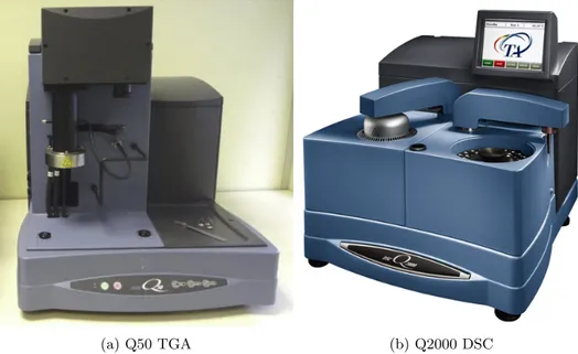
At its core, TGA is a measurement of mass loss as a function of temperature or time. A small sample (1–10 mg) of material is placed in a microgram balance pan and suspended inside a furnace. The furnace is then heated at a specified rate while the sample mass is carefully monitored. For the experiments used in this study (evaluation of thermal vaporization and thermal degradation) it is important to ensure that the testing environment is inert. This is accomplished by using a platinum pan in the microgram balance and constantly purging the furnace with a small flow of dry nitrogen gas. The heating rate can be varied according to a pre-determined program to provide more information at various
individual temperatures.51–54
This technique was used to evaluate various precursor candidates for the
lead oxide half of the PbTiO3 deposition procedure. The instrument used was
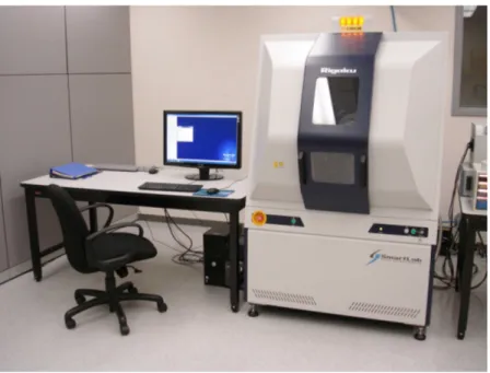
a Q50 TGA device (fig. 5.1a on the following page). A detailed discussion of
TGA procedures and the investigated chemicals can be found in subsequent
chapters (see 4.1 on page 15 and 7.1 on page 43).
5.1.2 Differential Scanning Calorimetry
Differential scanning calorimetry (DSC) is a technique that allows for the determination of various critical temperatures for a material, and also can highlight changes in chemical structure due to degradation or other thermal processes.
24 Chapter 5: Material Characterization
(a) Q50 TGA (b) Q2000 DSC
Figure 5.1: Photograph of the thermal analysis instrumentation used during this study, made by T.A. Instruments, inc.
DSC is the analysis of energy absorption as a function of temperature, which is the essence of calorimetry. DSC uses a sample and reference system to isolate the energy absorbed by the sample from that of the holder pan. Sample sizes usually range from 0.1–2 mg of material; as the samples used in this study are volatile the sample pans are hermetically sealed to prevent mass loss. The sample and reference pans are then placed inside a thermally insulated chamber. The temperature of each is carefully monitored, and differ-ing amounts of heat are applied to negate the temperature difference between the sample and reference. The difference in absorbed heat as a function of temperature is then given as the result. In general, experiments include both heating and cooling curves to gain a complete understanding of the different energies.54–56
DSC was used to analyze the behavior of precursor chemicals around their evaporation and reaction temperatures. The main goal was to determine if the material underwent any thermally-activated degradation processes at either of these two temperature ranges. At the evaporation temperature, the sample was generally cycled multiple times to simulate actual use in the ALD. These
measurements were taken using a Q2000 DSC system (fig.5.1b) made by T.A.
5.2: Thin Film Characterization 25
Figure 5.2: Schematic of the beam path during an ellipsometric measurement, critical parameters are indicated
5.2
Thin Film Characterization
5.2.1 Variable Angle Spectroscopic Ellipsometry
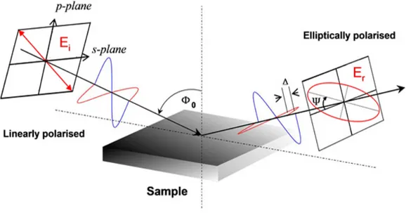
Ellipsometry is a powerful non-destructive optical technique that allows for the determination of a large number of properties of complex thin film structures. The basic tenet of ellipsometry relies on the analysis of the change in polarization state of a reflected light beam after interaction with the sample. The incident beam is generally linearly polarized, but upon reflection becomes elliptically polarized due to a phase shift in the components of the beam in the s- and p-plane, as well as a change in their relative amplitudes. The phase shift is correlated to the ellipsometric parameter ∆, while the amplitude change is given by tan Ψ (Ψ is the angle between the s-plane and the major axis of the ellipse). The last major parameter is the incident angle, denoted by Φ. A
schematic diagram illustrating these parameters can be seen in figure5.2.57–59
From these parameters, one can directly determine the ratio between the
reflectance in the p-plane (rp) and the reflectance in the s-plane (rs) from
the fundamental ellipsometric relation (eqn. 5.1 on the next page). Once this
relationship is known, the Fresnel equations (eqn.5.2 on the following page) can
be used to numerically determine the value of the complex index of refraction at the specific wavelength of the incoming beam. The complex index of refraction