“Applied Electromagnetism in Electrical and Biomedical
Engineering, Electronics, Smart Sensors, Nano-Technologies”
PhD Thesis
Intrinsic variability of nanoscale
CMOS technology for logic and
memory
ING/INF-01
Advisor:
Prof. Giuseppe IANNACCONE
_____________________________
Author:
1
Contents ... 1
Acknowledgements ... 3
Introduction ... 5
1 Variability in CMOS technology ... 7
1.1 Main factors of variability of the CMOS technology ... 15
1.1.1 Random discrete dopant (RDD) ... 18
1.1.2 Line edge roughness (LER) and line width roughness (LWR) . 21 1.1.3 Oxide thickness variation (OTV) or Surface Roughness (SR) .. 23
1.2 Mismatch ... 24
1.3 Delays of multi-level logic ... 29
1.4 Noise margins of SRAM ... 33
2 State of the art... 39
2.1 Random discrete dopant (RDD) ... 39
2.2 Line edge roughness (LER) ... 48
2.3 Oxide thickness variation (OTV) or Surface Roughness (SR) ... 57
2.4 Combined effects ... 60
3 Analysis of the threshold voltage dispersion in different MOSFET structures ... 75
3.1 Methodology ... 78
2
3.3 Effect of random dopant distribution ... 90
3.4 Conclusion ... 100
3.5 Appendix: Analytical model for the dependence of threshold voltage on gate length. ... 102
4 Variability in Flash memory cells ... 107
4.1 Flash memory ... 107 4.2 Variability ... 117 4.3 State of art ... 119 4.4 Our method ... 120 4.5 32 nm Flash Cell ... 121 4.5.1 Device geometry ... 121 4.5.2 Doping profile... 124
4.6 Threshold voltage variability ... 125
4.6.1 Random Discrete Dopants ... 127
4.6.2 Line Edge Roughness ... 130
4.6.3 Line Width Roughness ... 131
4.6.4 Oxide Thickness Fluctuations ... 133
4.6.5 Interface-Trapped Charge (ITC) ... 134
4.7 Conclusions ... 139
3
First of all, I would like to thank my tutor Prof. Giuseppe Iannaccone for the valuable guidance during the course of this work.
I also would like to thank the Ing. Alessandro Nannipieri for his support and for the stimulating discussions about Sentaurus TCAD.
I also wish to express my gratitude for my mother, my father, Deborah and Andrea, for the support they have always given me.
A special thanks for my boyfriend who is a person very important in my life. Finally I thank my dearest friends who are always close to me.
5
The continuous downscaling of CMOS technology, the main engine of development of the semiconductor Industry, is limited by factors that become important for nanoscale device size, which undermine proper device operation completely offset gains from scaling.
One of the main problems is device variability: nominally identical devices are different at the microscopic level due to fabrication tolerance and the intrinsic granularity of matter. For this reason, structures, devices and materials for the next technology nodes will be chosen for their robustness to process variability, in agreement with the ITRS (International Technology Roadmap for Semiconductors). Examining the dispersion of various physical and geometrical parameters and the effect these have on device performance becomes necessary.
In this thesis, I focus on the study of the dispersion of the threshold voltage due to intrinsic variability in nanoscale CMOS technology for logic and for memory. In order to describe this, it is convenient to have an analytical model that allows, with the assistance of a small number of simulations, to calculate the standard deviation of the threshold voltage due to the various contributions.
In the first chapter of the thesis will address the problem of variability of physical and geometrical parameters in CMOS technology and will analyze the
6
main factors of variability and the effect of variability on the performance of electronic circuits.
The second chapter will proposed an overview of the state of the art of research in variability, taking into account various mechanisms and their combined effects.
In the third chapter we will describe our model to investigate the dispersion of the threshold voltage based on sensitivity analysis. We have considered various structures, for which results from three-dimensional atomistic statistical simulations were available, in order to compare and verify the validity of our method: in particular a 32 nm ultra-thin body SOI MOSFET and a 22 nm double-gate MOSFET adopted within the EC PULLNANO Project, one bulk 45 nm NMOSFET within the ENIAC project MODERN and a 32/28 nm CMOS process developed by STM again for the MODERN project.
In the fourth chapter we consider the variability of Flash memory devices, focusing on a template of a flash memory cell obtained in collaboration with Micron for the 32 nm technology node. We shall see the specificity of studying device variability in the context of nonvolatile memories
7
The semiconductor industry was born with the invention of the first bipolar transistor in 1948. In 1961 appeared the first planar circuit and in 1964 it was the turn of the first MOSFET. Today the progress of the semiconductor industry has led to microprocessors operating at GHz frequencies, to microprocessors with more than 1 billion transistors and GByte memory chips.
This rapid technological progress had been predicted in 1965 in a famous speech by Gordon Moore. Moore said that the number of transistors per square inch present on a chip would double every 18 months, achieved both by reducing the size of the transistor, and by increasing the size of the single circuit. This prediction became the so-called "Moore's Law" (Fig. 1.1).
The further reduction in the size of MOS transistors, however, requires the introduction of new materials and new architectures that take the place of conventional planar MOS.
8
Fig. 1.1 The time progresses of Moore's law [1].
One of the main causes of the rapid improvements of integrated circuits have to be found in the excellent performance and scaling properties of MOS transistors, for the first time described by Dennard in 1974: he saw that reducing the horizontal size, vertical size and operating voltage, we can obtain simultaneous improvements in the density of transistors, the switching speed and switching energy. Since then, the recipes for scaling have been updated to modern processes. However, every 2-3 years we see a reduction in the minimum size of about a factor of 0.7 and each generation provides transistors that are smaller, faster and use less energy [2].
A method to estimate the delay of gates based on MOS transistors is the use of the CV/I metric. In this metric, the switching speed can be estimated when
2X transistors every 2 years
Traditional Scaling Era
9
typically larger than the gate capacitance). However, a metric is especially useful when there is not a complete set of transistor parameters for a more rigorous comparison.
Another important characteristic of the MOS transistor is to reduce the amount of energy used during a switching event. The reduction in switching energy is due to the combination of several factors: lower parasitic capacitance, smaller feature sizes, lower supply voltage. A metric to estimate the switching energy of MOS transistor is CGATEVDD
2
, using the gate capacitance of the transistor and the supply voltage. This is also a simplified metric, which omits some factors of the second order, but it is useful to estimate the trends of the various technology generations. The transistor switching energy has become increasingly important because of constraints on the overall power consumption.
Scaling also poses performance challenges. Scaled MOS transistors require reduced threshold voltages than in turn lead to higher subthreshold leakage (IOFF). Another limitation is the gate oxide thickness reduction: the leakage
current of the gate oxide increases exponentially with each new generation due to the reduction of oxide thickness and approaches the values of the subthreshold drain current (~ 1 nA / μm).
Metal gate with high-k dielectric have been implemented in the recent technology generations in order to allow scaling of the EOT (equivalent oxide
10
thickness), consistent with the overall transistor scaling while keeping gate leakage currents within tolerable limits.
The characteristics of the MOSFET for very small dimensions present variability issues because of the challenging lithography and because of intrinsic process variations, such as the random fluctuation of dopants in the channel regions that concern the control of the threshold voltage Vth.
To approach the issue of CMOS technology scaling, we refer to chapter
Process Integration, Devices, and Structures (PIDS) of the International
Technology Roadmap for Semiconductors (ITRS) [3], which addresses the subject of aggressive scaling of MOSFETs, treating the entire process flow for the realization of integrated circuits, considering the tradeoffs of reliability associated with new options.
This aggressive scaling drives the industry toward a series of important technological innovations, including material and process changes such as high-k gate dielectric, metal gate electrode, and at longer term, new structures such as ultra-thin, multi-gate MOSFETs (as well as FinFET).
The key objectives of the ITRS include both the identification of the main technical requirements and the key challenges in order to support the scaling of CMOS technology for the Moore's Law, and the encouragement to research and development necessary to meet the key challenges.
The ITRS provides potential solutions, which are intended as a stimulus and not as limitations to the research, exploring new and different approaches.
In the Tab. 1.1 the difficult challenges identified by the ITRS 2010 for process integration are shown.
11
Tab. 1.1 Process Integration Difficult Challenges [3].
In the ITRS Emerging Research Devices chapter, information on several new technologies proposed for beyond CMOS information processing, memory, and storage technologies was evaluated and discussed. In the Table 1.2 and Table 1.3 the difficult challenges of the emerging research devices and materials are reported.
12
13
Tab. 1.3 Emerging Research Material Technologies Difficult Challenges [3].
The Front End Processes (FEP) Roadmap focuses on future process requirement and potential solutions related to scaled field effect transistors (MOSFETs), DRAM storage capacitors, and non-volatile memory (Tab. 1.4).
14
The purpose is to define comprehensive future requirements and potential solutions for the key front end wafer fabrication process technologies and the materials associated with these devices.
Tab. 1.4 Front End Processes Difficult Challenges [3].
The limits of CMOS scaling have led researchers worldwide at the introduction of new device structures, such as ultra-thin body (UTB) silicon on insulator (SOI) devices, double-gate SOI, FinFETs. These new devices help eliminate some of the short-channel effects displayed by conventional MOSFETs. However, many old questions remain, and also new problems arise. For example, in UTB SOI devices, in double-gate MOSFET and FinFET, mechanical quantum effects significantly influence the overall behavior of the device. In addition, there are still considerable fluctuations in device parameters.
A potential solution to the unacceptable variation in threshold voltage in very small MOSFET, caused by the small number of dopants in the channel, is to use ultra-thin body, fully depleted SOI MOSFETs. For these devices the
15
to the symmetrical structure and the extremely low doping, so one can not apply the models developed for bulk planar MOSFETs.
In this regard, while for the conventional bulk MOSFET, there are several models in the literature related to analytical and numerical fluctuations of the parameters, which become evident with the reduction in size, relatively little has been done to these new components.
It is useful to analyze the dispersion of parameters in these new devices, to study the effects and find solutions to allow for the scaling while respecting the constraints imposed by the Roadmap.
1.1 Main factors of variability of the CMOS technology
The rapid growth of semiconductor industry over the past 40 years has been mainly the result of a constant reduction in the size of the CMOS switching elements, which form the basis of the logic circuits in almost all modern digital systems. When the size of the CMOS switches, and field effect transistors that implement them, are reduced, the integrated circuits make with them, to improve in terms of speed, density of the total circuit and cost for function.
But there are some physical limitations to the miniaturization process [4]. The International Roadmap for Semiconductors outguess that CMOS transistors with channel lengths of 7 nm become mass-produced since 2018; devices with channel lengths of 25 nm are already in production. The size of the
16
CMOS will continue to scale over the next two decades, but when they come near to the dimensions of the silicon lattice, the precise atomic configuration of the structure will become extremely important for their macroscopic properties.
Fig. 1.2 Dopants in a small transistor: the electrostatic potential is mapped from red (1 V) to blue (0 V). The fluctuations of the potential in the channel associated with the random distribution of dopants lead to have different characteristics for each device [Fig of [4]].
Mead and Keyes recognized in 1970 [5], [6] that below a critical size, the devices cannot be described, designed, modeled, or referred as a discrete semiconductors with smooth boundaries and interfaces. At the nanoscale, the effect of the number and position of dopant atoms, introduced to alter the electrical properties of different regions of field effect transistors, (Fig. 1.2) will be larger because of the small number of dopants; at the nanoscale it will therefore be important to consider that every transistor is microscopically different. The variation in the position of dopants between devices leads to
17
oxides (one or two atomic layers), becomes comparable with the thickness of the gate dielectrics itself. Thus, each device will have a different thickness of the gate, and a profile of the roughness of the interface unique.
The use of high permittivity gate insulators (high k), to replace the existing gate oxides, permits to obtain the gate thicknesses that can reduce this source of fluctuations for one or two technology generations. However, variations on the atomic scale of the position of impurity atoms, the local variations at the interface silicon / silicon dioxide over the canal, and local variations of the thickness of silicon dioxide, introduce variations in the electrostatics of the device, in the electronic transport, and in the leakage current. The granularity of the photoresist used to model the gate, will also introduce local variations in the shape of the gate itself.
With existing technology, it is impossible to associate the detailed atomic structure of individual nanoscale CMOS transistors corresponding to the characteristics of each device. Over the past decade, researchers have been focused to gain understanding of the fluctuations of the intrinsic parameters in nanoscale CMOS transistors, and they have therefore made use of numerical simulations, using more detailed mathematical models.
Key to any discussion of the fluctuations is to understand if the effect of a variation is fundamental (can be removed only with a change in the structure or in the operation of the device) or can be reduced with improvements in technology over the years [7].
18
A large number of effects of both types of variations have been documented in the literature. Examples include: highly random effects (random dopant fluctuations, RDF [8], line-edge roughness, LER [9], [10], line width roughness, LWR [10], [11], oxide thickness fluctuations, OTF [12], poly-silicon granularity PSG [13], interface trapped charges [14], non-uniformity of the charge at the interface [15]), proximity effects in the pattern (classic and OPC / RET [16]), proximity effects associated with stress (over layers, PMOS epitaxial, STI-induced [17]), proximity effects associated with the polish (STI and ILD [18]), proximity effects associated with the annealing (RTA-generated [19]), effects related to the device (pockets planted with grains of poly [20], oxide thickness [21]), and effects related to design (hot spots, falls [22]).
Of all the causes listed, it is assumed [23] that the main sources of fluctuations are:
Random Discrete Dopant (RDD)
Line Edge Roughness (LER) and Line Width Roughness (LWR) Oxide-thickness variations (OTV)
1.1.1 Random discrete dopant (RDD)
The impact of the number and placement of dopant atoms on the characteristics of the device is crucial in determining the behavior of nanoscale semiconductor devices, because these factors cause random variations in the transistor threshold voltage (Vth ) [24] - [26].
This can result in threshold voltage mismatch between transistors on die (intra-die variations) resulting in significant delay variation of logic gates and circuits [26]. The effect of random dopant fluctuations (RDF) on Vth increases
19
in this small number of dopant atoms can result in significant variations in the Vth of the transistor. Since the Vth variation due to RDF can result in significant
variation in the delay of an electronically circuit, a careful analysis of the effects of various sources of fluctuations is very important to make further progress in VLSI technology. In particular, threshold matching, which is important for some types of circuits such as SRAM and sense amplifiers, may be limited by these fluctuations [27].
For example in Fig. 1.3 the discrete dopants randomly distributed in a cube of 80 nm3 with an average concentration of 1.48 × 1018 cm-3 are shown.
20
Fig. 1.3 (a) Discrete dopants randomly distributed in a cube of 80 nm3 with an average concentration of 1.48 × 1018 cm-3. There will be 758 dopants within the cube, but dopants vary from 0 to 14 (the average number is 6) within its 125 subcubes of 16 nm3 [(b), (c) and (d)]. These 125 subcubes are then equivalently mapped in the corresponding regions of channel of the device single-gate (s), double-gate (f), triple-gate (g), and (square shaped) surrounded gate (h) for 3D simulations of sensitivity to the number-position of the dopants [Fig 1 of [28]].
It is seen that the random nature of the dopants causes appreciable dispersion of the threshold voltage, of the small signal parameters, and of the subthreshold
21
International Roadmap for Semiconductors has predicted a transition from conventional bulk devices to devices silicon-on-insulator (SOI) and then to the multi-gate SOI devices as a high-performance. As a result, nanoscale devices with vertical channel structures, such as double and triple gate and FinFET (fin-type field effect transistor) with gate surrounded, are of great interest. However, the channel doping must be used to alter the threshold voltage in the present semiconductor manufacturing processes.
Several approaches, such as small-signal analysis [30] - [32], drift-diffusion [33] - [35], and simulation with the Monte Carlo method [36] - [38] were adopted to study the issues concerning variations and fluctuations in semiconductor devices.
1.1.2 Line edge roughness (LER) and line width roughness (LWR)
Gate patterning is known to induce a no ideal (rough) edge herewith referred to as line-edge roughness (LER).
Current state of the art processes is able to consistently reproduce poly line widths below 100 nm. As the line width is scaled down, however, the roughness on the edge of the line does not scale. The total value of the LER is defined to be traditionally 3Δ, where Δ is the rms amplitude of LER that can be obtained statistically from inspection of the lines generated by a given lithography process [10]. The data collected by different processes, summarized in Fig. 1.4,
22
show that, at present, there is a minimum limit of the edge roughness of poly lines is typically on the order of 5 – 6 nm, but can have values much larger than that, depending on how the poly line was formed.
This value is larger than the requirements of the Roadmap for the devices below 100 nm, and it is alarming because the dimensional requirements are often more difficult to meet than the other specifications, for a given process.
The SIA national technology roadmap tells us that devices built as this scale are required to control gate length within approximately 8 nm [12].
A typical image of photoresist lines and spaces shows variation along the edge of the photoresist. Fig. 1.4 shows such edge variation. Measurements of the linewidth can be performed on such structures, and the resulting distribution of line widths can be determined.
Edge roughness in one of the primary concerns in controlling the gate length.
Fig. 1.4 LER found in advanced lithography processes and required by the SIA roadmap. The inset shows the LER found in the lines below 100 nm generated by electron beam [Fig 1 of [10]].
23
flash cell [40]. The rough edges lead to a variation in device width along the length of the device altering the amount of current produced.
A larger gate LWR enhances the fluctuation in the subthreshold leakage current in short-channel n-MOSFETs even when the average gate length is maintained. Consequently, suppressing the gate LWR effectively reduces the variability in the threshold voltage of the scaled n-MOSFETs for a high drain voltage.
1.1.3 Oxide thickness variation (OTV) or Surface Roughness (SR)
The microelectronics industry owes much of its success to the existence of the thermal silicon oxide, i.e., the silicon dioxide (SiO2). A thin layer of SiO2,
form the insulating layer between the control gate and the conducting channel of the transistors used in most modern integrated circuits. Since the circuits are more and more dense, all transistor sizes are scaled accordingly, so that today the thickness of silicon dioxide is 2 nm or less [41]. Over the years, the oxide thickness was decreased by a geometrical ratio with the next technology node, but clearly this trend has already saturated, because there are physical and practical limits on what can be done by a thin oxide film.
The essential physical limitations on the thickness of the insulator of gate, ignoring the "extrinsic" effects relating to the creation and production, are due to the exponential increase of gate current when the oxide thickness is reduced,
24
and the effect of this current feels, both on functionality, and reliability of devices and of circuits. For example in the Fig. 1.5 is illustrated a typical profile of the random interface Si/SiO2 in a 30 × 30 nm
2
MOSFET.
Fig. 1.5 A typical profile of the random interface Si/SiO2 in a
30 × 30 nm2 MOSFET [Fig 1 of [12]].
1.2 Mismatch
The design of analog circuits requires an in-depth understanding of the matching of components available in the various technologies. In MOS technology, the capacitors are widely used to design precision analog circuits such as data converters and filters, because of their excellent matching characteristics. The matching of MOS capacitors was discussed in detail [42] - [44]. However, all precision analog circuits cannot be designed using only capacitors. For applications such as high-speed data conversion, capacitive techniques are too slow. In addition, a digital VLSI process cannot offer linear capacitors. These factors push to study the matching of MOS transistors [45].
The mismatch is the process that causes time-independent random variations in physical quantities of identically designed devices [46]. The mismatch is a
25 due to the reduction of device dimensions.
The matching of the devices has been treated for years as an empirical method due to the absence of a modeling and systematic analysis. The mismatch is the time-independent variation in device parameters observed between two or more identically designed devices. This is because each step, necessary for the manufacture of integrated circuits, has several uncontrolled variations, related to the discrete nature of matter, fluctuation of temperature, mechanical stress, etc..
One can usually distinguish a global aspect and a local aspect. It is typically the result of gradients in the process, i.e., quantities which change progressively over the wafer. These are caused by instrumental variations and spatial derivatives, i.e., distortions in the photomask, lens aberrations, variation of the thickness of the photoresist, mechanical stress and variation in oxide thickness. The global variations produce systematic mismatch for a group of identically designed devices. Therefore, this can be minimized by using some "tricks", as the technique of the common centroid, by locating "matched" devices as close as possible, while maintaining the same orientation of the current, etc.. The local aspect of the mismatch on the variations that occur in the range of short-range, reflect changes in the total value of the component with reference to an adjacent component on the same chip, and it is related to the discrete nature of matter. Some causes are the diffusion and clustering of the dopants, interface states and fixed charges, edge roughness and effects of grain polysilicon. The
26
local variations produce a random mismatch that depends on the parameters of the process, the size of the device and the polarization. It must be clear to the designers a way to avoid the limitations imposed by the project.
The models of mismatch or use simple models of the drain current limited to a specific region of work [44] - [46] - [47] or complex expressions [48]. However, in general, is widely accepted that the matching can be modeled by random variations in the geometry, process and / or device parameters, and the effect of these parameters on the drain current can be quantified using the model of the dc transistor. As noted above in [47] and [49], there is an important flow of the current used in the dc model to analyze the mismatch that leads to inconsistent formulas. The implicit models of mismatch assume that the actual values of lumped model‘s parameters can be obtained from the integration of distributed parameters position-dependent area of the channel region of the device. As discussed in [47], the application of this concept of series or parallel combination of transistors leads to a result inconsistent due to the nonlinear nature of MOSFETs. Consequently, the simple use of fluctuations in parameters of the dc lumped model (Vth, β, etc.) is not appropriate to develop models of
matching and new formulas must be derived from basic principles.
Several models of matching are proposed in the literature [45], [48], [50], [51].
In analog circuit blocks, such as A / D converters, differences of the threshold voltage of millivolts or less can set the performance and / or the yield of a product. Fig. 1.6 shows an example of how the physical effect of transistor matching influences the performance of an analog / digital converter.
27
Fig. 1.6 Performance of analog-digital converters from 7... 10 bits depending on the standard deviation of the mismatch of the pair of input transistors [Fig 1 of [52]].
One effect of the mismatch of components is the offset voltage of operational amplifiers. This is the input differential voltage required to set the output to 0.
Since the operational amplifiers are typically used as part of more complex circuits, their uncertainty of the offset appears as a limitation of the specific circuit. Fig. 1.7 shows the standard deviation of the random offset in the pair of transistors that form the input of the comparator. Although the random offset is of the order of millivolts, it has a significant effect on the performance of the circuit.
28
Fig. 1.7 Because of the matching of MOS, the clock signal propagates differently on both chains of inverters. The histograms show the simulated distribution in the 200 tests [Fig 8 of [52]].
ICs based on high performance CMOS are required for parallel processing. As a consequence, the quality of these paths in parallel (i.e., multiplexers, comparators, input stages, etc.) is important. Fig. 1.7 gives an example of how transistor matching influences the differences in the clock delay of the clock trees: different paths lead to losses in performance or yield in analog circuits or reduce the strength in digital circuits.
Fig. 1.7 shows the random portion of the clock skew between two branches of a tree clock, which is built in a CMOS process to 0.25 μm with 1/0.25 2/0.25 μm transistors. In digital circuits the amplitude of the variations of the skew of GHz clock will be comparable with the clock cycle.
29
other circuits. In addition, the effect of variations of Vth on the distribution of
delay of a circuit depends strongly on the geometry of the device (channel length, width, oxide thickness, etc...) and the doping profile.
So, one needs a statistical model and analysis of the delay of logic gates (considering the variation of Vth due to RDF) both for the circuit and for the
phase of the design of the device, in order to increase the efficiency of logic circuit in nanoscale systems.
30
We consider a typical logic gate with n transistors (Fig. 1.8). In general, the propagation delay from the input INJ tdj to output depends on the Vth of the n
transistors (i.e., VTi). Therefore, considering the fluctuations of each transistor (δVTi) from their nominal value (VTi0), tdj can be written as:
(1.1)
Since fluctuations in Vth of the different transistors are independent from
those in the other transistors, δVT1, ..., δVTn are considered Gaussian random variables with zero mean.
There are two possible output transitions: from low to high (LH) and high-low (HL). Although you can design the gates with the same delay in the nominal case for both transitions, due to random variations of the process, these delays can be different. Therefore the total delay from INj at the output is given bytdj Max
tdjLH,tdjHL
.The distributions of the delay of logic gates in a library of standard cells can be obtained using the semi-analytical models proposed in [8]. Here we consider results for two basic logic gates, i.e., that are designed using the Berkeley Predictive Technology Models (BPTM) for 70 nm technology [52].
31
Fig. 1.9 Definitions of inverter and delay parameters [Fig. 2 of [8]].
Fig. 1.9 shows the definitions of inverter and delay parameters. The inverter is designed to have the same delay both for LH (tdLH) and for HL (tdHL) in the nominal case (δVT1 = δVT2 = 0). It may be noted that δVT of the PMOS (δVT1) has a strong impact on tdLH (Fig. 1.10). On the other hand, it is sensitive mainly to tdHL δVT of the nMOS (δVT2) (Fig. 1.10). The distributions of tdLH, tdHL, and
td
(
Max
(
t
dLH,
t
dHL))
estimated using the proposed method are closer to the distributions obtained with the Monte Carlo method in SPICE (Fig. 1.11). It is noted that the application of the standard deviation of 30% of Vth ( 30%th V
of the nominal Vth ) leads to a dispersion of 5% (STD / Mean) in the overall
delay of an inverter. Increasing the variation of Vth results in a larger dispersion
32
Fig. 1.10 Delay vs. δVth for an inverter [Fig 3. of [8]].
Fig. 1.11 Verification of the model: PDF (a) tdLH, (b) tdHL, and (c)
td = Max (tdLH, tdHL) for an inverter (σVT0 = 60 mV is chosen to obtain a
considerable dispersion in the delay distributions; the Monte Carlo SPICE simulations are made to 10000 points) [Fig 4.of [8]].
The performance of CMOS logic circuits is significantly influenced by the amplitude of the deviations of the delay of the critical path due to the fluctuations of the intrinsic and extrinsic parameters. To estimate the impact of
33
delay. For the 50 nm technology generation, delay increases by 12% - 29% and power dissipation of 22% - 46% have been estimated. They are due only to fluctuations of the extrinsic parameters such as effective channel length, gate oxide thickness and doping concentration of the channel. In comparison, when both intrinsic and extrinsic fluctuations have included in the analysis, delay and power dissipation increase to 18% - 32% and 31% - 53%, respectively, which demonstrates the importance of including intrinsic fluctuations in projects of the future CMOS logic circuits.
1.4 Noise margins of SRAM
The CMOS SRAM has a key role in modern Systems on Chip (SoC) [55]. However, the fluctuation of the intrinsic parameters of the devices increases with scaling. The new generations of SRAMs are therefore more sensitive to fluctuations at the atomic level, which are unavoidable through an external control of the manufacturing process.
Another important aspect in the design of an SRAM cell is its stability, which determines the probability of error and the sensitivity of memory to the operating conditions [56].
There is a tradeoff between the stability of an SRAM cell and area, for which a design for the improvement of stability leads to higher circuit area. In recent years many efforts have been made to create a model of stability of the cell
flip-34
flop. The stability of an SRAM cell is typically associated with the static noise margin (SNM), defined as the minimum static noise of the voltage needed to change the state of the cell. The static noise may be due to offset and mismatch due to manufacturing process and variations in operating conditions. An SRAM cell should be designed in such a way that is not modified by dynamic disturbances caused by alpha particles, crosstalk, power supply voltage variations and thermal noise.
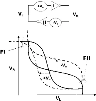
Fig. 1.12 Schematic of a CMOS SRAM cell during the standby mode and during the read access. The subscript "R" indicates the right side of the cell, the subscript "L" the left. The cell is more vulnerable at the noise during a read access [Fig 1 of [24]].
35 exponential subthreshold current.
Fig. 1.13 The static noise margin is defined as the minimum noise voltage present at each of the cell storage nodes necessary to flip the state of the cell. Graphically, this may be seen as moving the static characteristics vertically or horizontally along the si side of the maximum nested square until the curves intersect at only one point [Fig. 2 of [24]].
From Fig. 1.12 and Fig. 1.13 we can see how one can build two squares within the butterfly cell, whose you can produce the noise margins and SNML
36
SNMR. In order to evaluate the SNM in the worst case, the static noise margin
should be evaluated as follows:
(1.2)
The optimization of the static noise margin is one of the most important aspects in the design of SRAM cells[24]. One of the possible solutions to improve the scalability of SRAM cells, providing immunity to the fluctuations of the intrinsic parameters, is the technique of bias control. In [55], in particular, it focuses on the approaches of polarization of the bit line and the polarization of the gate of the access transistor.
Fig. 1.14 Mean value μ and standard deviation σ of the SNM as a function of the polarization of the bit line and the polarization of the gate of access transistor [Fig 4 of [55]].
37
noticeably the performance in terms of static noise margin. In fact, a decrease of 10% of the gate voltage of access transistor introduces an increase in the average value of the SNM () by about 18%. Note that the standard deviation () of the SNM decreases with decreasing gate voltage, with consequent benefits in terms of yield [55].
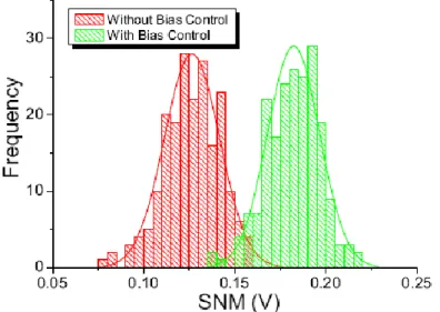
Fig. 1.15 shows the improvement of the static noise margin using a combination of the polarization of the bit line and the gate of the access transistor. In this way we can achieve improvements of over 40% of the SNM.
Fig. 1.15 Distribution of the noise margin with and without the control of the bias voltage [Fig. 5 del [55]].
38
At the device level, a proposed solution to alleviate the effects of intrinsic fluctuations [57] is to use the retrograde doping profiles in transistors and also use the channel lengths that are marginally larger than the minimum feature size. This alleviates the problem but does not eliminate it entirely. Circuit techniques that push away the tensions of the memory cell nodes from each other, improve the SNM of the cell, making it more immune to noise, are proposed in [58] as a solution that addresses the stability of the cell, the subthreshold leakage, and performance degradation in scaled CMOS SRAM.
39
2 State of the art
2.1 Random discrete dopant (RDD)
Wong and Taur were the first to propose a full 3D simulation of field effect transistors under the influence of random discrete dopants (RDD) [59]. They used a drift-diffusion simulator, which models the electronic transport as an incompressible fluid flow, considering the area under the gate like a checkerboard of smaller devices connected together, each with a different density of dopant atoms. The results show the two main effects of randomly distributed discrete dopants: a dispersion of the threshold voltage of the device, and a reduction of the average threshold voltage compared to the threshold voltage of the system with constant doping [4].
These 3D simulations prefigured the current techniques and used a 3D device simulator that is computationally efficient, but they were not taken immediately in commercial simulators. A 3D simulation requires significant computational resources; the simulations are even more important because of the need to have accurate models of atomic-scale lengths.
The dependence of the threshold voltage caused by the random fluctuation in the number of dopants in the channel of the MOSFET and of the random distribution at the microscopic level of atoms random discrete dopants in the channel of the MOSFET [59] has been studied, always using the drift-diffusion
40
approach, with the devices simulator FIELDAY [60]. Fig. 2.1 shows an example of a set of I-V curves of 24 MOSFETs with different random distributions of atoms for W = 50 nm, L = 100 nm, tox = 30 Å, and a uniform
doping average of the substrate of 8.6 × 1017 cm-3 . When compared it with the I-V characteristic of the same MOSFET simulated using the conventional continuous doping model, the simulation of discrete doping shows: 1) a dispersion of I-V curves along the axis of the gate voltage of about 20-30 mV, 2) a average shift of the I-V in the direction of the negative gate voltages of about 30 mV in the subthreshold region and about 15 mV in the linear region, and 3) a light degradation (<3 mV/dec) and fluctuation of the subthreshold slope. The shift of Vth in the subthreshold region is lower than in the linear
region due to the logarithmic dependence. The asymmetry of the threshold is about 20-40 mV, and this can be attributed to the discrete and random nature of the dopant atoms, resulting in an inhomogeneous channel potential [27].
41
Fig. 2.1 Drain current as a function of gate voltage for a conventionally doped MOSFET (circles) and 24 devices with different distributions of discrete dopants in the channel (gray lines). The current average of all 24 devices is indicated with triangles. The shift of the threshold voltage in the subthreshold region was defined as the shift of gate voltage to a level of constant current (Ioff) [Fig 18 of [27]].
Successively, Asenov et al. have carried out studies on the 3D atomistic simulations [61], [62]. For the first time was made of the systemic analysis of the effects of random doping in 3D on a scale sufficient to provide quantitative statistical predictions. It was adopted an approach to hierarchical atomistic simulations, always based on the drift-diffusion method. To reduce processing time and memory required for high drain voltages has been developed a self-consistent option based on a solution of the continuity equation of the current restricted to a thin slice of the channel. At low drain voltages, the single solution of the Poisson equation is sufficient to extract the current with satisfactory accuracy [61].
Dependencies and <Vth> (threshold voltage of the device with constant
doping profile) on the concentration of the dopants are compared in Fig. 2.2 for transistors with Leff = Weff = 50 nm and tox = 3 nm. The inset in the same figure
42
shows that the reduction of the threshold voltage induced by the random doping, increases almost linearly with increasing of the concentration of dopants [62]. In Fig. 2.3 is shown instead the dependence of
th V
of the same concentration.Fig. 2.2 Comparison of the dependence of the concentration of the dopants of <Vth> for transistor with Leff = Weff = 50 nm and tox = 3 nm.
43
Fig. 2.3 Comparison of the dependence of the concentration of dopants by calculated atomistically and the analytical models [45] and [63], with Leff = Weff = 50 nm and tox = 3 nm. Samples of 200 transistors [Fig 7 of
[62]].
In 2003, Andrei and Mayergoyz included quantum-mechanical effects in the analysis, suggesting a very fast technique for the calculation of the threshold voltage fluctuations induced by variations of the dopants [30]. This technique is based on linearization of the equations of transport in respect of the fluctuating quantities, and it is, from point of view computational, very efficient, since it avoids several simulations for various doping (as in the case of Monte Carlo techniques).
The results for the standard deviations of the threshold voltage obtained for a MOSFET with a channel length of 50 nm are shown in Fig. 2.4 and compared with those obtained by Asenov et al. for various oxide thicknesses. In [64],
th V
is calculated by simulating N = 200 MOSFETs, which implies errors of
th V
44
about
1
2
N
5
%
. The vertical bars in Fig. 2.4 correspond to the absolute value of these errors and show the range in which it has a probability of 68%. There is good agreement between the results extracted and those obtained using the statistical method in the case of classical computing. In the case of quantum calculations, the values are somewhat smaller than those reported in [64] due to the different electronic mass used in the simulations. The effective electron mass used in [64] mn* 0.18 is smaller than that used in these simulations, therefore, the values reported on, are approximately 15% larger.Fig. 2.4 Comparison of the with Asenov et al. [64]. The effective electron mass used in the simulations presented in [64] is
and it is different from the value used in [30], which justifies the difference in the calculations [Fig 5 of [30]].
By the comparison of data on the devices to 65 nm, can be seen that the RDF is about 65% of the total
th V
45 significantly lower channel doping.
Fig. 2.5 Variations of the transistor 65 nm and 45 nm, the data are compared with the RDF simulations under conditions of equivalent doping [Fig 4 of [7]].
Recently, Reid et al., using the Glasgow ―atomistic‖ simulator, have performed 3-D statistical simulations of random-dopant-induced threshold voltage variation in state-of-the-art- 35- and 13-nm bulk MOSFETs consisting of statistical samples of 105 or more microscopically different transistors [65]. Simulations on such an unprecedented scale has been enabled by grid technology, which allows the distribution and the monitoring of very large
46
ensembles on heterogeneous computational grids, as well as the automated handling of large amounts of output data.
The simulator self-consistently solves the nonlinear Poisson and current continuity equations in a drift diffusion approximation. The resolution of the individual discrete dopants is enabled by employing density gradient (DG) quantum corrections for both electrons and holes [66], [67].
The simulated 35-nm n-channel MOSFET (based on a device originally proposed by Toshiba) has a complex doping profile featuring retrograde indium channel doping and source/drain pockets [68]. The microscopically different devices in the >105 simulated statistical samples are generated using a continuous doping profile, which has been extracted from carefully calibrated process and device simulation using commercial TCAD tools [69]. The simulated 13-nm MOSFET is a scaled version of the 35-nm device, based on generalized scaling rules with structural parameters and doping profiles guided by the requirements of the ITRS, and represents a limiting case for conventional bulk MOSFET scaling [70][23].
In order to better understand the physical mechanisms whereby RDD affects Vth, the study the surface potential distributions of devices from close to the
mean, and from the upper and the lower tails of the distributions, at the identical gate voltages. There surface potential plots for both the 35- and 13-nm devices are shown in Fig. 2.6a and Fig. 2.6b, respectively. At both channel lengths, the behavior of the devices with higher Vth is determined by the clustering of the
dopants across the channel width at the location of the maximum of the potential barrier between the source and the drain. At this position, the dopants have the maximum impact on Vth by almost completely blocking the current
47
Fig. 2.6 Raw electrostatic surface potential profiles for the devices in the lower part, the middle, and the upper part of the distributions. (a) 35-nm devices, (b) 13 nm devices [Fig 6 of [65]].
In order to study the asymmetry in the Vth distribution induced by the
random dopant distribution, they have done a more detailed analysis to determine the statistically significant region (SRR) of the transistor that dominates the statistical behavior of the device ensemble. Moreover it is necessary to fix the number of dopants within the SSR (NSSR): this is possible
by estimating the distribution of the threshold voltage caused by the random partitioning of the dopants and calculating their mean and standard deviation.
From their analysis it becomes clear that the asymmetry in the random dopant induced threshold voltage distribution is due to factors: first, the Poisson distribution for a fixed value of NSSR is asymmetric with a positive skew, and
this asymmetry increases as NSSR is reduced, and, second, the standard deviation
48
This statistical analysis has identified the SRR of the devices, in which the number of dopants and their positions are closely correlated to the threshold voltage variation. The asymmetry of the distribution stems from the linear dependence of the mean and the standard deviation of the threshold voltage on the number of dopants in the statistically important region, as shown in Fig. 2.7.
Fig. 2.7 Dependence of the Vth mean and standard deviation as a
function of NSSR for both devices. The linear dependence allows the
positional effects on Vth to be extrapolated out to larger values of σ [Fig 10
of [65]].
2.2 Line edge roughness (LER)
The impact of line edge roughness (LER) on the performance becomes increasingly important with size reduction. In fact, due to the rapid technology development, the process of defining the gate are not yet mature and the LER is typically high [71].
49
be observed with the experiments comparing the currents of MOSFETs with different gate LER [73].
The experimental study of the doping profile and the extraction of relevant information from real devices is difficult and expensive and therefore almost exclusively numerical simulations are used [72].
The effects of LER depend on the technological process. In order to identify processes that provide intrinsic performance improvements, it is important to be able to separate the effects of LER by other factors.
In the ideal case, without taking into account the effects of LER, two transistors with the same gate length L, would have the same
I
on/
I
offgraphs. However, when including the effects of LER, the transistors, while having the same length L, are characterized by different edge profiles. The resulting dispersion of the characteristics could also cause a shift of the mean value compared to theI
on/
I
off ideal curve. In Fig. 2.8 the Gate LER of the gate in a traditional MOSFET is illustrated.50
Fig. 2.8 Illustration of a MOSFET with LER at the gate [Fig 1 of [72]].
Simulations for the study the LER are made using the approximation of a two-dimensional device [71]. The width of the transistor is divided in different segments of the two-dimensional devices with a width equal to the characteristic spatial period of the LER (called correlation length
), as shown in Fig. 2.9. Initially are determinedI
dsandI
off for each portion of the device and are then added together to obtain the ratioI
on/
I
off for the entire device.51
Fig. 2.9 A wide MOSFET with gate LER significant can be schematized with the parallel of many gate with equal width to the correlation length of the LER and gate length constant [Fig 1 of [71]].
Xiong et al. use a quick and convenient experimental method to extract and characterize the LER of the polysilicon gate [72]. This method consists in finding a controllable approach to produce a variable LER of the poly gate and integrate it into the process flow of MOSFET.
Software was then developed to extract the trends of the profile of the gate from the processing of data recorded on the poly lines using a scanning electron microscope (SEM). These measurements are performed on each line of poly (Fig 2.10).
52
Fig. 2.10 Extraction of the waveform of the line edge of the current data recorded by SEM [Fig 2 of [72]].
This method requires a large amount of data recorded by SEM, but does not require special tools for adjustment except for some considerations related to the resolution. The extent of the LER at this point can be obtained from analysis of the data that describe the shape of the contour of the poly. A Gaussian distribution cut at 3 dB can be used to approximate the statistical deviation of the edge. RMS values (indicated with
) of the profiles within the day are fairly consistent, if compared with the relatively large variations within the wafer.Xiong et al. found an effect of LER observable on the curves
I
on/
I
off.[72]. However, it was shown that this effect is significantly smaller than those caused by other changes in the process of the wafers where LER is generally quite small. With the help of numerical simulations it was noted that the main effect of gate LER on the device occurs in the doping profile. The scattering of dopant53
In 2001 it was proposed an analytical model of the LER [73], which has thus provided an efficient and accurate estimation of the effects related to it.
It is possible to distinguish two types of LER: short radius and long radius. The short radius LER has a high spatial frequency (i.e., a characteristic length of ~ 1 nm) and it is mainly attributable to the conditions of the lithography process and of the resist. On the other hand, we speak of long range LER for characteristic lengths greater than 10 nm; this type of LER is mainly due to surface roughness of polysilicon. The Tab. 2.1 summarizes the impact of various lithographic processes on the LER.
Tab. 2.1 LER for 100-nm resist lines [Table II of [73]].
LER-induced variability has been the subject of numerous modelling and simulation studies of different degrees of complexity and sophistication. The use of 2-D simulations of devices with different channel lengths in combination with the statistics of different channel length occurrences in the presence of LER has been popular due to the low computational burden [74], [75].
54
Comprehensive 3-D simulations vary in the complexity of the LER description from square wave approximations [76], [77] to realistic statistical descriptions of the gate edge based on different autocorrelation functions fitted to experimental LER data [78]. More sophisticated 3-D simulation studies include the confluence of LER and atomic-scale process simulation [79] and the impact of LER-induced strain variations [80]. However, a common denominator in all of the published 3-D simulations studies is the relatively small statistical sample, which rarely exceeds 200 microscopically different devices.
In [81], Reid et al. present a comprehensive 3-D simulation study of LER-induced MOSFET threshold voltage variability using statistical samples of more than 104 transistors. Contemporary, bulk, ultrathin-body (UTB) SOI, and double-gate (DG) MOSFETS have been simulated and analyzed. The large size of the simulated statistical samples allows accurate estimation of the higher order moments and the shape of the distributions of Vth. Intensive statistical data
mining is also used in order to explain the specific shape of the simulated distributions.
The simulations presented in [81] were carried out using the well-established Glasgow 3-D ―atomistic‖ statistical device simulator [23]. Random gate LER patterns are introduced into the simulations using 1-D Fourier synthesis, as described in [78]. A Gaussian autocorrelation function characterized by an RMS amplitude (Δ) and correlation length (Λ) has been adopted to describe LER, as in previous LER simulation studies [78]. In all simulations reported in [81], values of Δ = 1.6667 nm and Λ = 30 nm have been used to generate random source/drain and gate edges introduced by roughness of the resist and the following gate patterning process. This corresponds to LER patterns with magnitude 5 nm, which is representative of the state-of-the-art 193 nm
55
contemporary CMOS technology, where laser scan annealing is progressively applied for doping activation.
In order to confirm the trends observed in the simulations of the bulk 35-nm MOSFET, and to examine the potential impact of LER on different device architectures, smaller ensembles of three other devices have been simulated. The selection includes an LP 42-nm physical gate length bulk MOSFET with an oxide thickness of 1.7 nm, developed by ST Microelectronics and described in detail in [83]; a 32-nm physical gate-length UTB SOI MOSFET with a body thickness of 7 nm and equivalent oxide thickness (EOT) of 1.2 nm; and a 22-nm DG MOSFET with a body thickness of 10 nm and EOT of 1.1 nm. The last two devices were developed by the PULLNANO consortium [84] and are described in detail in [85]. The distributions of threshold voltage for 35- and 45-nm bulk; 32-nm SOI and 22-nm DG devices at low drain voltage (VD = 100 mV) are presented in Fig. 2.11. For all devices, the shape of the distribution of Vth is
similar and all are negatively skewed. It should be noted that the SOI MOSFET in particular exhibits good immunity to LER-induced variability, having a standard deviation of Vth that is much lower than the other three devices. This is
56
Fig. 2.11 Comparison of the distribution of Vth due to LER in the four
simulated devices at VDS = 100 mV [Fig 8 of [81]].
The skew and kurtosis values for the four simulated devices are given in Tab. 2.2, along with the other moments of the statistical distributions. The values of the moments also confirm the visual observation that the SOI device has significantly better immunity to LER-induced fluctuations.
57
voltage is asymmetrical with a negative skew, which increases with drain bias. There is a very strong nonlinear correlation between the threshold voltage and the average channel length of the LER transistors that very closely follows the channel length dependence of the threshold voltage in transistors with uniform gate edges. Increasing the channel width reduces the threshold voltage standard deviation more slowly than
1
W
and improves the symmetry of thedistribution of threshold voltage. The asymmetry of the distribution and the strong nonlinear correlation between the threshold voltage and the average channel length was also confirmed in the simulation of a 42-nm physical channel-length bulk LP MOSFET, a 32-nm channel-length thin-body SOI MOSFET, and a 22-nm channel-length DG MOSFET [81].
2.3 Oxide
thickness
variation
(OTV)
or
Surface
Roughness (SR)
In past years, the threshold voltage fluctuations induced by random variations of oxide thickness have not received the same attention to fluctuations induced by random doping. However, Andrei and Mayergoyz in their analysis [30], considered in addition to the threshold voltage fluctuations induced by variations of the dopant (RDD), even those induced by the oxide thickness variation (OTV).
58
The surface oxide was initially characterized by a Gaussian autocorrelation function. However, measurements made more recently have shown that fluctuations in the oxide thickness are better described by a distribution function of exponential type [30].
Asenov et al. have studied the intrinsic threshold voltage fluctuations introduced by local variations in oxide thickness (OTV) in decanano MOSFETs, using three-dimensional numerical simulations on statistical scale [12]. Si/SiO2 random interface is generated by the power spectrum
corresponding to the autocorrelation function of the interface roughness. The simulations showed that the intrinsic fluctuations of the threshold voltage induced by OTV become significant when the device size becomes comparable to the correlation length
of the interface.The dependence of
th V
by the average oxide thickness is shown in Fig. 2.12; in the simulations has considered only the Si/SiO2 interface roughness. Thistrend is related to the linear dependence between Vth and tox, resulting in a
59
Fig. 2.12 Dependence of threshold voltage standard deviation of the average oxide thickness <tox> for a 30 × 30 nm
2
MOSFET with a random Si/SiO2 interface [Fig 6 of [12]].
The Fig. 2.13 shows the dependence of the mean threshold voltage <Vth> vs.
<tox> calculated from classical and quantum method, for Λ = 10 nm. For
comparison the dependence of the threshold voltage Vth of the device with
uniform oxide thickness (tox) is plotted as a function of tox. It is clear that the
threshold voltage <Vth> of the device with random thickness is very close to the
corresponding threshold voltage of the MOSFET with uniform oxide. The slight reduction of <Vth> in the classic case is associated with the increase of the
current density at the boundaries between the regions of thinner oxide and thicker region due to the effects of the intensification of the field [12].
60
Fig. 2.13 Dependence of the average threshold voltage < Vth > from the
medium thickness oxide <tox> for a 30 × 30 nm2 MOSFET with a random
Si/SiO2 interface (symbols) and of the threshold voltage Vth on the oxide
thickness tox for a similar device with uniform oxid (lines) [Fig 7 of [12]].
2.4 Combined effects
Asenov et al. carried out some 3D simulations to study the dispersion of the intrinsic parameters, not considering only the effects individually, but also the combined effects of RDD, LER and OTV on the fluctuations of the threshold voltage [23].
The study of the fluctuations of the threshold voltage was done using 3D drift-diffusion simulations (DD). The DD approximation does not capture the effects of the non-equilibrium transport of carriers and therefore underestimates the drain current in the ON state. However, this is adequate for the calculation
61
"Density Gradient" implemented in the simulator capture well the effects associated with the direct source-drain tunneling, which become apparent in the channel lengths of 10 nm, and accurately reproduces the results of simulations of the non-equilibrium Green's function (NEGF).
In the case of RDD simulations, the generation of distribution of random doping is based on continuous distribution of dopant obtained from the whole simulation process of the device of reference and of the scaled device: all sites in the lattice of silicon that covers the simulated device are controlled one by one. The dopants are introduced randomly in sites with a probability given by the corresponding dopant concentration ratio of silicon, using a rejection technique. Each dopant is assigned to the eight surrounding nodes of the grid using the cloud-in-cell technique (CIS) commonly used in Monte Carlo simulations.
With less than 10 dopants in the region emptied of the channel of most of the simulated devices, the resolution of each individual dopant becomes very important. However, the resolution of individual charges in the simulations "atomistic" using a dense grid creates problems. Due to the use of Boltzmann statistics or Fermi-Dirac in the approach to drift-diffusion classic, the electron concentration follows the electrostatic potential obtained from the solution of the Poisson equation. Consequently, a significant amount of mobile charge can be trapped (localized) in Coulomb potential wells created by discrete dopants assigned to the dense grid. The trapped charge artificially increases the
62
resistance of the source-drain regions and change the depletion layer that results by the reduction of the threshold voltage. Another damaging effect of this trapping of charges in classical simulations is the strong sensitivity of the amount of charge trapped on the size of the grid.
If using a denser mesh, you get a solution to the single Coulomb potential well and increases the amount of trapped charge.
Attempts were made to correct these problems in the "atomistic" simulations both with the charge distribution on more grid points and with the decomposition of the Coulomb potential in the short-and long-range components, based on considerations of screening. The charge-smearing approach is however purely empirical and may result in a loss of resolution on the effects of "atomistic" scale. The splitting of the Coulomb potential in the short and long range components suffers from some disadvantages including the arbitrary choice of cutoff parameters and for double counting of the potential of screening of the mobile charge.
Typically the approach adopted in the "atomistic" DD simulations is the DG approximation. Typically, for example, in the DG simulations of n-channel MOSFETs, this is enough to solve the Poisson equation self-consistent, the current continuity equation for electrons and the equation of state for electrons written in approximation DG.
(2.1)
where
![Fig. 1.1 The time progresses of Moore's law [1].](https://thumb-eu.123doks.com/thumbv2/123dokorg/7557350.110080/10.722.114.568.106.429/fig-time-progresses-moore-s-law.webp)
![Tab. 1.3 Emerging Research Material Technologies Difficult Challenges [3].](https://thumb-eu.123doks.com/thumbv2/123dokorg/7557350.110080/15.722.121.633.99.683/tab-emerging-research-material-technologies-difficult-challenges.webp)
![Fig. 1.10 Delay vs. δV th for an inverter [Fig 3. of [8]].](https://thumb-eu.123doks.com/thumbv2/123dokorg/7557350.110080/34.722.193.530.114.435/fig-delay-vs-δv-th-inverter-fig.webp)
![Fig. 2.3 Comparison of the dependence of the concentration of dopants by calculated atomistically and the analytical models [45] and [63], with L eff = W eff = 50 nm and t ox = 3 nm](https://thumb-eu.123doks.com/thumbv2/123dokorg/7557350.110080/45.722.215.544.111.389/comparison-dependence-concentration-dopants-calculated-atomistically-analytical-models.webp)
![Fig. 2.10 Extraction of the waveform of the line edge of the current data recorded by SEM [Fig 2 of [72]]](https://thumb-eu.123doks.com/thumbv2/123dokorg/7557350.110080/54.722.125.603.114.395/fig-extraction-waveform-line-edge-current-data-recorded.webp)
![Fig. 2.11 Comparison of the distribution of V th due to LER in the four simulated devices at V DS = 100 mV [Fig 8 of [81]]](https://thumb-eu.123doks.com/thumbv2/123dokorg/7557350.110080/58.722.169.548.114.389/fig-comparison-distribution-ler-simulated-devices-ds-fig.webp)
![Fig. 2.14 Doping profiles of the one-dimensional channel of the MOSFET calibrated at 35 nm and of the scaled devices with gate length of 25, 18 , 13, 9 nm [Fig 3 of [23]]](https://thumb-eu.123doks.com/thumbv2/123dokorg/7557350.110080/67.722.205.559.100.369/doping-profiles-dimensional-channel-mosfet-calibrated-scaled-devices.webp)
