Università degli Studi di Catania
Dottorato di Ricerca in Fisica
XXIV Ciclo
Antonio Massimiliano Mio
Crystallization of Amorphous Chalcogenide
Nano-Regions and Test-Structure Fabrication
for Non-Volatile Memories
Tutor:
Prof. E. Rimini
Prof.ssa M.G. Grimaldi
Supervisor:
Dr. Giuseppe D’Arrigo
Coordinatore: Prof. F. Riggi
Tesi per il conseguimento del titolo
Crystallization of Amorphous Chalcogenide Nano-Regions and Test-Structure Fabrication for Non-Volatile Memories
Antonio Massimiliano Mio
Ph. D. Thesis – Università degli Studi di Catania Printed in Catania, December 2011
i
Contents
Introduction ... 1
Phase Change Material characteristics ... 7
PCM-based memories: main designs and electrical characterizations ... 16
Motivation ... 23
Chapter 1 ... 27
1 Nucleation and grain growth in as deposited and ion implanted GeTe thin films ... 27
1.1 Ion Implantation in chalcogenide thin film ... 28
1.2 Comparison between as deposited and ion implanted amorphous GeTe by Optical Microscope ... 34
1.3 Comparison between as deposited and ion implanted amorphous GeTe by TRR measurements. ... 42
1.4 The JMAK Model ... 45
1.5 Comparison between TRR and Optical Microscopy in situ measurements ... 48
1.6 An insight on the different amorphous structures by means of Raman Spectroscopy measurements ... 51
ii
Chapter 2 ... 59
2 Fabrication and characterization of amorphous nano-structures of Ge2Sb2Te5 for amorphous to crystalline transition study ... 59
2.1 Fabrication of nano structures by Electron Beam Lithography .... 61
2.1.1 Nano-apertures ... 62
2.1.2 Nano pillars ... 66
2.2 Ion Beam Implantation in nano-apertures ... 72
2.3 In situ annealing of nano amorphous structures by Transmission Electron Microscopy ... 76
2.3.1 Embedded nano amorphous regions ... 76
2.3.2 Isolated nano amorphous pillar ... 94
2.4 Comparison between present results and device configuration .. 98
Chapter 3 ... 100
3 Fabrication and characterization of Phase Change Memory test structures ... 100
3.1 Ge2Sb2Te5 thin film annealing for device fabrication ... 104
3.2 Ge2Sb2Te5 lithography and patterning ... 108
3.3 Electrical Characterization ... 115
3.3.1 Bench setup ... 115
3.4 Programming and sensing of bridge cell memory ... 119
3.5 Discussion and Future Perspective ... 129
iii
Bibliography ... 134
List of publications ... 142
Conferences ... 143
1
Introduction
The modern semiconductor technology, following the road map based on the Moore’s law, has pushed CMOS-based electronic devices towards smaller and smaller dimensions, until reaching the 22nm node, indicating the minimum half distance between two devices in a chip. The scaling of the device dimension has increased the system functionality (e.g., more GBytes for memories or higher clock velocity for CPUs) that can be delivered in the same size package. Actually these improvements are both a byproduct of, and the driving force for, the relentless march to smaller device dimensions predicted by Moore [1].
Figure 1 Moore’s Law. The chart tracks the progress of transistor integration, for Intel’s devices, from 1960 to 2010.
Introduction
2
The history of the semiconductor industry has been dominated by this concept: higher densities at similar cost lead to more functionality, and thus more applications, which then spur investment for the additional research and development needed to implement the next size smaller device. Throughout this extensive history, extrapolation from the recent past has proven to be amazingly reliable for predicting near future developments. In almost 60 years this history has been correlated to that of silicon, that has shown its predominant characteristics with respect to the other semiconductors, in terms of intrinsic features, integration with other materials, manipulation of its properties and scalability. From the beginning of silicon-based electronics, with the progression described by Moore, lithographic technological progress has permitted to decrease the typical feature size of order of magnitudes, from hundreds of microns to tens of nanometers. Nevertheless, this huge difference in dimension has not implied severe change in device layouts but essentially their rescaling, because the more relevant semiconductor properties are independent of the size until the submicron scale. Moreover, this is the main reason why, in the past century, the study of the material properties has been mainly addressed towards the bulk characteristics of the material itself, without particular concerning to its dimension.
However, as the dimension of the device becomes smaller than 22nm, the extrapolation of the properties obtained by the experimental data on bulk materials to nanosize structures, and then simple rescaling of the device layouts, is not, a priori, a correct procedure. As the size gets smaller the system is affected by several effects. First, the large extension of the crystal and its periodicity fall and so the Block theorem and the band model are not still valid to describe the system. Quantum size effects take place and discrete levels appear in the crystalline momentum corresponding to the shrunk directions. If the energy level distances are of the order or greater than kT, electrical and optical properties suffer this new state arrangement. Level distances and shift depend on the chemical characteristics of the
Introduction
3
crystal and on the strength of Coulomb interaction between almost free-electrons in the crystal and atomic potential.
In semiconductor, for instance, these effects are rather relevant with respect to the metals. Increasing the system size of a generic crystal, in fact, the number of levels increases at first in the center of the band and then at the edge.
As a consequence, in metals, where the Fermi level lies in the middle of a band, the relevant energy level spacing is still very small even in relatively small sizes (tens or hundreds of atoms) [2-4]. At temperatures above a few kelvin, the electrical and optical properties, therefore, more closely resemble those of a continuum. In semiconductors, instead, the Fermi level lies between two bands, so that the edges of the bands dominate the low-energy optical and electrical behavior.
Many works have demonstrated, both theoretically and experimentally, the relevance of the quantum size effects. Moreover, recent studies also take into account further properties emerging with scaling as absence of electron scattering in the so called mesoscopic-ballistic regime. Furthermore, while in the bulk materials transport is quite insensitive to the amount of carriers in the system, in nano structures, Coulomb Blockade shifts the energy levels as electrons are stored. These effects modify the behavior of the elemental components in a chip, requiring, at least, a further investigation about their global behavior in a combined layout. Together with the scaling problem intrinsic of the shrinking of the silicon structures and then with the radical change in its electro-optical properties, other relevant problems regards the insulators involved in the CMOS (Complementary Metal Oxide Semiconductor) operation, especially memories. With scaling, in fact, the amount of electrons stored in the floating gate in a Flash memory reduces, until the signal to noise ratio becomes too small. Nevertheless, stress-induced leakage current (SILC) can occur across ultra-thin oxides CMOS-based memories by programming it
Introduction
4
with large voltages. Also one must to maintain coupling between the control and floating gates and to avoid the cell-to-cell parasitic interference between the stored charge in closely-packed cells[5-7].
The huge storage capacity the market requires could be provided by Silicon-based Multi-Level Cells (MLC), associating to the same cell different analogical states. However, since performance of MLC is worse than Single-Level Cell by means of programming speed, data retention and endurance, prototypal memories have not been commercialized in Flash-based SSD [8]. For these reasons, new kinds of memories, satisfying at the same time programming performance, endurance and, overall, scaling capability must be found.
New Non Volatile Memories (NVMs) candidate technologies are, at now, under consideration to substitute Flash Memories. Basically, there are two different kinds of approach. The first one consists of building memories that have a very simple integration with the consolidate CMOS technology; this is the case of ferroelectric and magnetic RAM. The other approach is to consider a completely new concept as in the case of racetrack memory and organic RAM. However, in the latest case, the research is still at beginning, mainly consisted by proofs of concept. Another class of memory considers something in-between with respect to these two concepts and this is the case of Phase Change Memories (PCM), resistance RAM, and solid-electrolyte memories [9].
Naturally, together with the performance requirements, they also need to be scalable for more than a decade, to justify the investments needed to develop a new technology.
Fortunately, Phase Change Random Access Memories (PCRAMs), in which the information bit is associated to the different resistivity of amorphous and crystalline phases, offer very good scalability perspective, both from preliminary studies on ultra-thin films (few nanometers) and from sub-lithographic prototypal devices. Good performance devices have been, in
Introduction
5
fact, recently demonstrated with a cross-section as small as 113 nm2 [10] in isolated cell of about 3400 nm3.
However, although many long terms issues have been predicted and solved, some others need a deeper research study, such as MLC with 4 bits per cell or the reduction of the RESET current, that represents the higher current experienced by a PCRAM, for technology node beyond 28nm (Figure 2).
Figure 2 PCRAM present and future requirements, as defined by the International Roadmap for Semiconductor 2010 [11]. According to the severity of the improvement a white, yellow or red box is used in correspondance of the proposed value.
The information bit, in these memories, is associated to the resistance of the crystalline and of the amorphous phases. In fact, a huge difference in resistivity (until to 6 order of magnitudes) between them occurs for chalcogenide. The material can easily be switched between these two state by current pulses of few hundreds A with typical widths ranging from 10 to 100 ns.
Introduction
6
Since their features strictly depends on the retention of the metastable disordered phase and on its characteristics, many studies have been conducted in amorphous thin films to investigate the crystallization kinetics [12-14].
However, as the dimension of the amorphous region gets smaller, the crystallization process, produced by the nucleation of crystalline grains followed by their growth, slows down since statistical occurrence of nucleation events drastically decreases. In addition, extrapolation of blanket properties data fails for different reasons. First, nucleation in chalcogenides is heavily influenced by surface, being in most cases heterogeneous. Second, amorphous active regions in devices are often surrounded by crystalline phase, reducing their stability, since no nucleation occurrence is required to start crystallization. Finally, amorphous formation, arising in device, comes with a great change in density (about the 6%) producing local stress in the memory cells. This compressive stress probably reduces the crystallization kinetics [15-16].
For these reasons, amorphous behavior in PCM must be studied in nano systems, in a closely condition with respect to the device active region.
7
Phase Change Material characteristics
As previously noted, market requires memory devices of smaller and smaller sizes. However, together with this main requisite, different prerequisites must be also satisfied. These prerequisite can be summarized in speed, SET-RESET contrast, endurance, ciclability and data retention. Assume a SLC system in which a memory element switches its state between only two possible levels: a reset state, also indicated by “0”, to a set state “1” and viceversa. Speed regards the velocity of switching between these two states; SET-RESET contrast concerns the difference between the read physical values in the two states: as large is this difference as fast it is possible to readout information upon the noise; endurance and ciclability regard how this difference is maintained with time/operations and how many set/reset cycles a cell can sustain before it fails; finally data retention concerns how much time bit information is maintained at a given temperature.
The way in which Phase Change Random Access Memories (PCRAMs) satisfy these requirements, strictly depends on the working principles they operate. Basically, the working principle of these devices is based on the substantial difference between the electrical properties of the amorphous and crystalline phases. Crystalline phase is a high conductivity state while the viceversa occurs in the amorphous state. Moreover, since these two phases present a relevant difference in reflectivity, chalcogenide are also largely used for high-density data storage in optical media (CD-RW, DVD-RAM, DVD-RW, Blu-ray Discs). The reflectivity contrast between these two states is about 30%, while the resistivity difference can reach up to six orders of magnitude (for instance in GeTe). Since these two conditions can be clearly distinguished (by a low power laser pulse for reflectivity or by a
Phase Change Material characteristics
8
low power current pulse for resistivity) one can associate straightforwardly a bit information to it.
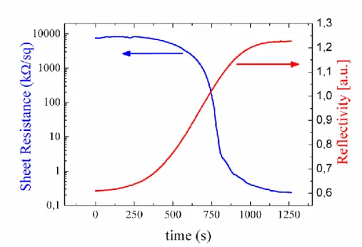
In Figure 3, time resolved measurements of sheet resistance and reflectivity have been reported for an amorphous GeTe film during its crystallization by in situ annealing at 167°C.
Figure 3 Time resolved measurements of sheet resistance and reflectivity for an as sputtered amorphous GeTe film (40 nm thick) during in situ annealing at 167°C. By crystallization the film resistivity decreases of several order of magnitudes and the reflectivity significantly enhances.
In Figure 4, the key points of phase change memory operation are summarized. Conventionally, the crystalline phase is related to the SET state and with SET operation we mean the process by which an amorphous bit of memory is transformed in a crystalline one. The viceversa occurs for RESET state and the involved RESET operation. In the optical recording system, reversible phase changes between crystalline and amorphous
Phase Change Material characteristics
9
phase are achieved by short laser pulses with duration of tens of nanoseconds: the material is brought above the melting temperature and then, rapidly quenched by the surrounding environment (109 K/s).
Figure 4 Operation involving phase change memories [17]. To set a device into the crystalline set state indicated by “1” (green) a (laser or current) pulse heats the system bringing it in the regime of fast crystallization (red). To reset the device, bringing it in the “0” amorphous state (orange), a pulse heats the system above the melting point. From the rapid quenching of the liquid, the system amorphizes. A low power pulse, small enough to
Phase Change Material characteristics
10
avoid material modification for the reset or set operation, is applied in order to read the reflectivity or the resistivity state.
The liquid phase, in this condition, has not enough time to rearrange in the crystalline phase and the liquid is frozen in the amorphous, disordered, phase. Current pulses of the same duration generate the phase switching in non-volatile electronic memories, following the same quenching mechanism. Crystallization occurs, instead, in solid phase by longer, less energetic, pulses since the transformation temperature is intermediate between those of glass formation and melting, in the so-called regime of fast crystallization. Hence, in the write and reset operations, the crystallization limits the operation frequency, usually about 10 MHz, and so the speed requirement.
The most frequently used chalcogenide alloy in NVM is certainly Ge2Sb2Te5
(GST). Studies so far have shown that GST has one of the best combinations of electric and phase changing characteristics for PCRAM applications [18-20]. It is known that, in planar amorphous thin films, the phase transition of as-deposited amorphous Ge-Sb-Te alloys proceeds, during annealing, to the metastable face centered cubic (fcc) rock-salt phase (155°C) and to the stable hexagonal close packing (hcp) structure (350°C) by nucleation and growth of the different phases [13, 21, 22]. Figure 5 (a) and (b) indicates, respectively, these two crystalline phases. In particular, the rock-salt phase has been shown to be divided in two fcc sublattices. One fcc structure is occupied by Te atoms. The other fcc is randomly occupied by Ge and Sb atoms and vacancies (20% of the sublattice).
Chalcogenides, and in particular GST, represent a viable alternative to silicon in the non-volatile memory sector because they show good data retention, excellent switch velocity and miniaturization aptitude. The coexistence of these requirements is made possible by the particular amorphous structure they have, not so different to the crystalline state, that makes easier the switching between these two phases. Several models [23][24][25] have been proposed to describe this property. In particular,
Phase Change Material characteristics
11
one pictorial phase-change mechanism, has been proposed by Kolobov et al. consisting of the so-called umbrella-flip in which Ge atoms change their symmetry from the amorphous tetrahedral configuration to the rocksalt-crystalline octahedral one (Figure 5c).
Figure 5 Ge2Sb2Te5 in its crystalline phases: (a) fcc and (b) hcp [26]. In (c) it is shown a possible fcc-amorphous mechanism of transition, the umbrella flip, in which a Germanium atom (indicated in red) changes its symmetry from the amorphous tetrahedral configuration to the crystalline octahedral one [23].
Phase Change Material characteristics
12
Recently it has been pointed out [27], by ab-initio simulations and Raman spectroscopy, that amorphous phase in chalcogenides can be ascribed to a defective octahedra environment in which the crystalline sixfold coordination of Ge atoms in crystalline state is not fully established. By ab-initio simulations [25] it has been also shown the presence of a crucial structural motif of misaligned ABAB squares in amorphous GST (A=Ge,Sb for GST, and A=Ge for GeTe; and B=Te), which can straightforward rearrange to the crystalline configuration.
In spite of the straightforward mechanism involving phase transition in chalcogenide, amorphous structure must exhibit good stability (high data retention) connected to high glass temperature and, at the same time, low programming power (and current) connected to a low melting point. Matching these two requirements is not trivial: many research attempts in chalcogenide materials are focused to modify the alloy composition toward this direction [28]. On the other hand an important open quest in chalcogenides regards the crystallization thermodynamics and kinetics from the metastable amorphous phase, varying the dimension of the system. Another important subject in devices regards the presence of the crystalline phase around the active region of the devices that can compromise the amorphous stability. Almost all PCM layouts present this configuration, apart from some particularly prototypal device [10] in which the active region is isolated.
As sizes get smaller, the number of the surface atoms plays a relevant role with respect with the total number of atoms. In any material, surface atoms make a distinct contribution to the free energy, and the large changes in thermodynamic properties of nanocrystals (melting temperature decreasing , solid-solid phase transition temperature increasing) are commonly ascribed to the minor amount of bonds that atoms in the surface have.
Phase Change Material characteristics
13
Therefore, reducing the dimension we have a minor amount of bonds per atom we have to break for melting, thermodynamical stability of the structure is reduced and, as a consequence, melting point decreases. However, the behavior of the crystallization temperature is not a-priori well-defined. Different results, according to the material and to its surrounding surfaces, have been obtained as its size decreases. For instance, for the GeSb alloy [29] the crystallization temperature increases in a blanket film as its thickness gets smaller in the range between 7.0 and 1.3 nm. It has been also fabricated, by Electron Beam Lithography, an array of 20-40 nm isolated nanopillar from a 50nm GeSb film, reducing in the nanometer scale all the dimensions. In this case, crystallization temperature slightly decreases (about 15°C) as the nanopillar size decrease (from 50nm to 20nm), indicating an opposite behavior. To our knowledge, similar experiments on GST have been performed only for thin films. The same authors also indicates an increasing of the crystallization temperature for the amorphous-fcc transition as the GST films get thinner in the 19.0 – 1.3 nm range, and in particular no rock-salt transition has been observed below 3.6 nm. No variation of crystalline temperature has been detected in the same thickness range for the transition to hexagonal, while, abruptly, no transition has been observed at 1.3 nm.
Wei et al. [30] also confirmed a similar behavior in the 20÷5 nm thickness range, proposing a model based on thickness dependent interfacial energy. When film thickness decreases the role of the crystalline grain in the interface becomes predominant. The increasing interfacial energy causes the nucleation barrier enhancement and thus crystallization temperature increases. The increasing of the glass temperature, decreasing the structure dimensions, offers optimistic expectation concerning the devices scalability, providing an important prediction about the improvement of the data retention performance. As a matter of fact, several kinds of PCRAM devices have been fabricated [31] in the last years with data retention better than 10 years at 100°C [34].
Phase Change Material characteristics
14
The properties of chalcogenide amorphous materials, however, not only concern system dimension. More generally, in fact, in a glass material, an infinite kinds of amorphous phases exist, depending on quenching rate, deposition method, amorphization technique [33, 34, 35] and each amorphous state reasonably presents a peculiar kinetics behavior.
In particular, we can consider three different kinds of amorphous structures: the as deposited, the melt-quenched and ion implanted ones. The first is produced by deposition method itself, usually by the (RF or DC) sputtering action of an Ar-based Plasma on a stoichiometric target. Although the target is usually crystalline, if the deposition temperature is maintained below the chalcogenide glass temperature, the resulting film will be amorphous. Melt-quenching is the mechanism aforementioned involving the optical and electronic memories and then it refers to an amorphous originated from a liquid phase. Finally, the third kind of amorphization can be accomplished by ion irradiation. Ion bombardment, in fact, at suitable energies (tens of keV) and fluencies (≈1014 ions/cm2) can displace atom in the host target to random positions, producing disorder. Each ion impinging in the chalcogenide produces a collision cascade with a typical radius of about 10 nm. According to the thermal and atomic diffusivity of chalcogenides, the collision cascades regarding ion bombardment in the material can be correlated with a local thermal spike annealing of about 10 ps [36] at temperatures very close to the melting point.
A full comprehension of the differences connected to these three kinds of amorphous phases is still missing and, nevertheless, necessary. Recent experiments [36, 37] and atomistic simulations [34] have been focused on the different crystallization behavior between them, pointing out difference in their local order arrangements. In particular, it has been shown that deposition process causes wrong bonds formation, i.e. homopolar bonds not allowed in the crystalline phase, acting as an obstacle during the crystallization.
Phase Change Material characteristics
15
As we will show in chapter 1, a reduction of the homopolar bonds (e.g. Te-Te bonds in GeTe-Te), occurs during ion implantation or melt-quenching with respect to the deposited amorphous. As a consequence amorphous produced by melt-quenching and by low fluencies i.i. are similar in crystallization kinetics, as previously reported [37] by means reflectivity measurements, while slower crystallization rates has been observed in as deposited sputtered films.
16
PCM-based memories: main designs and electrical
characterizations
Several kinds of PCM-based memory devices have been proposed and successfully fabricated. Among the different designs, however, the aim of the present work is to confine the heating profile of the region in which the active storage material of the cell resides, in order to bring it easily in the melting region or in the regime of fast crystallization (Figure 4). To obtain this result, memory cell must be addressed in proximity with the electrodes. The two principal cell archetypes are reported in Figure 6.
Figure 6 Phase-change device archetypes: (a) A typical contact-minimized cell, the mushroom cell, forces current to pass through a small contact formed by the intersection of one electrode and the phase change material [26]. (b) A typical bridge cell confines the active volume of the phase change material in a line between two TiN electrodes [38].
PCM-based memories: main designs and electrical characterizations
17
Figure 6a shows a mushroom cell. From a Bottom Electrode Contact (BEC) current is delivered towards the device through a tight via in order to increase current density and resistivity in the proximity of the metal-chalcogenide interface. Finally current reaches the Bit Line, that represents the Top Electrode Contact (TEC). Different materials can be used in the BEC in order to engineer the local resistivity and to enhance the Joule heating near the PCM. Generally, however, a Tungsten-based alloy is preferable, due to its high melting point (≈3700 K). Figure 6b illustrates a Scanning Electron Micrograph of a phase change bridge cell between two TiN electrodes. In this configuration, current is confined in the tight line (few tens of nanometers). The configuration in a) is preferred for the final industrial fabrication, because it can be easily inserted in high dense memory cell array. Configuration b), however, is more suitable to exploit the PCRAM behavior and characteristics, because of the easily access to the active region of the device (that is usually under a unique passivation film, instead of several layers) that permits morphological, structural and chemical analyses. Moreover, since one of the dimension involving the cross section in which current flows is the thickness, the bridge configuration allows scalability below the lithographical current node, permitting also predictions about future devices. Several works [39] are devoted to simulate the thermal profile, produced by Joule heating, in PCRAM during programming. Figure 7a shows the results obtained by Kim et al. referred to a mushroom cell during reset operation. Simulation assumes adiabatic and convection boundary conditions in the heat diffusion model. Over the BEC, temperature can reach the melting point of the chalcogenide material (about 916 K in Ge2Sb2Te5). With rapid quenching
(≈10 ns, with a cooling rate ≈109 K/s) an amorphous dome is produced, with the typical mushroom shape (Figure 7b). Again, Joule heating is responsible of the crystallization of the amorphous dome in the SET operations. However, while addressing a large amount of current is straightforward in a SET crystalline state, due to its low resistivity, in principle, we need large voltage values to obtain significant currents in an amorphous, high
PCM-based memories: main designs and electrical characterizations
18
resistivity, state. The suitability of chalcogenide materials as electronic memory resides, instead, in their capability of changing their conductivity in the amorphous phase from an high resistivity to a conductivity state at a certain electrical field value. This mechanism, demonstrated by Ovshinsky in 1968, is called threshold switching [41].
Figure 7 Simulation of the thermal profile [39] in a mushroom cell during RESET operation. Over the Bottom Electrode Contact (BEC) temperature overcomes the melting point and, from quenching, an amorphous dome is obtained (b) [40].
Peculiar I-V characteristics of a PCM cell can be obtained by voltage sweep up, typically from 0V to 2÷3 V, with ≈100ns long pulses. In Figure 8, this procedure is shown for a SET cell (full squares) and for a RESET cell (empty circles).
The SET state features a slight non-linear I-V (Figure 8) curve with a resistance varying between a low-field, low-current, regime (OFF state) and a high field, high-current, regime (ON state). For both these states the resistance measured during the pulse is usually in the KOhm range. The RESET state is characterized by a significant larger resistance in the low-field
PCM-based memories: main designs and electrical characterizations
19
regime, usually in the range of few MOhm. However, the I-V curve suddenly changes at the threshold voltage ( in the figure) where the conductivity
of the cell becomes comparable to that of the set state. This transition is known as threshold switching. Without the threshold switching mechanism, ≈10V should be applied to the PCM cell to deliver an amount of power suitable for cell crystallization. Such high voltage value would be incompatible with those operating in a CMOS addressing system.
Figure 8 Experimental I–V curve of a mushroom cell with the GST in the crystalline and in the amorphous state. It is obtain by sweep up an amorphous (empty circles) or a crystalline (full squares) state. Threshold switching at and relative snap back are
clearly visible. Typical voltage regimes for reading (READ), setting (SET) and resetting (RESET) are also emphasized.
In spite of its importance, the origin of the threshold switching mechanism is still under debate. The conduction in the amorphous state has been
PCM-based memories: main designs and electrical characterizations
20
ascribed to Poole-Frenkel (PF) transport in the presence of a high concentration of traps [42], according to the observed temperature dependence of the activation energy for conduction and to the behavior of the I-V characteristic. Conduction activation energy has been shown to be ≈0.3V in GST with respect to an energy gap of ≈0.7V in the amorphous phase. This is attributed to the Fermi level being pinned at about mid gap as a result of the huge concentration of traps due to the disordered structure. Figure 9 reports an experimental I-V curves in semilog scale for mushroom cells, in an initial amorphous state, with different chalcogenide film thickness. In this representation it is straightforward to distinguish different regimes for the amorphous state characteristic.
For low voltage, the current is due to PF transport under equilibrium energy, i.e. a Fermi-Dirac distribution with Fermi Level EF (Figure 10a),
corresponding to a linear regime (Figure 9a). For higher electric fields, trapped electrons can gain a significant energy provided by the electric field. This can be modeled as a transition of electrons from low-energy to high-energy trap states (Figure 10b). In terms of electrons transport this corresponds to a large increase of the electron mobility, observable in the I-V characteristics with an exponential behavior (Figure 9b). However, electrons must overcome a finite distance to achieve, by electric field, the necessary energy to reach the destination trap state and, for over threshold voltages, it has been shown that an non uniform electric field is establish along the chalcogenide to sustain the continuous PF current (Figure 10c). Therefore, at the threshold switching, electric field is probably distributed in a high field equilibrium region (equ.) and in a low filed non-equilibrium region (nonequ.). In the first region electrons accumulate energy to hop in the adjacent low-field region in which shallow traps are then populated, bringing the system in a nonequilibrium regime. The total current above the threshold switching can be then successful modeled as the sum of the PF contribution by the deep and the shallow trap levels [42].
PCM-based memories: main designs and electrical characterizations
21
Figure 9 [42] An experimental I-V curve in semilog scale for mushroom cells, in an initial amorphous state, with different chalcogenide film thickness. It is clearly distinguished: (a) a low field linear regime, (b) an exponential sub-threshold regime and (c) a sudden current enhancement due to the threshold switching.
For the effect of the huge amount of electrons in the nonequilibrium region the field is notable lowered with respect to the equilibrium regime and, as a consequence, an evident voltage snap back is observable between these two regimes (Figure 9b-c).
PCM-based memories: main designs and electrical characterizations
22
Figure 10 [42] Schematic of the carrier injection mechanism responsible for the threshold switching in chalcogenide. For low electric field, current is due to PF transport under equilibrium energy, i.e. a Fermi-Dirac distribution with Fermi Level EF, corresponding to a linear regime. At high field electrons can gain energy and occupy shallow traps, bringing the system in a linear regime. When a threshold field is overcome, equilibrium and non-equilibrium regions can coexist, promoting electron directly from the first regime to the shallow traps of the second one (c), suddenly lowering the total electric field required to sustain the high current.
23
Motivation
The aim of this thesis is to study the crystallization behavior of amorphous samples at different scales, pointing towards layouts similar to those ones occurring in PCM-based devices. To clarify the relevance of the amorphous local structures produced by ion implantation we detailed the crystallization kinetics of GeTe thin film. The crystallization of amorphous nanostructures of GST obtained by ion implantation, both isolated or embedded in its crystalline environment (fcc or hcp) has been analyzed and the results have been reported in chapter 2. Finally we have fabricated by Electron Beam Lithography (EBL) characterized (from a structural, morphological and electrical point of view) a real GST prototypal memory cell, with a line-concept layout.
In the first part of this thesis, we have analyzed the differences between as sputtered, melt-quenched and ion implanted amorphous structures in GeTe thin film by means of Raman Spectroscopy. Optical Microscopy and Time Resolved Reflectivity (TRR) were then used to investigate crystallization of the amorphous phases obtained by sputtering deposition and ion implantation.
GeTe crystalline grains have an optical contrast, with respect to the amorphous phase, of about 30%. They are also as big as tens of microns before coalescence, therefore, their nucleation and growth processes can be followed by means of optical microscopy. In addition, it is possible to protect by a metal hard mask a region of the sample performing ion implantation over this system. By this procedure it is, therefore, simple to create an ion implanted amorphous next to the unmasked, as sputtered, amorphous region. This technique permits, annealing the sample in the range of the glass temperature regime, to extrapolate the kinetic values and to compare the crystallization processes directly in the same in situ annealing observation.
Motivations
24
In the second part, we analyze the data retention problem, studying the crystallization of amorphous nano region with size less than 20 nm embedded in a GST crystalline environment. This condition is very close to that one in which normally amorphous bits stay in devices. These nano regions have been fabricated by ion implantation in a nano mask produced by EBL. With aid of the results obtained in the first section, ion Implantation has been shown to be powerful tool to produce in a controlled and reproducible way amorphous region with characteristics comparable to the melt-quenched, distinctive of the PCM-based devices [35, 37, 43]. This technique permits to access to observations never performed since, for the complexity of a real device layout, is very difficult to investigate the active region of a Phase Change cell and, in fact, data retention studies in literature have been performed only with the aid of indirect electrical measurements [44-45]. Indirect measurements are based on the observation of the cell resistance or of the threshold voltage during isothermal annealing. Failure mechanism can occur in a statistical way on the memory cell array, due to nucleation inside an amorphous active region, or in a systematic one, due to the growth of the crystalline phase at expense of the amorphous one at the interfaces.
In the proposed system, selective ion implantation, combined with electron beam lithography, permits to access to minimum feature size well under the current technological node, 22nm. We will illustrate, in fact, that a minimum amorphous size of 10 nm can be achieved with this procedure. Amorphous stability is affected by the surrounding crystalline environment, since growth from the surrounding grains can start without any nucleation occurrence. This extremely small size condition, therefore, is very critical for the bit retention, because surface/volume ratio gets greater with decreasing the structure radius.
Motivations
25
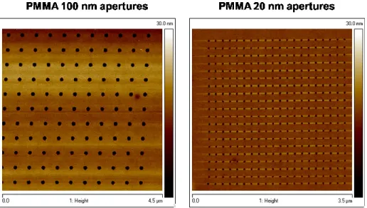
Figure 11 Optical image of the device we have fabricated in this thesis. The large GST square areas (l=100m) work as pad for the electrical access to a shrunk line region (w=25nm, L=410nm, th=20nm), in the inset, that is the active memory part of the device. Over it, Hydrogen silsesquioxane (HSQ) is deposited for passivation.
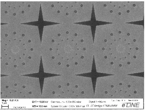
Starting from a line layouts, previously reported in literature [46], we scaled the active region sizes, simplifying the steps required to process the device. In Figure 11 an optical image of the device is shown. The large GST square areas (l=100m) work as pad for the electrical access to a shrunk line region (w=25nm, L=410nm, th=20nm). The inset of the figure shows a Scanning Electron Microscope (SEM) micrograph of this line region that is the active memory part of the device. Over it, Hydrogen silsesquioxane (HSQ) is deposited for passivation.
By suitable voltage pulses, 300ns long delivered by an HP81110A pulse generator, memory cell has been programmed. Also we have measured current and power during the pulse and we correlate them with the resistance of the cell, read in DC by a semiconductor analyzer.
The obtained well scalable structure is particularly suitable to study fundamental physics phenomena involved in the device working such as threshold switching, transitions, electromigration and doping. Electrical
Motivations
26
measurements on this test structures has been performed by Andrea Cattaneo at Politecnico di Milano.
27
Chapter 1
1
Nucleation and grain growth in as deposited and
ion implanted GeTe thin films
The working principles of PCM-based devices strictly depend on the amorphous characteristics. However, in a glass material, an infinite variety of amorphous states take place, depending on quenching and on deposition.
In this chapter we have studied the crystallization dynamic of GeTe 50nm thick films, deposited on a SiO2/Si substrate by RF magnetron sputtering, in
its three different amorphous states: as deposited, ion implanted and melt-quenched.
Since ion implantation represents a powerful tool to create amorphous regions in a controlled and reproducible way, in the first part of the chapter we present an insight of this technique for blanket films.
In the second part, we present our results obtained by means of in situ time resolved reflectivity measurements (TRR) and optical microscopy during annealing in the 143-155°C temperatures range on as deposited and ion implanted amorphous samples. The data are compared using the Johnson Mehl Avrami Kolmogorov (JMAK) model.
Finally, a more comprehensive explanation of the kinetic results is presented by means of Raman Spectroscopy on the as deposited, ion implanted and melt-quenched amorphous samples.
Chapter 1 - Nucleation and grain growth in as deposited and ion implanted
GeTe thin films
28
1.1 Ion Implantation in chalcogenide thin film
Amorphous phase in chalcogenide represents the crucial state of a device: this is essentially correlated to the RESET information stability, i.e. the propensity of amorphous phase to maintain its metastable arrangement upon increasing the temperature. Although stability enhances the data retention properties of devices, however, generally it elongates the pulse duration required to the SET (crystalline) programming [47].
A powerful tool to control the amorphization level of a specimen is ion implantation. This method consist of bombardment with ion projectiles that hitting the target can displace its atoms if the transferred kinetic energy is greater that the bounding energy. At each ion an amount of damage, i.e. target atom displacements, is then associated. When the damage reaches a threshold value amorphization occurs. The total distance which an ion mass travels in coming to rest in a target of atomic mass is called its range . The distance along the axis of incidence is called the projected range , and the distance travelled along the axis perpendicular to the axis of incidence is called the perpendicular distance . and are mean values because the number of collisions per unit path length and the energy lost per collision are random variables, i.e. all the ions having the same incident energy do not stop at the same location. There is instead a distribution in space of stopping points which is described by a range distribution function. The fluctuation or straggle in the projected range is . The perpendicular distance or the lateral spreading, , caused by multiple collision of the ions will increase with depth into the target and it is a function of the mass ratio . For , in th so-called heavy-ion implantation regime, we find and . For , a good lateral spreading estimation is while if , i.e. for light ions. In the classical scattering theory [48] the interaction between the moving ions with the
Ion Implantation in chalcogenide thin film
29
target atoms is described assuming two separate processes: elastic collisions with the nuclei, the so-called nuclear contribution, and inelastic collisions with the electron in the target, the so-called electronic contribution. The energy loss along the incidence direction x, is then described as | | (1.1)
The nuclear contribution is due to the Coulomb repulsion between the ion and the target nuclei. Excitation and ionization of host electron only affect the energy of the ion and they does not change its trajectory. In sum, every nuclear scattering event can deflect the ion trajectory while electronic energy loss only contributes to a continuous slowing down acting as a sort of friction force.
Generally, the nuclear term dominates at very low ion velocities while at higher ion energies electronic term can be several order of magnitude greater than the nuclear stopping. The occurrence of the first or the second regime, generally, depends on the comparison between the ion velocities and the velocities of the outer electrons of the host atoms.
When an ion impinges into the target it can displace host atoms from the crystalline lattice if the energy ceased by the ion is greater than the displacement threshold energy ( in Si and Ge, in Sb and Te). The extra energy acquired by the knock-on atom, , can be spent to travel through the target itself and produce secondary collisions, hitting other atoms, giving them energy and eventually producing secondary knock-on atoms if the energy is enough, and so on in a process called collision cascade. Displacing atoms from their lattice position collision cascades produce defects (interstitials, vacancies, etc.) in the target material.
Figure 12 and Figure 13 show collision cascades along beam incidence and transversal directions, respectively. Primary ion trajectory is shown in red,
Chapter 1 - Nucleation and grain growth in as deposited and ion implanted
GeTe thin films
30
while secondary cascades are represented in green. The damage is then localized where the cascades overlap.
Figure 12 Ge+ ions at 40 keV, impinging on a GST sample, produce collision cascade, shown along the beam incidence direction. Ion trajectories are indicated by red dots while secondary knocked out atoms in green.
Similarly to the ion range, we can associate several parameters to the damage profile. Approximating this profile with a Gaussian distribution we identify its center along the axis of beam incidence with and we indicate with the relative straggling. The damage distribution extends also in the perpendicular direction and we indicate the relative lateral straggling as .
The damage distribution is mainly related to the energy deposited in nuclear encounters. This last term is related only to the ion energies and to the masses of the projectile and of the target atoms. The distribution of this energy can be deduced either analytically or based on Monte Carlo
procedures. Nuclear encounters require target atoms and ions to approach very close, therefore, the probability for three or more particles collisions is extremely small.
Ion Implantation in chalcogenide thin film
31
Figure 13 Ge+ ions at 40keV, impinging on a GST sample, produce collision cascade, shown along the transversal direction (with respect to the beam incidence axis). Ion trajectories are indicated by red dots while secondary knocked out atoms in green.
Both simulations and calculations are then based on the Binary Collision Approximation (BCA). By the SRIM code [49], for instance, it is possible to simulate the ion implantation process with results closer to the experimental ones. The final structure of the damage depends however on the material, semiconductor, metal, insulator, etc., and on the temperature. In a semiconductor, for instance, light ion collisions occurs at a mean free distance very large with respect to the lattice parameter. As a consequence, damage is represented by a diluted distribution of point defects and the displaced atom profile present a buried peak. On the contrary, heavy ions the collision mean free path is of about the interatomic distance and, therefore, dense collision cascades are generated. Recoiled atoms transfer energy and damage to greater depths, producing the main contribution to the final damage profile.
Chapter 1 - Nucleation and grain growth in as deposited and ion implanted
GeTe thin films
32
Figure 14 Ge+ range distribution (Ions) and Ge, Sb, Te recoils, referred to the dose, along the beam incidence direction (SRIM calculation). Ion energy was set to 40 keV.
The elastic recoil loss, , is always 20%-30% less than the total nuclear stopping power because a fraction of the kinetic energy ceased to the target atoms is released by electronic excitations in subsequent collisions. The number of the displacement density can be obtained from using the modified Kinchin and Pease expression:
(1.2)
From the last expression, the target density (at/cm3) and the ion dose (at/cm2) we can calculate the number of Displacements Per (target) Atom (DPA):
(1.3)
As a rule of thumb, generally amorphization occurs when , i.e. when there is a displacement in the target lattice every three atoms. As shown in Equ. (1.3), the ion dose plays a relevant role in reaching the amorphization threshold. Heavy ions produces large collision cascade, in which each particle can displace about target atoms, with a
Ion Implantation in chalcogenide thin film
33
damage lateral straggling of the order of ten nanometers. For low fluences ( ) this produces isolated damage regions around each ion track. Complete cascade overlap requires high fluence ( ) producing an uniform lateral distribution of damage and, therefore, amorphization. In Figure 15a we show the DPA as function of the longitudinal direction, of a 20nm GST thin film on SiO2, covered by 10nm of amorphous Silicon and the
line of amorphization threshold (red).
Figure 15 (a) DPA produced by 1014 Ge+ ions/cm2 at 40 keV on a 20nm GST film protected by 10nm of amorphous Silicon. (b) Threshold amorphization fluence produced by different ions and energy at R.T. (squares) and at LN2 temperature.
Finally, temperature plays a relevant role in determining the effective amorphization fluence. Electronic energy (and extra displacement energy ceased to host atom during nuclear encounters) is dissipated by lattice vibration. As the temperature increases, defect mobility increases exponentially and, as a consequence, they can partially annihilate dynamically the produced damage. This observation justify the experimental results (Figure 15b), performed on a GST thin film [50], showing that the amorphization threshold depends on the temperature of the target during the implantation: it decreases as the target temperature decreases.
Chapter 1 - Nucleation and grain growth in as deposited and ion implanted
GeTe thin films
34
1.2 Comparison between as deposited and ion
implanted amorphous GeTe by Optical
Microscope
In the first part of this study, we have irradiated amorphous regions next to as deposited ones on a GeTe thin film using the masking technique aforementioned. Thin GeTe films 50 nm thick were deposited at room temperature (RT) by RF-magnetron sputtering, from a stoichiometric target, over a thermal 550 nm thick SiO2 covering a Si substrate. Then, each sample
was covered with a gold circular mask (thickness ≈ 25 m, diameter ≈ 3 mm).
The ion irradiation was performed at R.T. using 130 keV Ge+ ions at fluence of 1x10¹⁴ ions/cm2. This dose and the beam energy values were chosen in such a way to reduce the effect of sputtering, produced by Ge+ ions at high fluencies (>1x10¹⁵) and then to avoid any appreciable change in the stoichiometry of the film.
The ion projected range Rp (obtained through SRIM simulations) is 54 nm,
with a straggling Rp ≈24 nm (Figure 16).
Comparison between as deposited and ion implanted amorphous GeTe by Optical Microscope
35
The beam current was kept constant to smaller values (100 nA) to avoid heating of the sample. A nearly uniform nuclear energy loss across the layer thickness was also obtained with the settled irradiation parameters Figure 17.
Figure 17 Energy to recoils produced by ion implantation of Ge+ ions at 130 keV
As one can note from Figure 18, displaying the DPA, this configuration produces a good distribution of damage along the sample, well over the 0.3 amorphization threshold.
Chapter 1 - Nucleation and grain growth in as deposited and ion implanted
GeTe thin films
36
Figure 18 DPA produced in a 50 nm thick GeTe film by 1014 Ge+ ions/cm2 at 130 keV
Once we have two kinds of amorphous GeTe in the same specimen, the crystallization kinetic of the sample has been investigated in situ by means of Optical Microscopy during annealing in the 143-155 °C temperature range. The Mitutoyo microscope used during the observation was equipped with a 20x objective lens and a stage position measurement system. With this configuration, the images of the sample were stored with an optical resolution ≈1 m. During the annealing processes, oxidation was avoided by continuously fluxing the sample with dry nitrogen.
The large area covered by a single GeTe grain, few microns, before coalescence permits a direct estimation of the nucleation and growth processes.
Comparison between as deposited and ion implanted amorphous GeTe by Optical Microscope
37
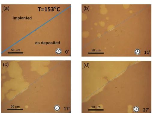
Figure 19 Optical sequence of a GeTe sample irradiated with Ge+ at a fluence of 1x10¹⁴ ions/cm2 on the left upper region (a) and annealed at 153 °C. The crystallization dynamic is faster in the implanted region where it is complete after 27 minutes (d) while in the contiguous unirradiated amorphous region the process is just starting. Note that the grain growth velocity slows down at the border of the unirradiated area (dashed line).
A typical sequence of optical images is shown in Figure 19 for a sample annealed at 153 °C. The analyzed region spans both an as deposited amorphous area and a contiguous irradiated amorphous region. The sample was annealed at 153 °C for different times. The enhancement of both nucleation rate and grain growth velocity in the irradiated area is clearly visible as well as the stop of the growing grain at the border of the unirradiated area. In addition, the sharp interface between the ion implanted and as deposited amorphous regions permits a direct observation of the change in the growth velocity of a grain when it crosses the boundary of the two systems.
Chapter 1 - Nucleation and grain growth in as deposited and ion implanted
GeTe thin films
38
At each settled temperature several images have been stored. From them, the area of each grain has been obtained and the relative radii have been calculated by circle-area approximation, i.e. valuating the area of each grain and assigning to it a radius measurement √ .
In Figure 20 the radius of the crystalline grains measured in the as deposited and ion implanted regions is reported as a function of time during annealing at 149 °C. The data refer to the size of five different grains in each region. The grain radius increases linearly with time and the slope (extracted from the linear fit) directly gives the growth velocity. The growth velocity, at 149 °C, in the as deposited amorphous region is G=2.7± 0.1 nm/s, rising to G=9.3± 0.5 nm/s in the irradiated area. Similar experiments were performed at other temperatures, and all over the investigated range the growth of the grains in the irradiated region is nearly three times faster that measured in the un-irradiated area.
Figure 20 Time dependence of the grain radius during annealing at a temperature of 149°C in irradiated and unirradiated amorphous regions respectively. For each set of data, the line (solid for the as deposited samples and dashed for the implanted ones) represents the linear fit of the radius as function of time (correlation coefficients > 0.99). The growth
Comparison between as deposited and ion implanted amorphous GeTe by Optical Microscope
39
velocity, G=9.3±0.5 nm/s (defined as the slope of the linear fit), is 3 times faster in the region implanted with 1014 ions/cm2.
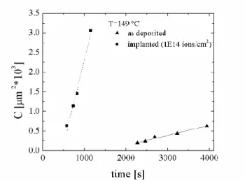
The grains surface density has been measured as a function of the annealing duration. As an example, the time dependence of the grain density during annealing at 149 °C is reported in Figure 21. The slope of the curve gives a measure of the steady state nucleation rate and an enhancement of the nucleation rate in the irradiated area by a factor ≈13 is clearly visible.
Figure 21 Time dependence of the grain density C, at the annealing temperature of 149 °C in the irradiated (1x10¹⁴ ions/cm2) and unirradiated regions. For each set of data, the line (solid for the as deposited samples and dashed for the implanted ones) represents the linear fit of C as function of time (correlation coefficients > 0.99).
The grain growth velocity has been reported in Figure 22 in a semilog scale as a function of 1/kBT for both irradiated and un-irradiated regions. The
reported values are the averages performed on several grains and the error bar indicates the spread of the measurements. A similar procedure was adopted for the temperature dependence of the nucleation rate and the data are reported in Figure 23.
Chapter 1 - Nucleation and grain growth in as deposited and ion implanted
GeTe thin films
40
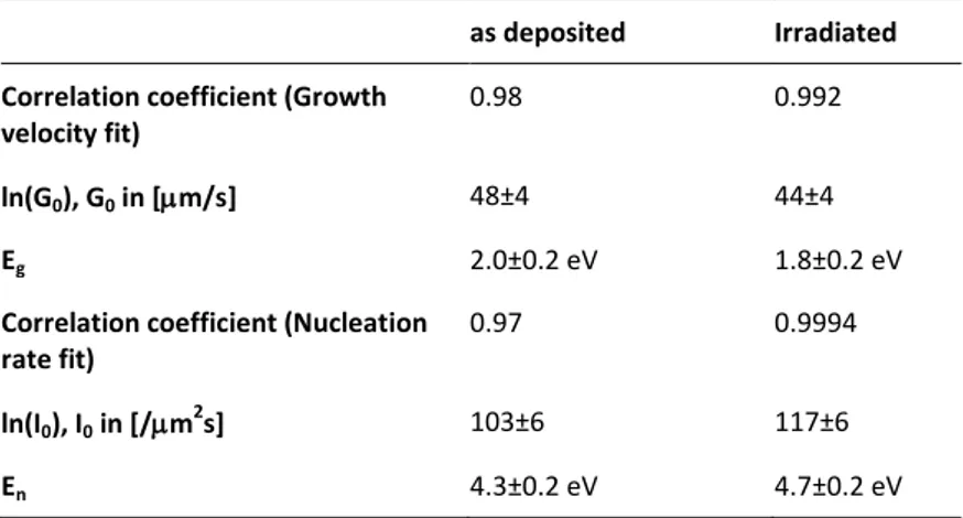
Figure 22 Arrhenius plot of the grain growth velocity, G, at several temperatures for the as deposited amorphous (▲) and the implanted (■) samples respectively. For each set of data, the line (solid for the as deposited samples and dashed for the implanted ones) represents the linear fit of ln(G) as function of 1/kBT. The fit parameters, G0 and Eg according to Eq. (1.4), and the correlation coefficients are reported in Table 1.
Both the graphs show that grain growth velocity and nucleation rate follow an Arrhenius behavior, respectively given by
(1.4)
and
I=𝐼 /( 𝐵T)} (1.5)
being and 𝐼 the pre-exponential terms and and the activation energies of the two processes respectively. The value of and have been extracted by the linear fit of data as function of . The same procedure was used to extract the value and 𝐼 from the nucleation data. The fitting parameters and the correlation coefficients of these fits are reported in Table 1.
Comparison between as deposited and ion implanted amorphous GeTe by Optical Microscope
41
Figure 23 Arrhenius plot of the nucleation rate, I, at several temperatures for the as deposited (▲) and the implanted (■) samples respectively. For each set of data, the line (solid for the as deposited samples and dashed for the implanted ones) represents the linear fit of ln(I) as function of 1/kBT. The fit parameters, I0 and En according to Eq. (1.5), and the correlation coefficients are reported in Table 1.
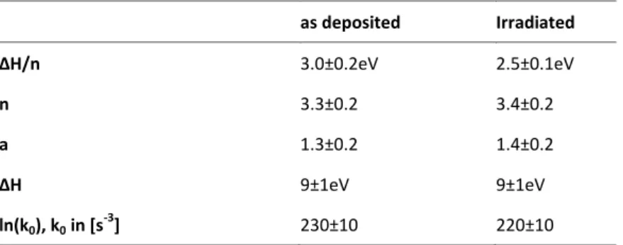
Table 1 Crystallization parameters of GeTe as found by in situ optical measurements.
as deposited Irradiated Correlation coefficient (Growth
velocity fit)
0.98 0.992
ln(G0), G0 in [m/s] 48±4 44±4
Eg 2.0±0.2 eV 1.8±0.2 eV
Correlation coefficient (Nucleation rate fit)
0.97 0.9994
ln(I0), I0 in [/m2s] 103±6 117±6
Chapter 1 - Nucleation and grain growth in as deposited and ion implanted
GeTe thin films
42
1.3 Comparison between as deposited and ion
implanted amorphous GeTe by TRR
measurements.
Figure 24 Time Resolved Reflectivity setup. The sample is placed in a vacuum chamber at a pressure of about 10-3 Torr. Samples is heated at a set temperature with a PID controlled heater. During annealing, a 5mW He-Ne laser beam reflects on the sample and its power is then measured by a photodiode.
Time resolved reflectivity measurements, using a He-Ne laser (λ=633 nm, P=5mW), were performed to monitor the fraction of crystallized material during the annealing in the range 147-154 °C. The sample were placed in a vacuum chamber at a pressure of about 10-3 Torr (Figure 24). For both the systems, the heating rate was 10° C/min and the settled temperature was constant within ± 0.1 °C.
This method takes advantage of the difference between the optical constants of the two phases to correlate the actual reflectivity to the fraction of transformed material over the probed region that is of the order
Comparison between as deposited and ion implanted amorphous GeTe by TRR measurements.
43
of the laser extinction length (10 and 20 nm for crystal and amorphous GeTe, respectively). However, the crystallized film has a columnar structure with a crystalline grain size of the order of few microns and so it’s reasonable to assume that the volume fraction of crystalline material coincides with the surface fraction detected by TRR.
Typical time resolved reflectivity curves of unimplanted amorphous GeTe, annealed at different temperatures, are shown in Figure 25. The crystalline volume fraction χ is obtained from the experimental TRR data, according to the linear approximation, widely demonstrated for GST [51]:
(1.6)
Where is the crystalline fraction on the probed sample, is the measured reflectivity, is the reflectivity of an amorphous sample and is the reflectivity of a crystalline sample. This equation assumes that
the grains have a prism-like-shape across all the film thickness with a base at the free surface and it has been extensively adopted in literature to study the crystallization of chalcogenide amorphous layers.
Figure 25 Time dependence of the reflectivity during annealing at different annealing temperatures of as deposited amorphous GeTe layers.
Chapter 1 - Nucleation and grain growth in as deposited and ion implanted
GeTe thin films
44
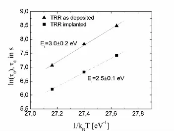
We define the characteristic crystallization time as the time at which the
time-derivative of χ(t) reaches the maximum, being the origin of the time scale coincident with the time at which the settled temperature is reached. The characteristic time of the as-deposited and implanted samples is reported in Figure 26 as a function of the inverse of temperature. An enhancement of the crystallization rate occurs in irradiated GeTe over the investigated temperature range. The 0 values measured at different
temperatures follow an Arrhenius law with an activation energy of Ei=3.0±0.1 eV and Ei=2.5±0.1 eV for the unimplanted and implanted
samples, respectively.
Figure 26 Arrhenius plot of the crystallization time, 0, at several annealing temperatures for the as deposited (square) and implanted amorphous (triangle) samples.
The JMAK Model
45
1.4 The JMAK Model
The information achieved by TRR is global, since it does not discriminate the different contributions responsible of the crystallization, i.e. nucleation and growth of the new phase. On the other hand, the nucleation and growth terms have been independently determined by means of optical microscopy.
In this context a reliable model is necessary in order to connect the two different approaches and to analyze them in a wider context. The JMAK model [52-59] connects the transformed volume fraction, during isothermal annealing, to the nucleation and growth parameters. This model assumes a random nucleation in the amorphous layer and neglects the lag time, before which the nucleation rate is zero. At a given temperature T, the time dependence of the crystalline volume fraction χ is given by
(1.7)
where the Avrami exponent n is an integer that depends on the nucleation and growth mode, and is a parameter whose temperature dependence follows an Arrhenius law:
(1.8)
where H is the activation energy of the whole crystallization process. It has been shown [60] that the Avrami exponent is given by:
(1.9)
where a is the nucleation index, b is the dimensionality of the growth (b=1,2 or 3, one, two or three-dimensional growth of the crystalline grain) and c is the growth index. In the present case b=2 and c=1, being the growth two dimensional and interface-controlled. In fact, the grain size is much larger than the film thickness and the growth velocity is time independent all over
Chapter 1 - Nucleation and grain growth in as deposited and ion implanted
GeTe thin films
46
the investigated range (Figure 20). The nucleation index a is correlated to the time dependence of the nucleation rate I by the following
𝐼 𝐼 (1.10)
where En is the activation energy for nucleation. In our sample a=1 since we
have shown (Figure 21) that the grain density increases quite linearly with time. Therefore in the investigated regime both the nucleation and growth rate are time independent and then Eqs. (1.4) and (1.5) well describe the temperature dependence according to the JMAK model. Under these conditions the k parameter is related to the nucleation and growth rate according to the relation
𝐼 (1.11)
Moreover, the overall activation energy for crystallization H is related to the activation energies of the individual processes, En and Eg, by the
following:
H=En+bcEg (1.12)
In our analysis En and Eg were determined by in situ optical microscopy; H
was estimated from TRR measurements.
In the JMAK model approximation, crystallization , described with Eqs. (1.4)(1.5)(1.6), take places after an incubation time, during which no nucleation and growth processes occur. Incubation time is temperature-dependent according to the equation
0=00exp{+Ei/(kBT)} (1.13)
where Ei is an activation energy related to the JMAK parameters according
to the equation
![Figure 10 [42] Schematic of the carrier injection mechanism responsible for the threshold switching in chalcogenide](https://thumb-eu.123doks.com/thumbv2/123dokorg/4479455.32281/30.892.188.706.104.318/figure-schematic-injection-mechanism-responsible-threshold-switching-chalcogenide.webp)