This Master thesis was accomplished within the Erasmus Mundus Joint Master Degree “Photonic Integrated Circuits, Sensors, and NETworks (PIXNET).”
Coordinating Institution: Scuola Superiore di Studi Universitari e di Perfezionamento Sant'anna Partners
Osaka University Aston University
Technische Universiteit Eindhoven
Project Data
Start: 01-09-2017 - End: 31-08-2022
Project Reference: 586665-EPP-1-2017-1-IT-EPPKA1-JMD-MOB EU Grant: 3.334.000 EUR
Website: http://pixnet.santannapisa.it
Program: Erasmus+
Key Action: Learning Mobility of Individuals Action Type: Erasmus Mundus Joint Master Degrees
Abstract
Spot size converters have a crucial role in integrated optics. This project is aimed to characterize and propose a new design of the spot size converters. An experimental assessment of a set of spot-size converters, where the coupling loss, polarization-dependent loss, and the transmission characteristics were analyzed, is performed, and a coupling loss as low as 1 dB was obtained. Motivated by the experimental results as an initial guess, two modeling approaches are proposed: (a) when the fiber matched waveguide is defined by thick lightly doped InP layer and highly doped InP substrate, (b) when the fiber matched waveguide is defined by diluted InGaAsP/InP interleaved layers. The study and optimization of respective parameters were performed, and the second approach relatively gives better coupling with a coupling loss of 0.4 dB with a taper length of 2.2 µm.
I. INTRODUCTION
owadays, many of the components required to deploy current and future complex optical communication networks have reached an appreciable state of maturity with the help of photonic integrated circuits. Impressive data performance is obtained by a variety of optoelectronic semiconductor devices such as lasers, amplifiers, switches, and modulators. Similarly, the transmission capacity of glass optical fiber is exponentially approaching the theoretical limit allowing the coverage of the universe. The full exploitation of these interesting achievements is, however, hindered by a limitation in delivering the data from the optoelectronic devices to the fiber and vice versa. A significant amount of power is lost at the interface, which is a bottleneck for the efficient communication of the data.
As a result, one of the key requirements of constructing communication networks using optoelectronic components is an efficient coupling between single-mode fibers and waveguides. A significant coupling loss is caused by a spot size mismatch between an integrated optical semiconductor waveguide and a single-mode fiber. The very small refractive index contrast in a glass fiber (Δn<5*10 ) results in a weakly guided optical N
yields a mode which is approximately lower than 2 µm[1], [2]. Besides, the mode shapes are circular in optical fibers but elliptical in waveguides. The ellipticity shape is due to the asymmetric dimensions of the waveguide. The variation in mode profiles will cause a mismatch during coupling. Thus, the coupling loss between an integrated optoelectronic device and an optical fiber takes an invaluable part of the power budget. Calculations give the coupling loss from InP waveguide to a standard single-mode fiber in the order of 10 dB.
Several approaches[1], such as the use of microlenses, lensed, or tapered fibers, improve the coupling efficiency[3], [4]. These fibers have a component that converts the standard fiber mode to a mode with a smaller size at the tip of the fiber. This reduction in fiber mode is achieved by either tapering down the core of the standard fiber or using microlenses at the tip of the fiber, or by deploying a combination of both. There exist commercially available lensed or tapered fibers that have mode field diameter as low as 2 µm that match to photonic integrated circuit waveguides. However, there is one disadvantage to this approach, where reducing the mode field diameter at the fiber tip to match to that of the waveguide results in critical requirement in alignment tolerance[5].
The Accuracy with which the fiber should be aligned to the waveguide is expressed by a parameter called 1-dB alignment tolerance. 1-dB alignment tolerance is the amount of displacement between the waveguide and the fiber mode, which leads to a 1-dB reduction in mode mismatch loss from its maximum matching
value. The majorityof these techniques reduce the size of the fiber mode, but the shape remains unchanged.
Lensed fibers can be designed in a way that could alter both the size and the shape of the mode profile[6]. With lensed fiber, coupling loss towards the waveguide is found to be in the order of 3-4 dB using overlap integral calculations. The decrement in fiber diameter, hence resulting in the reduction of fiber mode field diameter, causes low alignment tolerance.
Thus, to simultaneously decrease the coupling loss and maintain high alignment tolerance, both waveguide mode and fiber mode should be large enough. This can be achieved by increasing the spot size of the
integrated waveguide; hence, drives the need for SSCs. Since SSCs are promising solutions for mode transformation from a narrow waveguide to optical fibers, investigation of their performance is crucial.
Spot size converters are devices that transform the small on-chip mode in semiconductor waveguides to a field profile that resembles the fiber mode without affecting the alignment tolerances. An overview of different SSC structures has been given by Moeman et al.[1]. SSCs are generally categorized into two categories: Laterally tapered SSCs and vertically tapered SSC.
In the lateral tapering approach, the width of the waveguide is gradually tapered down to a cut-off width, upon which the field will be no more confined by it. Thus, the field will smoothly be coupled from the integrated photonic waveguide to adjacent waveguide, which is fiber matched waveguide. The tapering should be done gradually so that the mode is converted adiabatically, and no optical power is radiated away from the fundamental mode. Lateral tapering, reported in[7]–[14], is a simple and easiest approach. The difficulty in lateral tapering is the realization and control of the narrow, sub-micron levels, tip width.
In vertical tapering, the thickness of the primary guiding layer is slowly tapered down until it reaches cut-off. In this type of taper, an optical mode is adiabatically coupled from the tapered down layer to the next higher refractive index layer. In a material composed of different layers, the optical mode is confined in a layer with the highest refractive index. Once this layer reaches cut-off, the mode goes to the layer with the next higher refractive index, which is optimized to match to a fiber. Since most of the fabrication process are planar, vertical tapers are challenging to realize.
SSCs with a combination of both categories [15]–[17] are widely deployed to get their respective advantages. In this project, vertically separated InP-based waveguides[18], [19], where the upper waveguide is laterally tapered, are used.
The main objective of this project was to assess the performance of a spot size converter and to come up with solutions that can improve the performance. A set of spot size converters was fabricated via a generic InP integration process from an established foundry. The experimental assessment was performed to identify which SSC performs the best. But the main challenge of the project was, we do not get the design information
results, a guess of the design was made, and a new design was suggested. The organization of the report after this is as follows. Section II explains the concepts of the spot size converter. Section III discusses experimental procedures followed and the results obtained. In section IV, new approaches for designing the SSC are proposed. Then, simulation results are discussed in section V. Finally; the report is winded up with a conclusion in section VI.
II. CONCEPTSOFTHESPOTSIZECONVERTER
A tightly confining conventional waveguide is necessary for connecting different components of the photonic integrated circuit, while a loosely confining large waveguide is necessary for efficient fiber coupling. To simultaneously achieve both the functions, two waveguides of different dimensions are used— the difference in dimension results in a difference in propagation constant. A mode that is guided in one of the waveguides will not be guided in the other. Tapering down the tightly confining waveguide will enable us to smoothly couple the mode to the loosely confining waveguide.
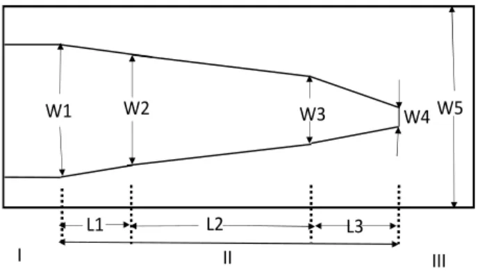
As shown in Figure 1, the spot size converter contains three regions: (I) conventional waveguide region, (II) tapered region, and (III) a large mode size fiber matched region. The structure of the region (I) is the same as that of conventional semiconductor (InGaAsP/InP) waveguides[20], [21]. It has a width, W1, 1.5 μm, and thickness, t, 0.5 μm.
Region (II) is the spot size conversion region, which in turn contains three sub-sections, (L1), (L2) and (L3). Each sub-section is varied according to its width and length. The first sub-section (L1) is used to change the width of the input waveguide to a width where coupling starts. The longest sub-section, (L2), plays a crucial role in transferring the mode profile. The variation in width has to be very slowly such that the fundamental mode in each consecutive cross-section overlaps effectively without radiating to higher-order
Figure 1: Top view of spot size converter
Region (III) is the fiber matched InP waveguide region, which has a comparable dimension to lensed single-mode fiber. This waveguide is optimized such that it will be able to couple the light to both the single-single-mode fiber and the standard waveguide.
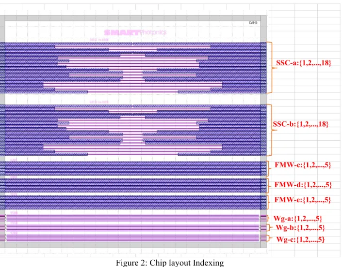
The characterized photonic chip, presented in Figure 2, contains three sets, each containing two or three replicas of the same structure by varying some parameters. The first set, SSC a and SSC b, includes two 18 waveguide groups with varying spot size converter (SSC) length and width. These spot size converters contain three sub-sections, as depicted in the region (II) of Figure 1, on which the length and width of each sub-section are varied to observe the coupling loss.
Thus, a single SSC, for instance, SSC a1, is arranged as fiber matched waveguide, adiabatically tapered section, and conventional waveguide from fiber to an optoelectronic circuit. The second set contains three
W1 W2 W3 W4
L1 L2 L3
I III
W5
subsets (FMW-c, FMW-d, and FMW-e), each containing five elements. These sets have a uniform cross-section fiber matched waveguides, which will be used as a reference during characterization. Finally, the third set contains three subsets (Wg-a, Wg-b, and Wg-c). Each subset contains five conventional waveguides of different parameters, such as width.
III. EXPERIMENTAL PROCEDURES AND RESULTS
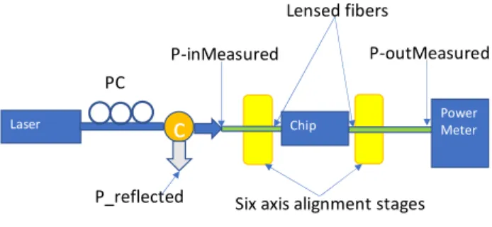
A testbed has been set up as shown in Figure.3, for experimental assessment of the chip. A tunable laser operating at C-band centered at 1550 nm is used as a source where its output is fed to the polarization controller (PC). The alignment was performed via two six-axis stages with two lensed fibers used to couple the light from the laser to the chip or from it to the optical power meter. A polarization controller has been connected to the lensed fiber at the input to optimize the polarization. A circulator has been then connected
Figure 2: Chip layout Indexing SSC-a:{1,2,3,…,18} SSC-b:{1,2,3,…,18} SSC-c:{12,…,5} SSC-d:{12,…,5} SSC-e:{12,…,5} Wg-a{1,2,…,5} Wg-b{1,2,…,5} Wg-c{1,2,…,5} SSC-a:{1,2,...,18} SSC-b:{1,2,...,18} FMW-c:{1,2,...,5} FMW-d:{1,2,...,5} FMW-e:{1,2,...,5} Wg-a:{1,2,...,5} Wg-b:{1,2,...,5} Wg-c:{1,2,...,5}
to measure the reflected power. For each element, the corresponding input power, reflected power, and output power (P-inMeasured, Preflected, and P-outMeasured) are measured at center wavelength. The laser and the power meter were connected to a computer through a general-purpose interface bus (GPIB) to perform wavelength scanning automatically and for automatic data acquisition. A MATLAB code was used to control the laser wavelength sweep.
Figure 3: Schematic of the experimental setup
To measure the coupling loss, we first measured the input and output powers of respective SSC or waveguide by aligning the input and output fibers. Since both ends of the waveguide are cleaved facets, they act as mirrors with certain reflectivity. The reflectivity is measured and fits with the assumptions used as in [22] of modified Fabry Perot interferometric loss measurement. The coupling loss is calculated using the equation:
Lc = End_to_End_loss − Lr − Lp − 1.19dB (1)
Where Lc is the coupling loss, End_to_End _loss is the total loss between the power measured at the input and output of the chip, Lr is the reflection loss, and Lp is the propagation loss due to linear absorption within waveguide of length L.
The constant 1.19 dB is the calibrated losses due to connectors used, fiber to fiber loss, and circulator's port 2 to 3 loss. The propagation loss, Lp, is found from the measured values using equation (2).
L = e (2)
Where
α[dB cm] = 4.34 ln √√ (3)
Laser
c
Chip PowerMeterP-outMeasured
Six axis alignment stages PC
P-inMeasured
Lensed fibers
Where α is the propagation loss coefficient, R is the reflectivity of both the input and output facets, r is the ratio of maximum and minimum output power taken from the output spectrum.
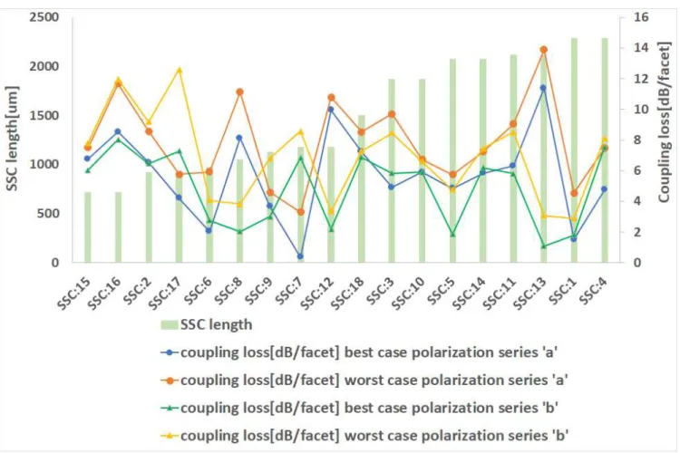
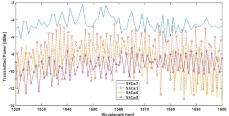
Figure 4 depicts the measured coupling losses of spot size converter series a and b. The SSCs are sorted out in increasing length using bar graphs, and the coupling losses are presented by the scatter points connected by lines. The SSCs have three sections upon which parameters such as length, width, and geometrical arrangements are varied to investigate the best performing SSC. Based on our measurement SSC:7 a, SSC 5
b, SSC:8 b, SSC 13 b, and SSC 1 a and b has coupling loss of less than 2 dB/facet. This is because their
second sub-section, W2 to W3 in Figure 1, of the taper experiences a small taper angle leading to a smooth change in consecutive cross-sections. The smooth transition will allow the mode to adiabatically couple to the FMW. The other sets which experience higher loss could be due to a short length of either the second or the third taper sections, which will cause an abrupt transition between adjacent cross-sections. This will result
in radiating the mode to cladding modes, and significant reflection between intermediate waveguide widths. Another observation that can be analyzed is the dependent loss. The SSCs are polarization-dependent. The polarization-dependent loss of the best performing sets is 5.8 dB, 3.6 dB, 4 dB, 6 dB, and 2.17 dB, respectively.
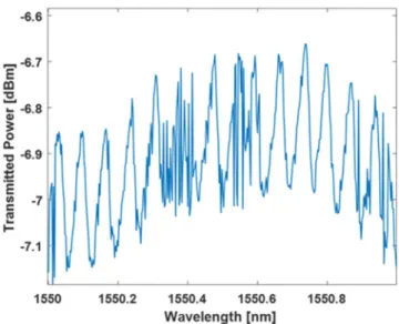
Taking the polarization giving maximum output power wavelength scanning is performed. Assuming that the input power remains constant, the ratio of maximum and minimum output intensity from the fringes of the Fabry Perot effect of the waveguide is calculated, which is used to calculate the total propagation loss per length within the respective waveguide. Figure 5 shows the transmission characteristics of waveguide a, which is used as a test reference. Subtracting this loss from the total input to output loss gives the coupling loss of the spot size converters.
The power transmission as a function of the wavelength for the best performing sets from both series exhibits similar properties. Figure 6 shows that the output power oscillates with respective maxima and minima because the facets act as a mirror and the waveguide as a resonating medium resulting in a quasi-sinusoidal pattern.
Figure 6: Transmission characteristics of best performing SSC "a" series
The oscillations are not purely sinusoidal, since the range of wavelength and number of steps is large. IV. DEVICE REDESIGN
Inspired by the results obtained from the characterization, modeling of the spot size converter with the help of FIMMPROP is performed. The design of input waveguide, fiber matched waveguide, and finally, the whole spot size converter is performed step by step. The fiber matched waveguide design was achieved through two approaches A) Using lightly doped InP layer grown on highly doped InP substrate, and B) Using diluted structure formed by interleaving thin quaternary layer (InGaAsP) and InP layer. In the following, we investigate each of these points with their respective parameters to come up with a low loss device.
A. Input waveguide design
The input waveguide is standard deep etched single-mode InP/InGaAsP waveguide with width 1.5 µm and core thickness of 0.5 µm, as depicted in Figure 7. It has InP upper and lower cladding with a refractive index of 3.17 and 3.1676, respectively. The etching penetrates 150 nm to the lower cladding, also called a spacing layer that spatially separates the upper (input) and lower waveguides. This waveguide is optimized so that only the fundamental TE and TM modes are guided within the core of 0.5 µm InGaAsP, which has a refractive index of 3.36.
Figure 7: Input waveguide cross/section B. Fiber matched waveguide design
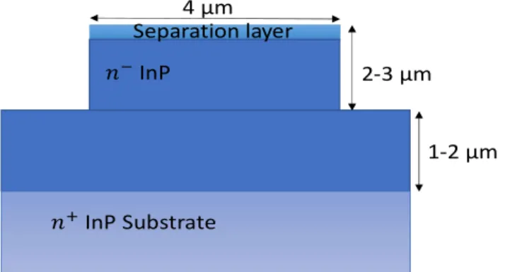
In this project, we propose two approaches for the design of fiber matched waveguide. In the first approach shown in Figure 8, the waveguide is defined by a lightly doped thick InP layer with respect to the highly doped InP substrate. This approach needs a thick fiber matched InP layer, which is a bit hard to grow. To come up with thicker InP layers, parameters such as gas flow rate and the temperature has to remain constant for a long-time duration. Also, the control of the relative doping concentration of the InP layer with respect to the substrate is a bit complex.
Figure 8: InP based fiber matched waveguide defined by doping concentration variation
The second approach, depicted in Figure 9, is where a diluted waveguide with alternative layers of thin quaternary and InP is used. Here the thickness is small, which will alleviate from thick layer requirement. The effective index of the waveguide is also made more closer to the upper waveguide, which facilitates the
𝑛− InP 𝑛 InP Substrate 0.5 µm 2µm 2 µm 1.35 µm 1.5 µm P-InP 2 µm 𝑛 InP 𝑛 InP Substrate 2-3 µm 1-2 µm Separation layer4 µm
Figure 9: InP/InGaAsP diluted structure-based fiber matched waveguide
Geometrically the fiber matched waveguide is designed to have a core of 4 µm by 4 µm by optimizing both the coupling efficiency to/from the fiber and the transfer efficiency to/from the conventional upper waveguide. In designing this waveguide, the number of modes supported should be considered carefully. Ideally, the waveguide should be single-mode by employing a small refractive index difference between the core and cladding materials needed, which may not be easy for realization. The single-mode operation can be achieved in two ways: by using small index contrast InP material introduced by varying the doping concentration[17],[23], and diluted structure with alternating InP and InGaAsP layers[15], [24].
In the doping induced mechanism, the waveguide can be made single-mode by using shallow mesa etch depth. The refractive index of the guiding and cladding layers has to be close to each other to realize single-mode operation; thus, the field confinement will be degraded. That is, a significant field will leak towards the substrate. Hence, it is not strictly needed for the fiber matched waveguide to be a single mode. Because the length of the fiber matched section is short, with reasonably proper fiber alignment, the fundamental mode will dominate even if some higher-order modes are supported. In case, some higher transverse and lateral modes are excited, the transverse modes are leaky and will quickly radiate to the substrate while the lateral will be filtered out by the upper waveguide.
In the diluted approach, the single-mode operation is easily obtained with the help of the 30 nm InGaAsP interleaved within InP spacings. As depicted in Figure 9, the red layers are InGaAsP with a refractive index of 3.36, and the layers enumerated by (1) are InP with a refractive index of 3.17. Layer (2) is an InP substrate
Q-Layer spacing 30 nm Q-layer Q-Layer position 1 1 1 1 2
with refractive index 3.155. The coupling from the upper standard single-mode waveguide to the diluted waveguide is optimized by varying the spacing between the quaternary layers. The respective thicknesses of the layers denoted by (1) from top to bottom are 1.01 µm, 0.86 µm, 0.69 µm, and 1.5 µm. A possible deviation of the spacings, quaternary layer thickness and composition may cause variation in coupling efficiency and has to be controlled carefully. Etching also needs to take into account the presence of the quaternary layers since they have different etching rate from InP.
C. Optimum spacer layer thickness
The upper waveguide and the underlying waveguide are separated by a thin InP spacer layer. Its function is to ensure that the field in the upper waveguide is well confined and spatially separated from the underlying fiber matched waveguide. In doing so, the layer reduces the coupling between the waveguides. Fixing the refractive index taken from the SMART photonics manual, the thickness upon which the maximum mode coupling occurs is optimized. The power transfer efficiency from lower to higher (and vice versa) waveguides has to be equally high. The spacer thickness upon which maximum transfer occurs is found by FIMMWAVE simulation, and its value is around 0.24 µm.
D. Design of the spot size converter
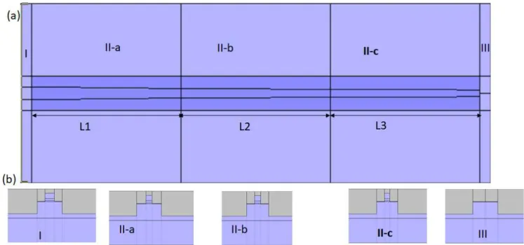
The design of the tapering structure is done based on light propagation investigation through the widely used propagation tool, FIMMPROP (PhotonDesign), for modeling and simulating optical waveguides. The main idea is to smoothly adopt the mode from the input down to the output cross-sections, guiding the light with very low losses and as short length as possible to come up with the required spot size. The structure is studied at a wavelength of 1.55 µm. As the fundamental TE and TM modes can still travel up to their respective cut-off width, we reduce the width to a point where the light will effectively couple to the fiber matched waveguide. Therefore, the spot size converter is composed of a series of cross-sections connected by a simple joint where the software calculates the coupling between consecutive sections. Figure 10 shows the top view of the spot size converters along with five consecutive cross-sections.
the measured structure. The spot size conversion region consists of three sub-sections (II-a, II-b, II-c), which facilitate the adiabatic criterion. Each section of the structure is therefore described as:
(I) Section (I) is the standard InP input waveguide with a width of 1.5 µm and a length set to 50 µm as in Figure 10 (b) cross-section (I)
(II-a) Section (II-a) is the first stage taper, which is defined by a length of 319.5 µm and width that linearly varies from 1.5 µm to 1.1 µm.
(II-b) Section (II-b) is the second stage of the taper, which is defined by a length of 1526.5 µm and width, which linearly varies from 1.1 µm to 0.94 µm. This is the region where the adiabatic criterion is supposed to be realized.
(II-c) Section (II-c) is the third stage of the taper that is defined by a length of 397.5 µm and a width that varies linearly from 0.94 to 0.6 µm. Its cross-section is depicted on Figure 10 (b) cross-section (II-c). (III) Finally, section (III) is the fiber matched waveguide that is defined by layers of the varying doping concentration of InP. It has a width of 4 µm, and its length is set to 50 µm. This waveguide is defined by etching away the standard InP waveguide, which was tapered down in the previous sections of the device.
The layer stacks of the devices are similar to those described in the input and FMW waveguide section of
this document. The fundamental TE mode is launched at the input of the standard InP waveguide. With the parameter set to the initial values, the propagation analysis was performed. Inspection of the scattering matrix of the device demonstrates that only 17% of the lunched TE0 is coupled to the TE0 of the fiber matched waveguide. The rest of the light is coupled to the higher-order modes; thus, the device does not couple the light effectively. This result motivates us to investigate various parameter variation effects. The parameters studied are the length of each section of the taper, the respective tip widths down the structure, and etch depth of the device.
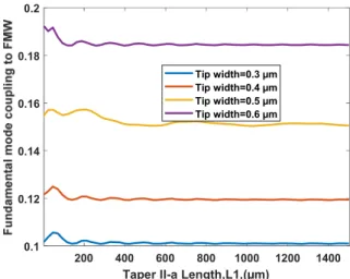
Let us begin by observing the coupling characteristics of the device when the FMW is designed using refractive index variation induced due to the doping concentration difference of InP. Fixing all the other parameters, L1 was scanned for different tip widths. As depicted in Figure 11, the coupling remains small and constant, even if the length increases for each tip width. Similarly, scanning of L2 behaves the same way as section L1, as can be seen from Figure 12. Fixing both L1 and L2 to the initial values, scanning of L3 is performed where the adiabatic mechanism takes place. Figure 13 shows, as the length, L3, increases the
Figure 10: (a) Top view of the spot size converter design, including the five cross sections (b) cross section at each stage
L1, and L2 scanning is the value when L3=319.5 µm (initial given value). With the given tip width, 0.6 µm, a significant coupling that is greater than or equal to 90% (0.45 dB loss) is obtained for a length, L3, greater than 5.4 mm. The length scanning results also imply that the light is confined in the upper waveguide until the tip width is decreased to about 0.8 µm, where the maximum coupling capability is observed. For a tip width of 0.9 µm, the coupling diminishes immediately, telling that the cut-off width for the standard waveguide is not reached. For tip widths lower than 0.8 µm, the coupling for a specific length decreases, implying that some percentage of light goes to radiation modes.
Observation of the coupling as a function of length enables us to deduce that tip width of 0.8 µm yields a maximum coupling at the shortest possible length. Choosing L1, L2, and L3 to 50 µm, 100 µm, and 1953 µm, respectively, the effect of etching depth is studied. Figure 14 shows the coupling behavior for three different etch depth values, 2 µm, 2.5 µm, and 3 µm. It implies that the coupling rarely depends on the etch value with etching 2 µm requiring a bit longer taper. To take advantage of the small improvements etch depth of 3 µm is used in for the design of the device
Figure 11: Coupling of TE0 as a function of section 1, L1, taper length for different tip width
200 400 600 800 1000 1200 1400
Taper II-a Length,L1,(µm)
0.1 0.12 0.14 0.16 0.18 0.2 Tip width=0.3 µm Tip width=0.4 µm Tip width=0.5 µm Tip width=0.6 µm
Figure 12: Coupling of TE0 as a function of section 2, L2, taper length for different tip width
Figure 13: Coupling of TE0 as a function of section 3, L3, taper length for different tip width
Figure 14: Coupling of TE0 as a function of section three taper length for different depths
F u n d a m en ta l T E m o d e C o u p li n g t o F M W F u n d a m en ta l m o d e C o u p li n g t o F M W F u n d a m en ta l m o d e C o u p li n g t o F M W
Similar to the previous approach, the effect of each section's length is discussed. Figure 15 shows the coupling dependence of the SSC on section two length, L2. For TM the coupling remains independent of the length and remains stable in the whole length range
Figure 15: Fundamental TE and TM coupling per section two length
For TE, the coupling first increases linearly and attains its stability, 99%, at about the length of 234 µm. The length has to be chosen around this value so that the coupling remains constant for some shifts. Length one also has a similar effect as section two length.
Figure 16 shows the coupling of the SSC as the function of the third taper subsection length variation. It clearly shows that the performance of the structure is determined by section three of the taper. Hence, both the first and second stages of the taper have the same role implying that we only need one of them. At a length of 2176 µm, both TE0 and TM0 modes have a coupling of 98% yielding zero polarization dependence. A length of 1250 µm can also be chosen to have a 95% coupling of TE0 and 76% TM0 with a polarization-dependent loss of 0.94 dB. F u n d a m en ta l m o d e C o u p li n g t o F M W
Figure 16: Fundamental modes coupling per section three-length E. Polarization dependence analysis
The polarization dependence[25], [26] of waveguide results from the geometrical birefringence due to the asymmetric shape of the waveguide as well as the difference in index contrast in the lateral and transverse direction. The change in the width of the waveguide causes a change in the effective index of the modes, which in turn results in a change in propagation constant. As the width varies, there is a point where both TE and TM modes intersect each other so-called critical width. At the critical width, both TE and TM modes have the same propagation constant; hence, the polarization-dependent loss is zero. Therefore, we need to find a tip width around which this effect happens.
Design of the initial, intermediate, and final widths of the upper waveguide (one which is tapered down) is an iterative process, starting from an initial guess to two of them while optimizing the third one for maximum coupling efficiency to the fiber matched waveguide. The intermediate widths which maximize the coupling efficiency are found to be W2=1.025 µm and W3=0.924 µm. Given the optimum value of all the other parameters, the power transfer as a function of the tip width for both designs is discussed in the consecutive paragraphs.
Figure 17 shows the coupling efficiency when the FMW is designed using thick 𝑛 − InP layer, which is grown over 𝑛 −InP substrate. For TE, the tip width at which the maximum power transfer, 99.01%, occurs is at about 0.825 µm. Beyond this width, the upper waveguide is wide enough to confine the mode, and no
F u n d a m en ta l m o d e C o u p li n g t o F M W
decreases, resulting in a leakage of light to modes which have lower propagation constant. This will accordingly cause decrement of the coupling to the fiber matched waveguide.
Figure 17: Coupling of fundamental modes as a function of section two taper length
Similarly, for the fundamental TM, the maximum power coupling, 96.1%, occurs at a tip width of 0.67 µm. If the width goes beyond this value, the field will tend to remain in the upper waveguide. As the width is further decreased, it results in radiating the field to higher-order leaky modes. The intersection width, 745 nm, is where both TE and TM modes have the same effective index; thus, the same propagation constant. This implies that the birefringence is close to zero, and our device is polarization insensitive. Both polarizations entertain a coupling efficiency of 91.3% from the upper waveguide to the fiber matched waveguide (and vice versa).
When the fiber matched waveguide is designed using diluted waveguide, the coupling from the upper waveguide to the lower waveguide is enhanced. The tip widths are optimized for optimum coupling efficiency towards the fiber matched waveguide. From Figure 18, the coupling efficiency is 94% at the tip width of 0.6 µm for both TE and TM mode polarization. This design is tolerant to fabrication errors with respect to the one designed using only InP layer. An increase of 50 nm in the tip width causes a coupling of 98% for TE and 91% for TM polarization. Similarly, a decrease of the same amount in the tip width decreases the coupling efficiency to about 87% for both polarizations.
F u n d a m en ta l m o d e C o u p li n g t o F M W
Moreover, at a tip width of 745 nm, this design yields 98% coupling for both TE and TM. It also gives relatively uniform coupling efficiency around its maximum value, letting it be more tolerant to fabrication errors compared to the lightly doped InP approach.
Figure 18: Coupling of fundamental modes as a function of upper waveguide width when the FMW is defined by a diluted structure
V. SIMULATION RESULTS
The field propagation down the structure for both approaches will be discussed in this section. In Figure 19, the intensity profile of the fundamental modes with 2D field profiles taken at different positions along the length of the structure is presented to show how the light is gradually coupled into the fiber matched
waveguide. Figure 19 (a) showed when the fiber matched waveguide is defined by index contrast created by
lightly doped InP layer grown over a highly doped InP substrate layer. At the input waveguide, both TE0, and TM0 are confined in the upper standard InP waveguide. At Z=900 µm, TM0 starts to transfer to the coupling waveguide, while the majority of TE0 is already coupled. When we check the position of the modes at Z=1600 µm majority of TM0 is coupled down to the fiber matched waveguide. But TE0 totally couples from the upper waveguide to the bottom waveguide. This is because for TE maximum power transfer occurs at a width which is very close to the Tip width; thus, it starts coupling faster than the TM0. The 2D field profile at the tip, a point where the upper waveguide ends, is pushed down to the bottom of the fiber matched waveguide for TE0, while there is still a small percentage at the upper waveguide for the TM0. Finally, at
According to the scattering matrix, 91.7 %, 0.4 dB loss, of the input light couples to the FMW for both TE and TM. For TE, 8% goes to the first order TE mode, while for TM, 8% of the light is still in the upper waveguide, since the tip width is higher than the cut-off width. The mode profile for both polarizations is a
(a)
(b)
Figure 19: (a) Field profile when the FMW is defined by InP doping concentration difference (b) field profile when the FMW is defined by diluted structure
bit elongated in the transverse direction and is asymmetric
The diluted approach can help us to change the center of the modes and enhance the symmetry of the profile. Figure 19 (b) shows the field propagation when the fiber matched waveguide is defined by Q-layers interleaved between InP layers. The fundamental TM mode remains confined in the upper waveguide until Z=1600 µm, where it starts to transfer towards the FMW. On the other hand, TE0 mode starts to couple effectively to the FMW at about Z= 900 µm, since the width at which both the waveguides have the same propagation constants occur fast with respect to the fundamental TM mode. At the tip, both modes are effectively coupled to the fiber matched waveguide; thus, no light is left in the upper waveguide, which is an advantage over the afro mentioned design.
Scattering matrix inspection shows us that 98%, 0.08 dB loss, of both fundamental TE and TM modes are effectively coupled to the FMW. Only 2% is radiated to the higher-order modes. Moreover, this design allows us to use a tip width of 0.6 µm with significant and polarization-independent coupling, which is more tolerant of the fabrication errors, as shown in Figure 18. The conversion loss at this tip width is only 0.3 dB.
Applying a butt-coupling technique, mode field diameter of a fiber, which gives a better coupling from the fiber matched waveguide, was analyzed. The mode dimension of the fiber matched waveguide is 3.8 µm * 4.5 µm, and that of the fiber is 3.6 µm * 3.6 µm. A coupling of 91% was obtained to a fiber with a mode field
diameter of 3.6 µm. The corresponding coupling loss is about 0.4 dB. The horizontal and vertical 1dB
alignment tolerances are 0.89 µm and 0.98 µm, respectively.
The wavelength dependence of TE and TM modes of SSC is shown in Figure 20. It can be seen that for TE mode, the SSC is broadband with a maximum loss of 0.31 dB (92% coupling) for a bandwidth of 40 nm. For TM mode, there is a higher loss at the lower wavelength end, approaching its cut-off. This could be improved by the compromise between the wavelength and width variations of the SSC. The total coupling
VI. CONCLUSION
In this project, a spot size converter was assessed for its performance by analyzing the power transmission and coupling loss properties. For the measured SSCs, the width variations with respect to the length of each stage of the taper play a crucial role in the coupling efficiency. Of the two proposed designs for the fiber matched waveguide, the diluted approach gives better coupling performance and more tolerant of waveguide tip width variation. Opting out the best performing SSC, modeling of new design yields an enhanced and polarization-independent coupling of 98.1 % to the FMW with a two-stage taper of length 50 µm and 2176 µm respectively. The first stage, whose width varies from 1.5 µm to 0.94 µm, is used to change the cross-section of the standard input waveguide to the cross-cross-section where coupling starts with low reflections. Similarly, the second section's width decreases adiabatically from 0.94 µm to .745 µm. A coupling loss of 0.4 dB is achieved to a fiber with a mode field diameter of 3.6 µm. Besides, the SSC is operational with the whole C-band.
In future studies, different geometries for the taper sections can be investigated to reduce the total length. Besides, the design of the fiber matched waveguide can be further engineered to get better performance and adapt to different fiber mode diameters.
Figure 20: The total taper coupling versus wavelength for the TE0 and TM0 s of the entire SSC
ACKNOWLEDGMENT
First of all, I wish to express my deepest gratitude to my supervisor, Dr. Nicola Calabretta, my co-supervisors, Kristif Prifti, and Dr. Simone Cardarelli, who supported me throughout the project. They have been consistently in touch with me and provided me with invaluable support and guidance whenever I needed it. Secondly, I would like to thank Dr. Netsanet Tessema, who was promptly responsive whenever I needed her help. I wish to thank all the people who assisted me in one or another way.
[1] I. Moerman, P. P. Van Daele, and P. M. Demeester, "A review on fabrication technologies for the monolithic integration of tapers with III-V semiconductor devices," IEEE J. Sel. Top. Quantum Electron., vol. 3, no. 6, pp. 1308–1320, 1997, doi: 10.1109/2944.658785. [2] I. Moerman et al., "III-V semiconductor waveguiding devices using adiabatic tapers," Microelectronics J., vol. 25, no. 8, pp. 675–690,
1994, doi: 10.1016/0026-2692(94)90133-3.
[3] H. M. Presby and C. A. Edwards, "Near 100% efficient fibre microlenses," Electron. Lett., vol. 28, no. 6, pp. 582–584, 1992, doi: 10.1049/el:19920367.
[4] N. Kalonji and J. Semo, "High efficiency, long working distance laser diode to single-mode fiber coupling arrangement," Electron. Lett., vol. 30, no. 11, pp. 892–894, 1994, doi: 10.1049/el:19940567.
[5] M. Dagenais, V. Vusirikala, S. A. Merritt, S. S. Saini, R. E. Bartolo, and D. Stone, "Alignment-tolerant lasers and silicon wafer board integration," Optoelectron. Interconnects Packag. IV, vol. 3005, no. April 1997, pp. 38–47, 1997, doi: 10.1117/12.271109.
[6] Y. He, S. K. Mondal, and F. G. Shi, "Design Optimization of Wedge-Shaped Lensed Fibers for Fiber-Laser Coupling: Fresnel Reflection and Non-Gaussian Mode Effects," J. Light. Technol., vol. 21, no. 10, pp. 2271–2275, 2003, doi: 10.1109/JLT.2003.818173.
[7] M. Osamu, K. Kazuo, and H. Miyazawa, "Design of a Single-Mode Tapered Waveguide for Low-Loss Chip-to-Fiber Coupling," IEEE J. Quantum Electron., vol. 30, no. 8, pp. 1787–1793, 1994.
[8] S. Demiguel et al., "Evanescently Coupled Photodiodes Integrating a Double-Stage Taper for 40-Gb / s Applications Compared Performance With Side-Illuminated Photodiodes," J. Light. Technol., vol. 20, no. 12, pp. 2004–2014, 2002.
[9] S. Ryu, S. Kim, J. Sim, J. Kim, and A. Member, "1 . 55 μm Spot-Size Converter Integrated Laser Diode With Conventional Buried-Heterostructure Laser Process," IEEE PHOTONICS Technol. Lett., vol. 15, no. 1, pp. 12–14, 2003.
[10] B. Mersali, H. J. Briickner, M. Fehllade, S. Sainson, A. Ougazzaden, and M. Carenco, "Theoretical and Experimental Studies of a Spot-Size Transformer with Integrated Waveguide for Polarization Insensitive Optical Amplifiers," J. Light. Technol., vol. 13, no. 9, pp. 1865–1872, 1995.
[11] M. Wada et al., "Fabrication and coupling-to-fiber characteristics of laser diodes integrated with a spot-size converter having a lateral taper," IEE Proceedings-Optoelectronics, vol. 144, no. 2, pp. 104–108, 1997.
[12] K. . Aniak, J. Kreiss, T. Hartwich, W. Rehbein, G. Wache, and H. Heidrich, “1.55 μm BH-DFB LASER WITH INTEGRATED SPOT SIZE CONVERTER FOR FLIP-CHIP APPLICATIONS,” 16th IPRM. 2004 Int. Conf. indium Phoshide Relat. Mater., pp. 476–479, 2004.
[13] C. Lee, S. Member, M. Chin, and S. Member, "Design of Vertical Polarization-Mode Splitter With Mode-Size Transformer," IEEE Photonics Technol. Lett., vol. 16, no. 9, pp. 2069–2071, 2004.
[14] J. E. Johnson et al., "Monolithically Integrated Semiconductor Optical Amplifier and Electroabsorption Modulator with Dual-Waveguide Spot-Size Converter Input," IEEE J. Sel. Top. Quantum Electron., vol. 6, no. 1, pp. 19–25, 2000.
[15] D. D. Agostino, M. S. Tahvili, M. Trainor, D. Mccullogh, and H. P. M. M. Ambrosius, "Design and Characterization of Spot Size Converters for Integration in InP-based Photonic Integrated Circuits," 16th Annu. Symp. IEEE Photonics Benelux Chapter, December
1-2, 2011, Ghent, Belgium, no. 2011, pp. 209–212, 2011.
[16] S. FM, "Photonic Integrated True-Time-Delay Beamformers in InP Technology," Eindhoven university of technology, 2006.
[17] F. Soares and F. Karouta, "Extremely low-loss vertically-tapered spot size converter in InP-based waveguide structure," Proc. 9th Annu. Symp. IEEE/LEOS Benelux Chapter, no. 1, pp. 127–130, 2004,[Online].Available:http://leosbenelux.org/symp04/s04p127.pdf. [18] V. M. Menon, F. Xia, and S. R. Forrest, "Photonic integration using Asymmetric Twin-Waveguide (ATG) technology: Part II-devices,"
IEEE J. Sel. Top. Quantum Electron., vol. 11, no. 1, pp. 30–42, 2005, doi: 10.1109/JSTQE.2004.841465.
[19] F. Xia, V. M. Menon, and S. R. Forrest, "Photonic integration using Asymmetric Twin-Waveguide (ATG) technology: Part I - Concepts and theory," IEEE J. Sel. Top. Quantum Electron., vol. 11, no. 1, pp. 17–29, 2005, doi: 10.1109/JSTQE.2004.841466.
[20] M. Smit, X. Leijtens, H. Ambrosius, and E. Bente, "An introduction to InP-based generic integration technology," Semicond. Sci. Technol., vol. 29, p. 083001, 2014, doi: 10.1088/0268-1242/29/8/083001.
[21] V. Version, "SMART Photonics Photonic IC design manual," 2017.
[22] S. Taebi, M. Khorasaninejad, and S. S. Saini, "Modified Fabry-Perot interferometric method for waveguide loss measurement," Appl. Opt., vol. 47, no. 35, pp. 6625–6630, 2008, doi: 10.1364/AO.47.006625.
[23] L. Chusseau et al., "Carrier-induced change due to doping in refractive index of InP: Measurements at 1.3 and 1.5 μm," Appl. Phys. Lett., vol. 69, no. 20, pp. 3054–3056, 1996, doi: 10.1063/1.116837.
[24] T. Author, "Integrated Spot Size Converters for InP based Photonic Systems Doctor of Philosophy," vol. 6, pp. 105–118, 2013. [25] M. Chin, "Polarization dependence in waveguide-coupled micro-resonators," Opt. Express, vol. 11, no. 15, p. 1724, 2003, doi:
10.1364/oe.11.001724.
[26] M.-K. Chin, C.-W. Lee, and J. Shen, "Polarization-independent vertical coupler for photonics integration," Opt. Express, vol. 12, no. 1, p. 117, 2004, doi: 10.1364/opex.12.000117.