PhD Dissertation
February 2005
International Doctorate School in Information and
Communication Technologies
DIT - University of Trento
S
MART
CMOS
IMAGE
S
ENSOR FOR
3D
MEASUREMENT
Vanam Upendranath
Advisor:
Alessandro Zorat,
Professor, ICT,
Università degli Studi di Trento, Trento.
Co-Advisor:
Ing. Massimo Gottardi,
Senior Researcher, MIS, SOI,
ITC-irst, Trento.
Abstract
3D measurements are concerned with extracting visual information from the geometry of visible surfaces and interpreting the 3D coordinate data thus obtained, to detect or track the position or reconstruct the profile of an object, often in real time.These systems necessitate image sensors with high accuracy of po-sition estimation and high frame rate of data processing for handling large volumes of data. A standard imager cannot address the requirements of fast image acquisition and processing, which are the two fig-ures of merit for 3D measurements. Hence, dedicated VLSI imager architectfig-ures are indispensable for designing these high performance sensors. CMOS imaging technology provides potential to integrate image processing algorithms on the focal plane of the device, resulting in smart image sensors, capable of achieving better processing features in handling massive image data.
The objective of this thesis is to present a new architecture of smart CMOS image sensor for real time 3D measurement using the sheet-beam projection methods based on active triangulation. Proposing the vi-sion sensor as an ensemble of linear sensor arrays, all working in parallel and processing the entire im-age in slices, the complexity of the imim-age-processing task shifts from O (N2) to O (N). Inherent also in the design is the high level of parallelism to achieve massive parallel processing at high frame rate, required in 3D computation problems. This work demonstrates a prototype of the smart linear sensor incorporat-ing full testability features to test and debug both at device and system levels.
The salient features of this work are the asynchronous position to pulse stream conversion, multiple im-ages binarization, high parallelism and modular architecture resulting in frame rate and sub-pixel reso-lution suitable for real time 3D measurements.
Keywords: Smart CMOS image sensor, 3D measurement, sub-pixel resolution, multiple threshold image binarization, active triangulation
Contents
1 INTRODUCTION
1.1 OPTOELECTRONIC METHODS OF 3D IMAGING
1.1.1 Active optical methods
1.1.1.1 Time of flight method
1.1.1.2 Interferometry method
1.1.1.3 Triangulation method
1.1.1.4 Comparison of basic active optical measurement methods
1.2 ACTIVE OPTICAL TRIANGULATION METHOD
1.3 IMAGE SENSORS IN 3D MEASUREMENT
1.3.2 CMOS technology for image sensors 1.3.1 Smart image sensors or vision sensors 1.3.2 Conventional vs. vision chip machine vision 1.3.2.1 Some issues on using CMOS technology for smart image sensors 1.4 SMART CMOS IMAGE SENSOR FOR 3D MEASUREMENT 1.5 SALIENT FEATURES AND SCOPE OF THE WORK
1.6 STRUCTURE OF THE THESIS
2 STATE OF THE ART
2.1 INTRODUCTION
2.2 ACTIVE RANGE IMAGING USING OPTICAL TRIANGULATION METHOD 2.2.1 Principle of 3D measurement with spot beam projection method 2.2.2 Principle of 3D measurement with sheet beam projection method 2.3 RANGE SENSORS
2.4 TRIANGULATION SENSORS: A BRIEF REVIEW
2.4.1 PSD detectors 2.4.2 CCD detectors
2.4.3 Laser line sensors
2.5 IMAGE SENSORS FOR 3D MEASUREMENT
2.5.1 Vision system on chip: comparison of processing 2.5.2 Single chip integration vs. separate sensor processing
2.6 STATE OF THE ART IMAGERS FOR 3D USING ACTIVE TRIANGULATION 2.7 CONCLUSIONS
3 THE BACKGROUND 3.1 INTRODUCTION
3.2 DESIGN CRITERIA AND GUIDE LINES
3.2.1 Photodiodes in standard CMOS process
3.2.2 Phototransduction and response
3.2.2.1 Spectral response
3.2.2.2 Optical dynamic range
3.2.2.3 Drift time of carriers through the depletion region 3.2.2.4 Response time of photodiodes
3.2.2.5 Capacitance of the depletion region 3.2.2.6 Photodiode modes of operation 3.2.2.7 Photodiode equivalent circuit 3.2.2.8 Storage mode of operation 3.2.3 Reset level variation
3.2.4 Integration 3.3 THE POSITION DETECTION
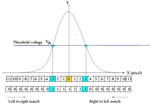
3.3.1 Light spot distribution
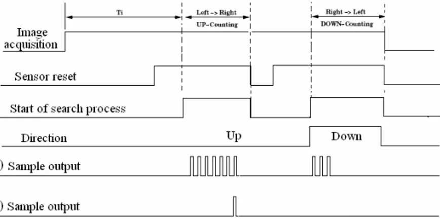
3.3.2 The position detection algorithm 3.3.3 Algorithm implementation 3.3.4 Position to pulse conversion
3.3.4.1 Asynchronous operation 3.4 SUB-PIXEL RESOLUTION
3.5 MULTIPLE IMAGES BINARIZATION
3.6 SEQUENTIAL ARRAY AND PARALLEL SENSOR
3.7 MULTIPLE THRESHOLDING VS. MULTIPLE IMAGES BINARIZATION 3.8 UP/DOWN COUNTING
3.9 PARALLEL TO SERIAL DATA CONVERSION 3.10 TESTING AND TESTABILITY
4 SENSOR DESIGN
4.1 INTRODUCTION
4.1.1 THE 2D VISION SENSOR 4.2 THE LINEAR SENSOR ARRAY
4.2.1 Carryout signal propagation time 4.3 PIXEL ARCHITECTURE
4.3.1 The sensing node capacitance 4.3.2 Comparator block
4.3.3 carryout generation block 4.3.4 Pulse generation block 4.3.5 Functionality of the pixel 4.3.6 Initialization procedure 4.3.7 Search process
4.3.7.1 Forward direction 4.3.7.2 Reverse direction 4.3.8 Layout of the pixel 4.4 PIXEL ARRAY 4.4.1 BIT-LINES 4.5 DIGITAL PROCESSOR 4.5.1 Up/down counter 4.5.2 Shift register 4.6 2D ARCHITECTURE 5 DEVICE TESTING 5.1 INTRODUCTION
5.2 IMAGER BOARD BLOCK DIAGRAM 5.3 SENSOR FUNCTIONAL DIAGRAM
5.4 ELECTRICAL TESTING OF THE LINEAR SENSOR 5.4.1 Testing of functional blocks
5.4.2 Testing of the linear array
5.4.3 Testing of counter and shift register 5.4.4 Testing of linear sensor
5.5 OPTICAL BENCH AND PATTERN GENERATION TEST SETUP 5.5.1 Measurements for multiple images binarization 5.5.2 Image binarization after image integration 5.5.3 Image binarization during image integration 5.5.4 Overlapping image acquisition and processing 5.5.5 Integration time vs. process cycle time
6 MEASUREMENTS AND EXPERIMENTAL RESULTS
6.1 INTRODUCTION 6.2 MEASUREMENT SETUP 6.3 MEASUREMENTS 6.4 ANALYSIS 6.4.1 Standard deviation 6.4.2 Accuracy
6.4.3 Integral non-linearity (INL) 6.4.4 Differential non-linearity (DNL) 6.5 SPOT SHAPE
6.6 THEORETICAL VS. MEASURED POSITION SENSITIVITY 6.7 POST-TESTING SIMULATIONS
6.9 RELATED WORK
6.9.1 Comparative study of state of the art imagers
7 CONCLUSIONS
7.1 OVERVIEW
7.2 CMOS IMAGER WITH A NEW 2D ARCHITECTURE 7.3 REDUCTION IN IMAGE PROCESSING COMPLEXITY 7.4 MULTIPLE IMAGES BINARIZATION- TIME VS. VOLTAGE 7.5 ADVANTAGES OF THE APPROACH
7.6 FUTURE WORK 7.7 APPLICATIONS 8 BIBLIOGRAPHY 9 APPENDIX 10 APPENDIX A 11 APPENDIX B 12 APPENDIX C
Acknowledgements
“Endaro mahaanu bhaavulu, andariki vandanamulu”, in my mother tongue, Telugu, says there are ‘so many great people, I salute them all’.
First of all, I am deeply indebted to Prof. Zorat, my advisor, for his kind guidance, constant encourage-ment and unwavering support during my entire Ph. D program. He has given me several opportunities for professional growth and has always come to my rescue during crisis periods.
I am running short of words to express deep appreciation to my co-advisor, Ing. Massimo Gottardi, for sparing me countless hours of his precious time during all the stages of my research. But for his guidance and untiring efforts, I would not have completed my work. I will always be grateful to him.
I thank the Dean ICT and the Head, DIT for providing me an opportunity to be on the rolls of ICT. I thank Prof. Giancarlo Parodi, University of Genova and Prof. Alessandro Paccagnelia to be on my committee and accepting to review my thesis.
I thank Dr. Mario Zen, Director, ITC-irst for permitting me to work with the disciplined and professional environment of the Microsystems group. I thank Dr. Simoni, group leader, SOI, for providing me the Ca-dence facilities and sponsoring the fabrication of the prototype of my chip. I thank Drs. Lorenzo and David, Nicola, the Viarani brothers, Fabrizio, Stefano, Malfatti and all the members of Microsystems group for helping me whenever I have approached them. This is the friendliest environment I have ever seen. I thank Dr. Dalla Betta and Professor Soncini for introducing me to the group.
I thank Prof. Andreas Andreou and his illustrious group at Johns Hopkins University, Baltimore, USA, for providing me a wonderful opportunity to work with them in the eminent “Andreou lab”. I am always grateful to Prof. Andreas for his kind and exceptional support. My special thanks are due to Philips, Eugenio, Frank and Professors: Ralph-Etienne-Cummings, Paul Sotiriadis and their teams for their sup-port while in JHU.
I also had to face the saddest moment in my life during this program- the sudden demise of my father. The stay in JHU has helped me overcome great part of the grief. The Badminton team at JHU has helped me come out of the solitude.
I thank Mr. Oleg for his timely help in FPGA and VHDL design part of my thesis. I thank all the faculty members, supporting staff and friends in DIT, CISCA, Secretariat, Ph. D office and Welcome office for their prompt support. Thanks are also due to all the colleagues at ICT, University of Trento, ITC-irst and CEERI Pilani for their support.
I would like to thank the peers in the field, through this medium, who have been magnanimous to respond to my queries: Prof. Varanasi and Dr. Harvey Glass, USF; Prof. Sangiovanne Vincentelli, UCB; Prof. Ran Ginosar, Technion; Prof. Paul Allen, GIT; Prof. A.J.P. Theuwissen, Prof. Harry Veendrick and Dr. Ad Peeters, Philips Research; Dr. Alireza Moini, Univ. of Adelaide; Prof. Brian Curless, UW ; Dr. B. Pain, JPL; Ken Chapman & Peter Alfke, Xilinx, Dr. Angelo Beraldin, NRC, IIT, Canada, Y.Oike, Tokyo Univ… and the list is endless. I seek forgiveness from those who spared their professional time to answer me patiently, but whose names I could not mention here.
I thank Director, CEERI, Pilani, and DG-CSIR, India, for their extraordinary gesture in granting me study leave to pursue my Ph. D program in Italy.
I finally thank all my family members in India and USA for their moral support. Special words of appreciation to my wife Padma, and sons Vijayendra and Sai Srinath for allowing me to pursue this venture at a rather late(r) part of life, in a far off land and sustaining on their own during such a long separation. I always remember Italy as the most beautiful country with friendliest people. Trento has been my dream city and truly a home away from home.
Chapter 1
Introduction
Vision is our most powerful sense, which provides us with a remarkable amount of information about our world in three dimensions. It facilitates us to interact with our surroundings intelligently, learn the posi-tion and identities of objects and the relaposi-tionship between them, without requiring any physical contact. Hence, efforts to provide machines a sense of vision to see and react to the situation has always been the thrust in the vision research [BER1].
3D measurements form a major part of vision research. They enable extraction of the 3D coordinate data by means of an image-sensing medium, from the geometry of visible surfaces of the target, and recon-struct its profile information. Examples of 3D measurement applications abound- a robot picking an ob-ject, a space probe collecting samples, an inspection system detecting the solder paste deposits in an elec-tronic assembly, or a shape reconstruction task of a museum object, all require accurate object position or range estimation, often in real time. To capture the complete shape of an object, thousands of samples must be acquired, for which a suitable method of measurement and a high speed and accurate image sen-sor are necessary for reliable image acquisition and processing. While the image from a camera shows the intensity distribution of the viewed scene, a range camera, in contrast, gives the distance from the camera to the objects of the scene.
The range-imaging sensors in such systems are unique imaging devices in that the image data points explicitly represent scene surface geometry as sampled surface points. The inherent prob-lems of automatically interpreting 3-D structure from the output of other types of imaging devices, such as video cameras, are not encountered with range-imaging sensors. Range images are also known as range map, depth map, depth image, range picture, 3-D image etc., depending on the context [BES].
1.1 Optoelectronic methods of 3D imaging
Several optoelectronic techniques for 3D imaging have been proposed in the literature for range imaging: the surveys of [BES, JAR] for range detection are the classic references for 3D imaging researchers. [STR] covered range-imaging techniques from an optical engineering viewpoint. More recently dif-ferent other taxonomies are proposed: while [CUR] suggests difdif-ferent active methods, [DAV] pro-poses a new classification to unify a class of methods in terms of spatial vs. temporal methods.
Range images are obtained in many different ways. Traditionally these are classified into two categories, active and passive range imaging. Figure 1.1 shows one such classification. While the passive rely on ambient environment conditions, the active method uses a coherent light source to project onto the object
in a structured manner and determines the shape of the object by its reflections.
Passive systems require
well-defined features such as targets and edges and have difficulty with sculptured surfaces and
unstructured environments. The computer vision research community is largely focused on
pas-sive methods, which extract shape from digitized images, including shape-from-shading for
sin-gle images, stereo methods for pairs of images, and optical flow methods for video streams
[CUR]. Whereas these methods require very little special purpose hardware, they typically do
not yield dense and highly accurate digitizations required by a number of applications.
1.1.1 Active optical methods
Since the active optical systems provide their own illumination, they can easily measure
sur-faces in most environments.
In contrast to passive methods, many active optical rangefinders canrap-idly acquire dense, highly accurate range samplings.
The active optical systems sample the shape of
image.
These active optical methods include time of flight (ToF), interferometry and triangulation. The following discussion brings out salient features of each method.1.1.1 .1 Time of flight method
In ToF [LAN, ULL, VIA] systems, a projected light is reflected from a target object with some delay proportional to the distance. A camera detects the arrival time of the reflected light to measure the dis-tance. However, despite its apparent simplicity, a laser ToF system is not easy to design in practice. Primarily, the coincidence electronics must accurately measure very short time intervals. Sec-ondly, the power received from the target surface may be very low, which means that the elec-tronic signal generated by the photodetector may be affected by noise [POU]. Thus, the surface property and orientation along with range affect the energy collected by the photodetector. This limits the range accuracy typically to a few centimetres. For smaller objects of <1m in size, attaining 1 part per 1000 accuracy with time-of-flight methods require very high speed timing circuitry, because the time
differ-ences to be detected are in the femto second (10-15 s) range. Hence, this method is generally applied in
long-range 3-D measurement of large objects, such as monuments and buildings.
Figure 1.1: Optoelectronic techniques for 3D imaging
1.1.1.2 Interferometric method
In the interferometric method [BES], a spatially or temporally varying periodic pattern is projected on to the surface of the object. The reflected light is mixed with a reference pattern, which demodulates the sig-nal to reveal the variations in surface geometry. While, moire interferometry involves the projection of coarse, spatially varying light patterns onto the object, the holographic interferometry relies on mixing coherent illumination with different wave vectors to achieve the objective. The angular separation of source and detector is critical to range measurements and therefore, moire can be considered an-other type of triangulation method though it exhibits many similarities to holographic interferometry. Moire methods can have phase discrimination problems when the surface does not exhibit smooth shape variations, which limits the maximum slope the surface can have to avoid ranging errors.
Light Waves 100 THz To 1000 THz Active Passive Triangulation Time delay (Speed of light & Laser co-herence) Silhouettes: photo sculpture Projection: Single spot Moiré
Time of Flight (ToF) Pulsed LIDAR
Interferometry (Optically coherent detection) Multi wave-length Sequential and single fringe pro-jection Colour coded projection Projection: Bundle of rays Continuous modulation (AM, FM,..) Holographic Projection: Sheet beam Speckle or White light based Shape from shading
Steriopsis: Binocular vision
Photogrammetry
Focus/de-focus: Confocal microscopy
1.1.1.3 Optical triangulation method
Optical triangulation is one of the most well known optical rangefinding approaches. In this
method, the location of the centre of the reflected light pulse imaged on the sensor corresponds
to a line of sight that intersects the illuminant in exactly one point, yielding a depth value. By
translating or rotating the object through the beam or by scanning the beam across the object, the
shape of the object can be acquired.
[RIO] presents an innovative approach to triangulation-based range imaging, which shows a synchronized scanning scheme. It allows very large fields of view with small triangulation angles and with high preci-sion. With smaller triangulation angles, a reduction of shadow effects is inherently achieved. The idea is to synchronize the projection of the laser spot with its detection. The instantaneous field of view of the position detector follows the spot as it scans the scene. The focal length of the lens is therefore related only to the desired depth of field or measurement range and not to the field of view. With optical syn-chronization, an improvement in ambient light immunity due to a small instantaneous field of view (long
focal lengths) and a reduction of speckle noise (through spatial filtering) are achieved [BER3].The basic
optical configuration for this large field of view 3D digitizer, is shown in Figure 1.2.
Figure 1.2: Auto-synchronized scanner: dual-scan axis (used equally in triangulation and time
of flight systems) CNR [BER3]
Both mirrors are driven by galvanometers. A raster imaging mode produces a range image of the scene: the x-axis scanner (fast axis) is used for the line scanning while the y-axis (slower speed) deflects verti-cally the scanned beam to produce a raster image. A 3D surface map is obtained by scanning a laser beam onto a scene, collecting the light that is scattered by the scene in synchronism with the projection mirrors,
and finally, focusing this light onto a linear position detector. The image acquisition process yields three quantities per sampling interval: two angular positions of the mirrors and the position of the laser spot on the linear position detector. The equations obtained after the calibration process are used to map the angu-lar position of the mirrors and the laser spot position into (x, y, z) coordinates.
1.2 Comparison of basic active optical measurement methods
The three basic active optical measurement principles: triangulation, interferometry ToF are compared in Figure 1.3, in terms of distance, range and resolution illustrating their suitability for specific applications. The most critical parameters of thes systems are the depth measuring range z and the depth resolutions δz. The figure illustrates the measuring and resolution ranges that are covered by the existing measuring sys-tems. The highest absolute resolutions are achieved by interferometry, which reaches accuracies of λ/100 and can measure ranges up to 10 m using multi-wavelength techniques [CUR]. However, these are very expensive systems. Active triangulation can be used with high resolution from the millimetre range up to several meters where the accuracy depends mainly on depth of field and can be < 10µm for small depths. The ToF techniques allow measurement of depths in the range from tens of cm up to tens of km, but as noted above, the design of these systems could be very challenging [SIM].
All the rangefinding techniques presented here have their specific advantages and drawbacks and none can be considered an overall "optimal" choice [POU]. The 3-D vision system designer must chose the technique best suited for his / her needs. The accuracy and acquisition time are two important issues that a designer has to consider along with the physical dimensions of the rangefinder, which is often of importance, particularly in robotics applications.
Figure 1.3: Performance map showing relative resolution of active 3D optical measurement
methods [SCH]
Though in the past the triangulation systems were considered inaccurate or slow, the state of the systems have become accurate, fast, and compact, mainly owing to the advent of synchronous scan-ning approaches. Triangulation systems go from sequential, as in point scanners, to parallel, as in the
intensity ratio scheme or the color encoded sheet beam scheme. Triangulation systems have been the stronghold of range imaging, and promise to remain so [BES].
Since active triangulation using the sheet beam method is the basis of this thesis, it is discussed in detail in the following sections.
1.3 Active optical triangulation method
In the active triangulation method, the scene is illuminated by a coherent light source from one direction and viewed from another [BES, JAR, MUN, RIO]. Figure 1.4 shows a typical triangulation system and range imaging configuration in 2D. The illumination angle θ, the viewing angle α, and the baseline be-tween the illuminator and the sensor are the triangulation parameters. The variety of the active triangula-tion methods differ primarily in the structure of the illuminant, viz., a single spot or a sheet beam (also known as stripe or sheet of light) or coded light, and the dimensionality of the sensor (linear sensor or 2D structure) and the scanning method, moving the object or moving the scanning mechanism. The shape of the object is acquired by translating or rotating the object through the beam or by scanning the beam across the object.
[DAV] suggests that unifying the various triangulation methods within the space-time [CUR] frame-work allows new hybrid algorithms, ex: temporal stereo, for improved reconstruction of static scenes with unstructured varying (intensity) lighting.
Figure 1.4: Optical triangulation and range imaging showing (i) the triangulation setup in 2D
giving a range value (ii) The 3D setup giving the range image and (iii) the collection of points
showing the range map of the object [CUR]
Figure 1.5 shows the structure of the data, which can be (i) a spot or (ii) a profile of the shape or (iii) a range map of the object. A beam of light forms a spot on the surface and provides a single range value. By passing the beam through a cylindrical lens, a light stripe can be projected onto an object to collect the
Figure 1.5: Structure of data showing point, profile and range imaging concepts [CUR]
range profile and by projecting multiple spots or sheets of light, a range map can be obtained. It may be noted here that frames per sec. (fps) denotes position detection rate on the sensor focal plane. For exam-ple, to achieve 100 x 100 range data for a range map, a range map needs 100 frames for position detection of a scanning sheet beam. 1k fps (frame access rate/position detection rate) corresponds to 10 range maps/s.
1.3 Image sensors in 3D measurement
While the 2D vision is concerned with interpreting a three dimensional environment under a specific il-lumination in other words an intensity profile of light, the 3D vision is concerned with extracting informa-tion from the geometry and the texture of the visible surfaces in a scene. Though the 2D methods are used with reasonable success [SIM] in several industrial applications (ex: whole and partial body scans, reverse engineering of industrial components, reproduction of rare objects, object presence and position-ing etc.,) for acquirposition-ing and interpretposition-ing the 3D data, this mechanism gives only limited information about the detailed shape of an object.
Being the core of a 3D measurement system, an image sensor is required to handle the image acquisition and processing efficiently where speed and accuracy are both critical. A very high frame rate is necessary to reconstruct a range map, which requires thousands of frames per second (fps). For instance, using a spot beam X-Y scanner, a range map with 1M pixels (1024×1024 pixels) requires 1M position detections per range map in a 3D measurement system. Thus, 30M fps position detection is necessary for 30-range maps/s range finding with 1M pixels. A sheet beam scanner can reduce the number of frames for a range map; however, 30k fps position detection are needed to realize a real-time range finding system. Several high-speed CMOS image sensors are reported in the literature, ex: [KLE, KRY], with parallel ADCs re-alizing a maximum of 500- 2000 fps [OIK1].
Since the two important requirements of image acquisition and processing are difficult to meet with stan-dard imagers, it is necessary to develop dedicated vision chips [BRA3, NEZ1, OIK1] with on-chip visual signal processing for achieving the real time functionality in 3D. To achieve this in 3D, generally a 2D imager with specific processing capabilities (known as smart features to address the needs of different applications) performing at very high frame rate is mandatory. CMOS technology enables the develop-ment of these sensors a possibility.
1.3.1 CMOS technology for image sensors
While CMOS is the heart of the electronics industry, the image sensors are the eyes of a whole range of products from toys to complex space stations. With the availability of sub-micron CMOS technologies for
imaging, in terms of the following benefits, a great interest has been focused in recent times on the devel-opment of specialised image sensors [MOI, FOS]:
• Mature technology: CMOS processes have been available for long period and are well developed and well established.
• Design resources: Many design libraries for circuit and logic are supported by various research groups and industries and are readily available for incorporating in the user applications.
• Accessibility: There are many fabs around the world, to fabricate prototype designs at lower prices. • Fabrication cost: Because CMOS process is standardized, the fabrication of CMOS designs is less ex-pensive, compared to other process technologies.
• Power consumption: As CMOS technology scales down, the downscaling of the power supply follows a similar trend, resulting in lower power consumption.
• Compatibility with VLSI circuits: Since CMOS technology is already optimized for logic and mem-ory, it is relatively easy to integrate VLSI circuits with CMOS image sensors.
1.3.2 Smart image sensors or vision sensors
The integration of photosensitive devices with visual information processing elements on the same sub-strate of the device, known as smart image sensors or vision sensors (MOI), represents a select area in machine vision where high performance in terms of frame rates, accuracy and resolution are the most de-manding features. (It may be noted the terminology ‘ smart image sensors’ and ‘vision sensors’ are inter-changeably used in this thesis).
A smart sensor is well defined in “Vision Chips” by [MOI] as following:
“Smart sensors refer to those devices in which the sensors and circuits co-exist, and their relationship with each other and with higher-level processing layers goes beyond the meaning of transduction. Smart sen-sors are information sensen-sors, not transducers and signal processing elements. Everything in a smart sensor is specifically designed for the application targeted for.”
In this thesis, the concept of smart image sensors is further focused on the aspect of the devices in which image sensors and visual processing circuits (beyond signal processing) co-exist, and they interact with each other in order to increase the functionality of the imager chip and the quality of processing.
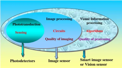
Figure 1.6: Conceptual block diagram of a vision sensor
Image processing Circuits Quality of imaging Visual Information processing Algorithms Quality of processingPhotodetectors Image sensor Smart image sensor or Vision sensor
Phototransduction
Figure 1.6 shows the conceptual block diagram of a vision sensor. While detecting light intensity and transducing it to electrical parameter (phototransduction) is performed by photodetectors (photodiodes, photogates etc.), signal processing circuits such as correlated double sampling (CDS) [WHI], dynamic range enhancement, on-chip clock generation (widely used in camera applications) etc., [DIC1, DIC2,DEC, YAD2] are used to enhance the performance of the CMOS image sensors. However, these do not increase the functionality of the imager chip [MOI].
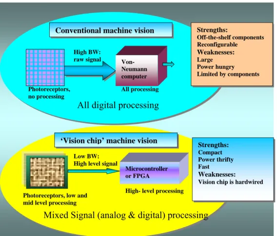
1.3.3 Conventional vs. vision chip machine vision
The smart imagers, on the other hand, address the quality of processing the outputs from the
sig-nal processing stage by integrating algorithms to address specialized applications. They offer
several advantages in terms of speed of processing, cost, size and power dissipation. Figure 1.7
shows the difference between conventional and vision chip approaches of the sensor design
[PAI]. While many conventional image sensors transmit the high throughputs of raw visual data
to a Digital Signal Processor (DSP) for post processing, the vision chip processes the image on
chip and transmits the output (analog or digital) with a low bandwidth, providing a simplified
ex-ternal digital platforms.
Figure 1.7: Conventional vs. vision chip machine vision [PAI]
To sum up the design issues of a vision chip, one should consider several issues including phototransduction to high-level image processing algorithm implementation, from analog to mixed analog / digital to digital design, from analog/digital design to digital noise techniques, from optics to electronics and optoelectronics.
For smart image sensors, CMOS technology is suitable as it enables integration of image sensing and processing logic.
Von-Neumann computer Conventional machine vision
Photoreceptors, no processing High BW: raw signal All processing Strengths: Off-the-shelf components Reconfigurable Weaknesses: Large Power hungry Limited by components
All digital processing
Photoreceptors, low and mid level processing
Low BW: High level signal
Microcontroller or FPGA
High- level processing
Strengths: Compact Power thrifty Fast
Weaknesses:
Vision chip is hardwired
Mixed Signal (analog & digital) processing
‘Vision chip’ machine vision1.3.2.1 Some issues on using CMOS technology for smart image sensors
Since, most of these devices need to be built from scratch due to their specialized nature, this approach is error prone and time consuming. The incorporation of extra features also may result in sacrificing some imaging characteristics, such as resolution, frame rate and power, to enhance the functionality of process-ing [MOI]. Also, because image-sensprocess-ing is relatively a new area for CMOS, the photodetector structures are not well characterized and it is the designers’ responsibility to ensure the photodetector’s functional-ity.
1.4 Smart CMOS image sensor for 3D measurement
The objective of this thesis is to present a smart CMOS image sensor for 3D measurement applications using sheet beam method based on active triangulation. The image sensor is proposed with a 2D architec-ture consisting of N closely packed slices of linear sensors, working independently and in parallel. Each linear sensor, emulating a ‘position sensitive device’ (PSD), estimates the position of the light spot im-pinging on it through centroid estimation. By accumulating the centroids of all the light spots, the 2D sen-sor can reconstruct the profile of the object. As the functionality of linear sensen-sor is replicated in the array in an identical way, the major discussion of the thesis is around a linear image sensor.
1.5 Salient features and scope of the work
The design addresses the 3D imaging problem through N-1D problems thus reducing design complexity. It proposes a novel position to pulse conversion mechanism for image binarization and multiple images binarization to achieve high sub-pixel resolution of position estimation. It also ensures modularity and high level of parallelism in the architecture by implementing the sensor as an array of identical slices. The device presented here is a linear smart sensor as the principle is to be proved in 1D and then extend the same to a 2D architecture.
The following section briefly discusses the organization of the thesis.
1.6 Structure of the thesis
In Chapter 2, a survey of the state of the art in CMOS imaging is presented with an emphasis on imagers used in 3D measurements in general and those using active triangulation techniques in particular.
Chapter 3 consists of the background and the basis for the thesis explaining the concepts used in design-ing the device. These include the stages of signal acquisition and processdesign-ing, centroid algorithm, multiple images binarization, asynchronous mode of operation in position to pulse conversion and concepts of sub pixel resolution.
In Chapter 4, the design of the Smart CMOS imager is presented. Various functional blocks of the device, the implementation of the position estimation algorithm in hardware to calculate centroid of the spot, the array design and the 2D architecture are explained.
In Chapter 5, the testing and testability features of the device are explained. The electrical testing and the test setup with optical bench are discussed. Interfacing with FPGA is presented.
In Chapter 6, the analysis of test results is discussed and a comparison with the related work, mentioned in state of the art, is presented.
Chapter 7 summarizes the work of the research and presents the conclusions derived from this research along with directions for future work.
Chapter 2
State of the art in CMOS image sensors for 3D measurement
2.1 Introduction
This chapter provides a brief background on the range sensors, the triangulation method and of the CMOS based solutions to 3D measurement problems. Though not exhaustive, it covers the historical perspective of devices used in the triangulation-based measurements, viz., PSD (position sensitive device), CCD de-tectors and laser line devices. Subsequently it introduces the developments in CMOS imagers for the spe-cific 3D measurement applications with a review of the state of the art sensors.
2.2 Active range imaging using optical triangulation method
The most common active triangulation methods include illumination with a spot beam and a sheet-beam. After discussing the relative merits of each scheme, this section suggests the method adapted in this the-sis.
2.2.1 Principle of 3D measurement with spot beam projection method
Figure 2.1 shows the spot beam range imaging. A projected spot beam is reflected on a target object and reached on the sensor plane. Therefore, in order to obtain an MxN image MxN measurements have to be made. The range data of a target object are acquired by triangulation with the projected beam direction and the position of incident beam on the sensor plane.
Figure 2.1: Spot beam range imaging [IVP]
The principle of triangulation-based range calculation is shown in Figure 2.2, in which a light source and
a sensor are placed at a distance of d. A scanning mirror provides α1 and θ as a direction of projected
beam. θ can also be provided from the Y position of projected beam on the sensor plane. When a target
object is placed at R(XR, YR, ZR), the position sensor detects the reflected beam at e(xe, ye).
Light source
X-Y axis scanning
1D sensor
Z
X
Y
Figure 2.2: Principle of triangulation based range calculation [OIK1]
α2 and θ are given by
e
x
f
=
2tan
α
(2.1) ey
f
=
θ
tan
(2.2)where f is focal depth of the sensor. α1 and α2 are given by
p
x
d
l
−
=
2
tan
α
1 (2.3) px
d
l
+
=
2
tan
α
2 (2.4)here l is length of a perpendicular line from R to X axis. Hence, XR and l are given by
) tan (tan 2 ) tan (tan 2 1 2 1
α
α
α
α
+ − = d xR (2.5) 2 1 2 1 tan tan tan tanα
α
α
α
+ = d l (2.6)2 1 2 1 tan tan sin tan tan
α
α
θ
α
α
+ = d YR (2.7) 2 1 2 1 tan tan sin tan tanα
α
θ
α
α
+ = d ZR (2.8)The range image of the target scene can be acquired by the range calculation using whole position detec-tion of a scanning beam.
2.2.2 Principle of 3D measurement with sheet beam projection method
In this method, a sheet beam is scanned [IVP] over the scene and one row with N values is acquired at each light position, as shown in Figure 2.3. Using the projected beam direction and the position of incident beam on the sensor plane, the range data of a target object are acquired by triangulation. X-axis being the scan direction, the sensor detects the centre line positions of an incident sheet beam on the sensor plane. Since the 3D measurement system with sheet beam needs just N frames, it reduces the num-ber of required frames for a range map of position detection with N×N pixel resolution. Though it enables to realize a high-speed range finding system, more pixels are activated on the sensor plane than that of a spot-beam-projection system.
Figure 2.3: Sheet of light range imaging [IVP]
Ranger
For each position of the sheet beam, the depth variation of the scene creates a contour, which is projected onto the sensor plane. If we extract the position of the incoming light for each sensor row, we obtain an offset data vector, or profile, that serves as input for the 3D computations.
To make a sheet beam sharp, the laser spot-light passes through a lens. The lens spreads the light into a sheet in one dimension while it is unaffected in the other. The two-dimensional range images can be ob-tained in three ways: by moving the apparatus over a static scene, or by moving the scene, or by sweeping the sheet beam over a static 3D-scene using a mirror arrangement. In the first two cases, the distance can be computed from the offset position in each row using a simple range equation. However, in the third
Light source X axis scanning 2D sensor Z X Y
case, since the direction of the emitted sheet beam changes, a second triangulation parameter becomes in-volved for each light sheet position, which is not desirable.
Ranger
For each illumination position and sensor integration, the output from the 2D image sensor should be re-duced to a 1D array of offset values. Many commercial sheet beam range imaging systems [BLA, MAL] are based on video-standard sensors, with a preset frame-rate (50 Hz in PAL standard) limiting the range profile frequency to 50 Hz. A 512x512 range image is then obtained in 10 seconds, and the range pixel frequency is 25 kHz. Even if the frame rate could be increased, the sensor output is still serial, which would require very high output and processing clock frequencies and possibly increase the noise level [IVP].
The spot beam technique requires advanced mechanics to allow the spot to reach the whole scene. At least two synchronous scanning devices are required. The advantage is that a relatively simple linear sen-sor, e.g. of the position sensitive device type, can be used. However, the use of only one single sensing element often reduces the acquisition speed. In the case of sheet beam systems, the projection of the light can be done with one single scanning mirror.
D
The optical triangulation based on the sheet beam method is the most suitable in terms of cost, complexity and resolution for mid-range 3D measurement systems, as it offers < 1 mm range finding at a distance of several meters, and high robustness of measurement environment due to active range finding. Future 3D applications like advanced gesture recognition systems, accurate shape measurements, 3D pictures and scientific observations require the high speed and high resolution imagers [OIK1].
2.3 Range sensors
A range sensor measures the distance between a reference point and a specified target. Therefore, a range image is a large collection of distance measurements from a known reference coordinate system to surface points on object(s) in a scene. If scenes are defined as collections of physical objects then surface points are defined as the 3-D points [BES].
The applications of range sensors can be divided into two categories: (i) finding the distance to the closest object and (ii) determining the general shape characteristics. Whereas robot navigation and obstacle avoidance are examples of the first category, depth map applications belong to the second. Algorithms with low computational complexity can realize the distance measurements, while depth map requires that every point on the object be identified precisely to obtain the shape. Hence, most of the time, complex mathematical methods are used to realize such systems.
Sensor viewing constraints are the primary issues to be addressed in range imaging sensor requirements. In [BES], four basic types of range sensors are distinguished, based on the viewing constraints, object movement possibilities and scanning mechanisms: “
• A point sensor measures the distance to a single visible surface point from a single viewpoint along a single ray. A point sensor can create a range image if (i) the scene object(s) can be satis-factorily "scanned" in two orthogonal directions in front of the point-ranging sensor, or (ii) the point-ranging sensor can be scanned in two directions over the scene, or (iii) the scene object(s) are stepped in one direction and the point sensor is scanned in the other direction.
• A line sensor measures the distance to visible surface points that lie in a single 3-D plane that contains the single viewpoint or viewing direction (method also known as light sectioning). A line sensor can create a range image if (I) the scene object(s) can be satisfactorily "scanned" in the direction orthogonal to the sensing plane, or (2) the line ranging sensor can be scanned over the scene in the orthogonal direction.
• A field-of-view sensor measures the distance to many visible surface points that lie within a given field of view relative to a single viewpoint or viewing direction. This type of sensor creates a range image directly. No scene motion is required.
• A multiple-view sensor locates surface points relative to more than one viewpoint or viewing di-rection because all surface points of interest are not visible or cannot be adequately measured from a single viewpoint or viewing direction. Scene motion is not required.
These sensor types form a natural hierarchy: a point sensor may be scanned (with respect to a sensor axis) to create a line sensor, and a line sensor may be scanned (with respect to the orthogonal sensor axis) to create a field-of-view sensor. Any combination of point, line, and field-of-view sensors can be used to create a multiple-view sensor by rotating and translating the scene in front of the sensor(s).” [BES]
Range-imaging sensors are the data-gathering components of range-imaging systems, which themselves are the machine-perception components of application systems. Algorithms, software, and hardware are typically developed in isolation and brought together later, but by incorporating programmability features in hardware, (ex: vision chips) the operation of the application systems can be expedited.
2.4 Triangulation sensors: An overview
Triangles are the basis of many measurement techniques, from basic geodesic measurements performed in ancient Greece to more modern laser-based 3D cameras [BER3]. The Greek philosopher Thales (6th
century BC) has been credited with the discovery of five theorems in geometry (www.britannica.com),
two of which are used to solve the triangulation equations in a range camera. They state that opposite an-gles of intersecting straight lines are equal and a triangle is determined if its base and the anan-gles relative to the base are given ( Figure 2.4). Choosing one of the three laws, i.e. sines, cosines and tangents, solves the last theorem.
Figure 2.4: Similar triangles and cosine law [BER3]
While the principle of optical triangulation has been known for centuries (invented by Gemma Frisius in 1533), the use of triangulation for automated measurement is a relatively new technology. This is not be-cause of knowledge of how to make a sensor but rather bebe-cause of availability of suitable components. During the 70’s the practical triangulation sensors for industrial applications have started becoming avail-able, enabled by the commercialization of solid-state detectors and early microcomputers.
Triangulation sensors are widely used for inspection of dynamic materials [PAS], such as monitoring tyre dimensions while rotating at high-speed, closed loop control of pouring of molten metal and 3D contour-ing profiles of logs and boards. Laser triangulation sensors are also ideal for monitorcontour-ing vibrations, with-out adding the mass of a sensor to a component, which would alter the vibration characteristics of the ob-ject.
The triangulation sensors generally use light source of relatively high intensity, such as laser. Since trian-gulation requires finding the location of the centre of the imaged spot, the imaging detector must be capa-ble of detecting the spot location. Traditionally, there are two types of solid-state detectors: position sensi-tive device (PSD) detector and the charge coupled device (CCD) detector.
2.4.1 PSD Detectors
The PSD is an analog detector [PAS], which relies on the current generated in a photodiode and converts incident light into continuous position data, with outputs at both ends, A1 and A2. The output current is proportional to the reflected light spot’s position on the detector. If the reflected light is in the middle of the detector, the analog outputs at each end are equal, but as the light moves from the centre of the detec-tor, the outputs change proportionally. The receiving element finds the position of the centre of the aver-age light quantity distribution. There is no other information that the PSD element can provide.
Figure 2.4: Position sensitive detector
Disadvantages of the PSD include lack of ability to display an image or profile of the detector pattern. Also, the PSD determines the centre of all light that falls on the detector area. If more than one spot or other light falls on the detector, it will report the position of the centre of all light, as if the center of grav-ity of the light spot is shifted, possibly giving an erroneous signal. Another consideration is that PSD sys-tems are sensitive to light intensity. This is inherent in the detector. If the light intensity changes and the spot position remains the same, the output changes. This is the net effect when the target’s colour changes.
2.4.2 CCD Detectors
A CCD is basically an array of closely spaced MOS diodes, in which the light is recorded as an electric charge in each diode. Under the application of a proper sequence of clock voltage pulses, the accumulated charges can be transferred in a controlled manner across the semiconductor surface to the output of the device. The output contains information on the light quantity distribution all over the active area. In the point triangulation sensors [PAS], a single dimension CCD is used, as shown in Figure 2.5.
Laser spot
A1 A1
Figure 2.5: CCD detector
Figure 2.6 illustrates the light intensity distribution and position detection with a CCD element and an analog PSD element. Colour changes and stray reflections result in position-detection errors when a PSD element is used. On the other hand, the CCD element gives the exact position regardless of target colour, tilt, or stray reflections. Disadvantages of the CCD detector are related to speed of operation, which typi-cally is less than that can be achieved with a PSD. Gain control in CCD based sensors is not as fast as in PSD based sensors, a drawback in applications where surface reflectivity changes rapidly.
Figure 2.6: PSD vs. CCD [DUM]
2.4.3 Laser line sensors
A better version of the CCD based detector is commercially available (ex: L1 sensor family- LMI Inc.)
Using a 2D CCD as the detector, this sensor collects multiple points in a frame generating the contour of the surface, as shown in the Figure 2.6. If the part is moving under the sensor, a 3D map of the surface can be generated.
However, this approach is slower in data acquisition rate than a single point triangulation sensor, and typically provides medium accuracy specifications. It also requires that part surfaces be reasonably uni-form in reflectivity, since gain control can only be provided over the full field of view.
This discussion points out that these sensors are not suitable for real time 3D measurement applications, where speed and high accuracy of position estimation are both important. The following discussion briefly gives the state of the art in CMOS imagers for 3D applications with active triangulation as the method of measurement.
2.5 Image sensors for 3D measurement
3D measurements are concerned with acquiring geometrical shape of the object in contrast with the 2D imaging, where only local reflectivity is the matter of concern. The vision sensors used for the 3D imag-ing applications may consist of CCD or CMOS image sensors / processors, which in turn may be made of arrays of pixels, or columns or processor cores with processing elements (also known as vision system on chip VSOC). The output often is not images but information for decision-making. Several factors are to be considered for the design of a 3D imager to work in real time. The design of the chip can take any of the following forms:
(i) Chip level processing: where a processor core (mostly off-the-shelf) and sensing elements are
interfaced in a single casing for performing vision tasks
(ii) Column level processing: where one processing element for each column of the array is used
for undertaking local processing, and
(iii) Pixel level processing: where each pixel in the array contains its own processing element.
[PAI] illustrates the approaches of VSOC and the related advantages and disadvantages.
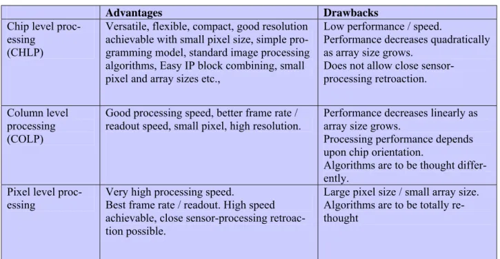
Table 2.1: Vision system on chip: comparison of processing
Advantages Drawbacks
Chip level proc-essing
(CHLP)
Versatile, flexible, compact, good resolution achievable with small pixel size, simple pro-gramming model, standard image processing algorithms, Easy IP block combining, small pixel and array sizes etc.,
Low performance / speed.
Performance decreases quadratically as array size grows.
Does not allow close sensor-processing retroaction. Column level
processing (COLP)
Good processing speed, better frame rate / readout speed, small pixel, high resolution.
Performance decreases linearly as array size grows.
Processing performance depends upon chip orientation.
Algorithms are to be thought differ-ently.
Pixel level
proc-essing Very high processing speed. Best frame rate / readout. High speed
achievable, close sensor-processing retroac-tion possible.
Large pixel size / small array size. Algorithms are to be totally re-thought
Table 2.2 shows the merits of single chip integration single chip vs. separate chips for sensor and process-ing. Though the comparisons in the reference are mainly with reference to VSOCs, they also are applica-ble to the vision chips used in 3D measurements.
Table 2.2: Single chip integration vs. separate sensor / processing
Criteria Single chip integration Separate chips for sensor and process-ing
Power (+) Only minimum hardware
integrated. No inter-chip communication which wastes power, optimal use of parallel-ism / low frequency require-ment, low voltage
(-) General purpose chips, involving un-necessary functionalities, energy wast-age, high frequency needed, high power chip-to-chip communication: wastes en-ergy
performance (+) Parallelism integrated at
pixel level, high speed, high frame rate
(-) High latency data access, sensor to processing chip bottleneck
Accuracy (-) Sensing / processing quality
trade-off
(+) Sensor chip only, so no processing noise, optimised for best sensitivity / ac-curacy
Volume / size (+) Single chip : most compact (-) Few chips
cost (+) Single chip, standard
CMOS process
(-) Costly CCD process, multiple chips, casing and board integration
(+) advantage and (-) drawback
Most smart sensors cited in the literature, follow the pixel level processing and are implemented as single chip solutions. The following discussion presents analysis of the state of the art smart imagers for 3D measurement using triangulation methods.
2.6 State of the art smart sensors for 3D measurement using active triangulation
Almost all the 3D measurement applications, in the present context, rely on the accurate computation of the centroid. Low power, high-speed, accurate computation of centroid in the image plane is also impor-tant for many applications including: object tracking in robotic systems [BER2], autonomous navigation [ZUF], space guidance and navigation systems [SCH2], and deep-space optical communication systems [ALE] that require accurate and stable beam pointing for high speed data transfer. Off-focal-plane digital processors yield accurate centroid values, but only at the cost of increased latency, power and size [PIE]. On or near focal plane centroid computation using current mode circuits and neuro-MOS circuits have been implemented [DEW]. However, neither approaches are integrated with high performance image sen-sors, nor are they entirely compatible with one [SUN].
A range finding chip [GRU] with cell parallel architecture is proposed for parallel sheet beam range detection. When the beam passes over a photodetector, a current pulse is generated. The position of the pulse, in time, gives a measure of the range. It is reported that 1000 frames per second is achieved with 0.5 mm accuracy. However, this falls short of the real time 3D requirement in terms of frame rate and accuracy.
The commercial photodiode arrays, often used in 3D vision sensors, are intended for 2D imaging applica-tions, where the specifications change according to the evolution of their respective fields and not related to digital 3D imaging. For example, speckle noise dictates a large pixel size [BAR] that is not compatible with current 2D imaging developments (where pixels are getting smaller). Many devices have been built or considered in the past for measuring the position of a laser spot, viz., continuous response position sen-sitive detector (CRPSD) and discrete response position sensen-sitive detector (DRPSD) [MAY]. While a CRPSD provides the centroid information in continuous mode, very precisely, a DRPSD (detectors im-plemented in CCD or CMOS), on the other hand, provides information relative to the spot position with a higher accuracy, but is slower [BER4]. Since accuracy is more important than precision, a DRPSD is generally preferred. An integrated approach combining CRPSD and DRPSD [SIM] is proposed for achieving good precision with high accuracy. However, these cannot integrate smart features and hence not efficient in terms of quality of image processing nor can achieve the speeds anticipated for real time needs.
A high speed position sensitive detector is reported in [MAS], employing analog intensive parallel com-putation for the estimation of the position of the centroid of the light spot. The centroid detection algo-rithm is based on binarization. Though this device cannot be compared with a 3D measurement applica-tion, the algorithm implemented in this thesis has roots in this design. However, the similarity ends there. The central nervous system uses asynchronous pulse coding to share the results among neurons in the brain [KOC]. It will be interesting to investigate if this strategy can be used in the vision chips. The out-put of any photoreceptor array is usually scanned serially and the entire image is read out for processing, no matter whether anything of interest happened in the interval. Thus, each pixel in the image gets a fixed fraction of the total communication and processing bandwidth. However, this will be a waste of bandwidth. A more intelligent strategy would be to send out a signal only when an event has occurred, as that happens in most parts of the brain. Multi-chip systems based on such asynchronous communication protocols have been designed by a number of researchers [AND, BOH, CUL, LAZ, SHI, VIT], to name a few. Individual pixels generate a pulse (or spike, in the language of neurobiology) that is assigned a unique address and placed on a bus. The chip that receives the retina output then knows that something of interest has happened at that address.
There is a similarity between this thesis and the references cited here as far as the concept of asynchronic-ity and pulse based approach is concerned. However, this thesis does not have any leaning towards bio-logical inspiration, nor contains concepts of analog neural processors. Nevertheless, the advantage of us-ing spikes or pulses is explored in the device design.
Some conventional high-speed position sensors have been reported in [BRA1, BRA2, BAK, YOS, SUG] which are developed for range finding, based on the sheet beam method. A computational sensor is pro-posed in [BRA1] to increase the process speed by selecting the sub-regions of the image that require processing, pre-process them and transmit the data only from the sub-regions. The sensor uses a row-parallel winner-take-all (WTA) circuit and can acquire a 64×64 range map in 100 range maps/s. However, the pixel resolution is limited by the precision of the current mode WTA circuit. Thus, it is difficult to re-alize this sensor for real time range finding with high pixel resolution.
The sensor using pixel-parallel architecture [YOS] achieves 192×124 range finding in video rate. It has a large pixel circuit for frame memories and an ADC. To reduce the pixel size, a 320×240 (QVGA) colour imager is developed with analog frame memories [SUG]. Though it makes a pixel circuit smaller and re-alizes 160×120 3D imaging in 15 range maps/s, the range finding rate is inferior to [YOS]. Hence, it is also difficult to get a 3D image in real time with higher pixel resolution.
A position detection sensor for 3D measurement, reducing the number of cycles for position detection is reported in [NEZ1], when activated pixels exist locally on the sensor plane. The operation cycles are
given as O(log2N) theoretically. In [NEZ2], which has a row parallel sensor architecture, it is reported
operation with 75 range maps/s at 0.5 sub-pixel resolution. The device proposed in this thesis projects the order of range maps suitable for 3D measurement along with high sub- pixel resolution.
In [OIK1], a high-speed position sensor using quad-tree scan is introduced, which has the capability of 10k points/s position detection of a projected spot beam. Three other position sensors for a high speed range finding system with sheet beam projection are reported, which include two row-parallel architec-tures for quick position detection on the sensor plane and a real-time 3-D image sensor with high pixel resolution is presented. It employs a high-speed readout scheme with adaptive threshold circuits, which allows a compact pixel circuit implementation for over-VGA pixel resolution. [OIK2] presents an im-proved version of the chip mentioned in [OIK1]. Though no claim is made in this thesis on surpassing these chips, by careful observation it will be apparent that the design used in this thesis is much simpler and has some unique approaches in the architecture implementation.
2.7 Conclusions
In this chapter, spot beam and sheet beam based triangulation methods are described. The characteristics of range sensors are discussed. For historical perspective, triangulation sensors comprising PSD, and CCD detectors and commercial laser line sensors are introduced to underline the evolution of the position detection sensors. For 3D measurements in real time, these devices are not used as they do not match the speed and resolution criteria. The vision processing methods are compared and the advantages of single chip vs. multi chip approach are briefly discussed. The need for dedicated vision chip for performing spe-cific task is highlighted, paving way for the smart sensor design. State of the art smart imagers are re-viewed in order to compare the design presented in this thesis. A comparative chart will be presented in the results and analysis chapter to compare the salient features of various designs.
Chapter 3
The Background
3.1 Introduction
This chapter introduces the concepts behind the design of the vision sensor in the context of sheet beam based 3D measurement using active triangulation methods. The design involves addressing wide ranging issues from implementing a suitable visual processing algorithm in CMOS VLSI for the 3D measure-ments on one end (at the highest level) to acquiring the image information by a photoreceptor on the other end (at the lowest level).
In the following sections, the design criteria are discussed. The chapter on Sensor design is based on these foundations. Subsequently, pixel level processing and image binarization with non-conventional A/D conversion are discussed. The advantages of this early digital approach are highlighted.
3.2 Design criteria and guidelines
Pixel is the basic building block of a vision sensor, which carries out the phototransduction to process the incident light from the scene into a measurable electrical signal. The output of the pixel is then processed in order to interpret the scene characteristics. In addition to the photodetecting and image acquisition circuits, a vision chip requires analog conditioning and processing circuits, digital processing and interfacing, and image readout circuitry all on the same chip. The vision chip may contain several (order of hundreds) arrays of the photodetectors along with the processing circuits. In most cases of the imager implementations, these components should interact with at least their nearest neighbours. This involves a close interaction of the optoelectronics, and electronics parts of the device, which contains photodetectors, analog, digital and mixed mode elements. Additionally, a vision chip for 3D measurement has to implement the visual processing algorithm of the imaging task.
To design a vision sensor for 3D measurement, in this context, one has to consider several
is-sues: how soon the incident light, converted in to analog voltage by the photodetector, can be
transformed into digital domain for efficient data processing; what should be the form of the
out-put data; how efficiently the data can be handled; how to implement the search algorithm on the
focal plane of the device to detect the centroid of the light spot precisely; how to process the
data and output the same to further stages of the image processing chain; and finally how to
in-terpret the output data.
The use of pulses for computation has good potential [WAT] in the circuit design. Circuit
im-plementations using continuous analog signals are subject to noise and will be especially
prob-lematic when the signals must be communicated across the chip boundaries. A pulse-coded
process can use a single wire for communication like analog voltages and currents, but retains
noise immunity of digital signals. Using simple digital techniques, binary pulses can be buffered
and transmitted without loss of performance. Pulse based approach can effectively exploit the
best features of both analog and digital circuits.
Secondly aiming at high modularity and parallelism in the design by means of pixel and column level processing, the architecture becomes reusable, replicable and trouble shooting can be easier. These are discussed in the chapters on design and testing.
Keeping the above mentioned issues in view in the design of the vision sensor, the following parameters have been considered:
• Transform the analog photo signal into digital at the earliest in the image processing cycle • Interpret the position of the pixel in pulses and binarize the information
• Implement the centroiding algorithm for identifying the position of the light spot • Achieve high modularity and parallelism in the architecture,
• Combining the processing of pixel level and column level architectures to take advantage of both the domains in terms of speed and resolution and
• Process the sensory information serially in the array and in parallel at the sensor level The following sections discuss on the issues presented here.
3.2.1 Photodiodes in standard CMOS process
A p-n junction diode is a CMOS compatible device, which can be used as photodetector in image sensors. In a standard CMOS process, several structures can be formed to convert light into an electrical signal. These structures, which are mainly junction devices, are shown in Figure 3.1 for an n-well process (the complementary structures are obtained in a p-well process).
![Figure 1.3: Performance map showing relative resolution of active 3D optical measurement methods [SCH]](https://thumb-eu.123doks.com/thumbv2/123dokorg/2949111.23384/11.892.166.651.576.1040/figure-performance-showing-relative-resolution-optical-measurement-methods.webp)
![Figure 1.5: Structure of data showing point, profile and range imaging concepts [CUR]](https://thumb-eu.123doks.com/thumbv2/123dokorg/2949111.23384/13.892.267.661.102.351/figure-structure-showing-point-profile-range-imaging-concepts.webp)
![Figure 3.3: Simulated quantum efficiency versus wavelength for three different junction diodes in a 2 µm process [MOI]](https://thumb-eu.123doks.com/thumbv2/123dokorg/2949111.23384/31.892.117.479.102.394/figure-simulated-quantum-efficiency-wavelength-different-junction-process.webp)