UNIVERSITY OF ROME
“TOR VERGATA”
Faculty
ELECTRONICS ENGINEERING
Ph.D.
TELECOMMUNICATIONS AND MICROELECTRONICS
ENGINEERING
Ph.D. Cycle
XXII
Organic Photo-Voltaic Cells and
Photo-Detectors based on
Polymer Bulk-Heterojunctions
Ph.D. student
Luigi Salamandra
Tutor
Coordinator
Prof. Aldo Di Carlo
Prof. Andrea Reale
Prof. Francesca Brunetti
Prof. Giuseppe Bianchi
A
BSTRACT
In the last few decades, the use of organic materials for the realization of electronic devices has gained the attention of many research groups. This is mainly due to the possibility to use low-cost techniques for fabrication as solution-processing, suitable also to flexible substrates, and to tailor the material properties for specific applications. In the field of optoelectronics, the use of such materials for the realization of light sources (OLED, Organic Light-Emitting Diode, or OTFL, Organic Thin-Film Lasers), photo-diodes and solar cells has already been demonstrated. In this context, the combination of different organic devices for integrated optical systems, can pave the way to new applications in the field of data communication, sensing application, imaging and solar energy. Conjugated polymer bulk-heterojunction photo-voltaic device made from blend solution could be a good promise for solar energy conversion and data communication purpose, with its solar conversion efficiencies up to ~5% and a time-resolved response of ~200KHz to an optical source.
A
CKNOWLEDGEMENTS
I want to thank Damiano Musella and all the people in ISCOM Laboratories, for training and helping me during my Ph.D. first year; OptoLab and CHOSE colleagues (specially Stefano Penna, Francesca Brunetti, Daniele D‟Ercole, Lucio Cinà, Mauro Mineo and Angelo Lembo) for help and support; Antonio Cardone from PRIN2007 project, for material supplying.
I
NDEX
INTRODUCTION ... 6
CHAPTER 1-POLYMER BULK-HETEROJUNCTION SOLAR CELL ... 8
1.1 - Photo-voltaic effect in organic solar cells ... 9
1.1.1 - General parameter of a solar cell... 9
1.1.2 - Exciton binding energy ... 10
1.1.3 - Single-layer ... 11
1.2 - Heterojunction ... 12
1.2.1 - Double-layer ... 13
1.2.2 - Bulk-Heterojunction ... 14
1.2.3 - Fullerene derivatives as organic acceptor materials ... 15
1.3 - Active layer ... 17
1.3.1 - P3HT:PCBM blend ... 17
1.3.2 - Morphology ... 17
1.3.3 - Weight ratio (X:Y) ... 18
1.3.4 - Solvents ... 18
1.3.5 - Annealing treatments ... 18
1.3.6 - Thermal annealing ... 19
1.3.9 - Layer thickness ... 23
1.3.10 - Influence of molecular weight and regio-regularity ... 24
1.4 - Breaking the η≈5% ... 25
1.4.1 - Ideal donor polymer ... 25
1.4.2 - Ideal acceptor fullerene derivative ... 28
1.4.3 - Additives ... 28
1.4.4 - Tandem solar cells ... 30
1.5 - Stability of BHJ devices ... 33
CHAPTER 2-REALIZATION AND CHARACTERIZATION ... 34
2.1 - Experimental ... 35
2.2 - Patterning of electrodes ... 38
2.2.1 - Wet-etching ... 38
2.2.2 - Laser-scribing ... 40
2.2.3 - Evaporation ... 42
2.3 - Hole transporting layer ... 42
2.4 - Active layer ... 44
2.4.1 - Solid content ... 45
2.4.2 - Weight ratio (X:Y) ... 46
2.4.3 - Thickness ... 47 2.4.4 - Thermal annealing ... 48 2.5 - Encapsulation ... 51 2.6 - Other experiments ... 53 2.6.1 - FTO ... 53 2.6.2 - PET-ITO... 54 2.6.3 - Airbrush ... 55
2.6.4 - Characterization of a new donor polymer ... 57
CHAPTER 3-ORGANIC PHOTO-DETECTOR ... 60
3.1 - All-organic optical data link ... 60
3.2 - Characterization of organic device as photo-diode ... 62
3.2.1 - Plastic optical fiber ... 62
3.2.2 - Green-LED for device characterization ... 63
3.3 - Time-resolved photo-current response ... 64
3.3.1 - Set-up of time-resolved response for OPD ... 64
3.3.2 - Green-LED driver ... 66
3.3.3 - OPD current-voltage converter ... 66
3.3.4 - Max frequency ... 67 3.3.5 - Parasitic capacitance ... 67 CONCLUSION ... 69 APPENDIX ... 70 Evaporator plate ... 70 LIST OF ACTIVITIES ... 73 Articles ... 73
Orals and posters ... 73
Ph.D. schools ... 74
Conferences ... 74
Projects ... 74
I
NTRODUCTION
For most of their history, polymers have been considered as electrical insulators. It was the discovery in 1977 by the groups of Heeger, Shirakawa and MacDiarmid that doped polyacetylene could achieve metallic conductivity which initiated intense research on conjugated polymers[1]. The work of these three pioneers was later honored with the Nobel Prize in Chemistry in 2000[2-4].
While initial research was concentrated mostly on improving the conductivity of conjugated polymers by chemical doping, serious interest also grew in intrinsically semiconducting and highly soluble polymers. From then on, the application of conjugated polymers for a wide range of semiconductor devices such as light emitting diodes (LEDs)[5,6], solar cells (SCs)[7,8] and thin film transistors (TFTs)[9] was systematically investigated.
Nowadays, organic materials in general, and semiconductor polymers in particular, has completely revolutionized the business perspectives of electronics. Thanks to intrinsic low-costs, both of raw materials and manufacturing, possibilities of tailored properties for desired applications, and realization of electronic devices on flexible substrates, first new devices, now commercial products have sprouted.
Sony, Samsung, LG and many other companies are ready to commercialize first
TVs with screen made entirely of organic light emitting diodes (OLEDs). Their features are, first of all, compactness (thickness of few millimeters) and lightness. Plastic Logic have announced the oncoming sale of them electronic papers. Solarmer and Konarka
Power Plastic will soon produce flexible polymer solar cells for many applications
(fig. 1).
Figure 1 – Examples of possible products with flexible organic solar cells.
This work will show the realization and characterization of an organic photo-voltaic device of bulk-heterojunction type, made with solution-processing technique (spin-coating), starting from organic materials dissolved. In the first chapter, the key features of organic photo-voltaic devices will be described, with a notice to the state-of-the-art, while in second and third chapters the use of the photo-voltaic device, both as solar cell and photo-detector, will be showed.
C
HAPTER
1
P
OLYMER
B
ULK
-H
ETEROJUNCTION
S
OLAR
C
ELL
The harvesting of energy directly from the sunlight using photo-voltaic (PV) technology is almost recognized as a key element of future global energy production. PV devices can be made economically competitive with fossil fuels and other emerging renewable energy technologies, and their large-scale manufacturing offers a sustainable energy source that can supply a significant fraction of our daily energy needs.
Photo-voltaic cells have become extensively studied since the 1950s, when the first crystalline silicon solar cell, which had an efficiency of 6%, was developed at Bell Laboratories[10]. Since then, the efficiency has reached 24% for crystalline Si solar cells[11], which is close to the theoretical predicted upper limit of 30%[12,13]. Over the years, solar cells have been made from many other semiconductor materials with various device configuration, such as single-crystal, polycrystalline, and amorphous thin film structures.
Organic materials with semiconductor properties bear the potential to develop a long-term technology that is economically viable for large-scale power generation based on environmentally safe materials with unlimited availability. Organic photo-voltaic devices (OPVDs) have gained a broad interest in the last few years due to their potential for large area low-cost solar cells. From the first reports on molecular thin film devices more than 30 years ago, their power conversion efficiencies have increased considerably from 0.001% in 1975[14] to 1% in 1986[8], and more recently up to ~5% in
2006[15-21]. The progresses in efficiency will possibly make them a competitive
less-expensive alternative to inorganic solar cells in the near future. Organic semiconductors have extremely high optical absorption coefficients compared to inorganic ones, like Si, providing the possibility for the production of thinner solar cells. Additional attractive features of OPVDs are the possibilities for large area, ultra-thin, flexible and low-cost devices, which can be fabricated with organic polymers using high-throughput, low-temperature approaches that employ well established solution-processing techniques, such as spin-coating[22], screen-printing[23], spray-coating[24], ink-jet printing[25], doctor-blading[26], perhaps embedded in a roll-to-roll process[7,27]. This possibility of using flexible plastic substrates in an easily scalable high-speed printing process can reduce the balance of system cost for OPVDs, resulting in a shorter energetic pay-back time.
1.1 - Photo-voltaic effect in organic solar cells
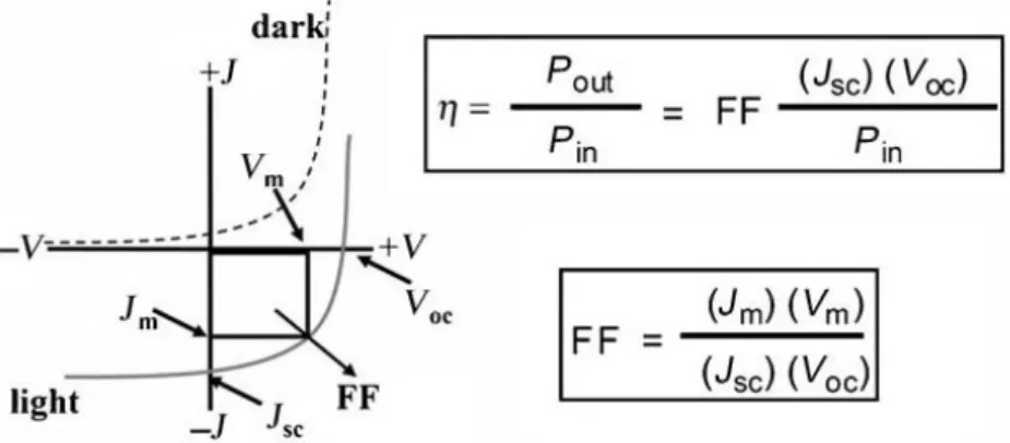
1.1.1 - General parameter of a solar cellThe electrical performance of a photo-voltaic solar cell is characterized by short-circuit density current JSC (often simply noted as ISC), open-circuit voltage VOC and
fill-factor FF. Higher values of these three parameters yield larger light-to-electron power conversion efficiencies η (see fig. 2). Thus, the device efficiency can be enhanced by implementing fabrication procedures that suitably influence JSC and FF (VOC is
Figure 2 - The typical current–voltage (I-V) characteristics for dark and light current in a solar cell illustrate the important parameters for such devices: JSC is the short-circuit current density, VOC is
the open-circuit voltage, Jm and Vm are the current and voltage at the maximum power point, and
FF is the fill-factor. The efficiency (η) is defined, both simplistically as the ratio of power-out (Pout)
to power-in (Pin), as well as in terms of the relevant parameters derived from the current–voltage
relationship.
1.1.2 - Exciton binding energy
Organic solar cells belong to the class of photo-voltaic devices known as “excitonic” solar cells, which are characterized by strongly bound electron–hole pairs (excitons)[28]. Upon absorption of a photon of sufficient energy by the organic semiconductor, an electron is promoted into the lowest unoccupied molecular orbital (LUMO), leaving behind a hole in the highest occupied molecular orbital (HOMO). However, due to weak intermolecular forces that localize the carriers on the molecules, strong electrostatic interactions affect this electron-hole pair, resulting in the production of a mobile excited state (exciton), rather than free electron–hole (e–h) pairs, as in inorganic semiconductors. The exact binding energy of excitons is still under debate, but it has to be in a range of 200-500meV[29,30]. This high exciton binding energy (roughly one order of magnitude larger than for inorganic semiconductors), combined with the low dielectric constants of the organic components (typically 2-4), make the thermal energy at room temperature (kBT~25meV) inadequate to affect direct exciton
dissociation in free carriers[29-31], even at typical internal electric fields (~106-107V/m)[32].
1.1.3 - Single-layer
The first structure of organic photo-voltaic solar cells (OPV-SCs) was quite simple, consisting of a single layer of an organic material between two electrodes, usually a transparent conductive oxide (TCO), as anode, and a metal cathode
(single-layer or homojunction device, fig. 3). As early as 1959, an anthracene single crystal
was studied; the cell exhibited a photo-voltage of 200mV with an extremely low efficiency[33]. Since then, many years of research has shown that the typical power conversion efficiency η of single-layer OPVDs will remain below 0.1%[29,34], making them unsuitable for any possible application.
Figure 3 – Structure (a) and band-diagram (b) of a single-layer organic solar cell.
In fact, exciton dissociation occurs almost exclusively at the interface between two materials of different electron affinities (and/or ionization potentials). The electric field provided by the asymmetrical work functions of the electrodes is not sufficient to break up these photo-generated excitons. Instead, the excitons diffuse within the organic layer until they recombine, or reach the interface organic/metal, where they may dissociate in free charges. Since the exciton diffusion length is typically of 10nm[35-39], much shorter than the device thicknesses, exciton diffusion limits charge-carrier generation in these devices, because most of them are lost through recombination. Photo-generation is therefore a function of the available mechanisms for excitons dissociation.
1.2 - Heterojunction
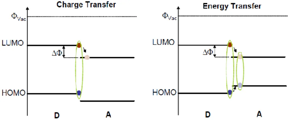
The most important discovery on the route to high efficiency organic solar cells was in 1986, when Tang[8] discovered that much higher efficiencies (about 1%) can be attained when two organic materials, an electron donor (D, p-type) and an electron acceptor (A, n-type), are brought together (heterojunction) in one cell[8,40-42]. The idea behind a heterojunction is to use two materials with different electron affinities and ionization potentials. Using this approach, photo-generated excitons in the organic layer can be efficiently dissociated into free carriers at the interface, whereas in single-layer devices most excitons recombine after a short time. The charge separation occurs at the interface between donor and acceptor molecules, where the resulting potential drop is strong enough to favor exciton dissociation.
After photo-excitation of an electron from the HOMO to the LUMO, the electron can jump from the LUMO of the donor (the material with the higher LUMO) to the LUMO of the acceptor if the difference ΔΦ between the ionization potential of the donor and the electron affinity of the acceptor is larger than the exciton binding energy (see fig. 4). However, this process, which is called photo-induced charge transfer, can lead to free charges only if the hole remains on the donor due to its higher HOMO level. In contrast, if the HOMO of the acceptor is higher, the exciton transfers itself completely (energy transfer) to the material of lower band gap, accompanied by energy loss.
Figure 4 - The heterojunction interface between two different semiconducting polymers (D=donor, A=acceptor): (left) “charge transfer”, by splitting the exciton; (right) “energy transfer”, by transferring the whole exciton from donor to acceptor.
For efficient exciton dissociation at the heterojunction, the donor and acceptor materials have to be in close proximity. The optimum length-scale is in the range of the exciton diffusion length. On the other hand, the thickness of the active layer should be comparable to the penetration length of the incident light, which is typically 80–200nm for organic semiconductors.
In the effort to develop viable organic photo-voltaic devices, this heterojunction concept has been applied in two different ways: the donor–acceptor planar organic semiconductor cell (double- or bi-layer)[8,15,42-45], and the bulk-heterojunction (BHJ) layer solar cell[7,40,41,46,47] (fig. 5).
Figure 5 - The fundamental physical processes in a heterojunction device: a) double-layer, b) bulk-heterojunction. The dashed line represents the energy levels of the acceptor, while the full lines indicate the energy level of the donor in the device. Sunlight photons which are absorbed inside the device excite the donor (1), leading to the creation of excitons in the conjugated polymer. The created excitons start to diffuse (3) within the donor phase and, if they encounter the interface with the acceptor, then a fast dissociation takes place (4), leading to charge separation. The resulting metastable electron–hole pairs across the D/A interface may still be Coulombically bound and an electric field is needed to separate them into free charges. Therefore, at typical operation conditions, the photon-to-free-electron conversion efficiency is not maximal. Subsequently, the separated free electrons (holes) are transported (5) with the aid of the internal electric field, caused by the use of electrodes with different work functions, towards the cathode (anode), where they are collected (6), and driven into the external circuit. However, the excitons can decay (2) if they are generated too far from the interface. Thus, the excitons should be formed within the diffusion length of the interface.
1.2.1 - Double-layer
Basically, the bi-layer device consists of two different organic layers, deposited sequentially, between two electrodes. This geometry guarantees directional photo-induced charge transfer across the interface. Since both types of charge carriers travel to
losses are significantly reduced. Commonly, this device structure is applied to organic solar cells made with small-molecules (very-low molecular weight organic materials), deposited via vacuum techniques[48]. Polymers, large molecule (macromolecule) composed of repeating structural units typically connected by covalent chemical bonds (π-conjugated polymers), can also be used for realize such bi-layer structure[49-51]
; however, the polymers have to be dissolved in solution, so the deposition of the polymer for the second layer can damage the lower one, resulting in a faulty device (the so-called solvent-crossing problem).
The organic D/A interface separates excitons much more efficient than an organic/metal interface in the single layer device. If the excitons are generated in close proximity to an interface, they have high chance to be separated into free charge carriers, which may diffuse or drift to the corresponding electrodes. However, because the individual layer thicknesses are larger than the exciton diffusion length, most excitons will decay (fig. 6). Therefore, the width of an effective light-harvesting layer depends by two opposite parameters, absorption depth of the film and exciton diffusion length, limiting indeed the efficiency of the planar structure.
Figure 6 - Principle of charge separation in double-layer organic heterojunction solar cells.
1.2.2 - Bulk-Heterojunction
A revolutionary development in OPVDs came in the mid 1990s with the introduction of the dispersive (bulk-) heterojunction, where the donor and acceptor materials are blended together. In the ideal case, a bulk-heterojunction (BHJ) layer is a bi-continuous composite of donor and acceptor phases, thereby maximizing the
of the same order of the exciton diffusion one. The exciton decay/recombination processes result dramatically reduced, since in the proximity of every generated exciton there is an interface with an acceptor, where fast dissociation takes place. Hence, charge generation ensues everywhere in the active layer. Provided that continuous pathways exist for both materials (D and A) from the interface to the respective electrodes, photon-to-electron conversion efficiency and photo-sensitivity is dramatically increased (with respect of bi-layer structure).
Generally BHJ devices are prepared using conjugated polymers as organic materials; in fact, layers containing a mixture of an electron donating and an electron accepting polymer, (so-called polymer blend), can be prepared by deposition of a solution containing both polymers dispersed in the same solvent[40,47,52]. Since the entropy of mixing is generally low for polymers, solid polymer blends tend to phase-separate, leading to a distributed bulk-heterojunction. A large donor-acceptor interface is formed without any additional processing steps. If donor and acceptor components are intimately mixed such that the length-scale of the phase separation is in the range of the exciton diffusion length (<10nm), nearly all excitons can be separated. Moreover, when a thin layer of immiscible polymers is deposited from solution, the resulting morphology strongly depends on various parameters, such as the individual solubility of the polymers in the solvent, the interaction with the substrate surface, the layer thickness, the deposition method and the drying process[53-59]. Thus, the real advantage of these BHJ devices is the ability to deposit the composite active layer from solution in a single step, using a variety of techniques that range from ink-jet printing to spin-coating or casting.
1.2.3 - Fullerene derivatives as organic acceptor materials
Regardless of the method of preparation, one key feature of BHJ organic solar cells is the almost ubiquitous use of fullerenes (any molecule composed entirely of carbon; usually, they are carbon sphere C60, buckminster-fullerenes) as the
electron-accepting component. The high electron affinity and superior ability to transport charge make fullerenes the best acceptor component currently available for BHJ devices.
Fullerenes are currently considered to be the ideal acceptors for organic solar cells for several reasons. First, they have an energetically deep-lying LUMO[60], which endows the molecule with a very high electron affinity relative to the numerous potential organic donors. Luminescence quenching[61] and ultrafast photo-induced
(as acceptor) had already been observed in 1992. The triply degenerate LUMO of C60
also allows the molecule to be reversibly reduced with up to six electrons, thus illustrating its ability to stabilize negative charge. Importantly, a number of polymer– fullerene blends are known to exhibit ultrafast photo-induced charge transfer (~45fs), with a back transfer that is orders of magnitude slower[63]. Furthermore, C60 has been
shown to have a very high electron mobility, up to 1cm2/V·s in field-effect transistors (FETs)[64]. These fundamental properties, coupled with the ability of fullerene
derivatives (C60 sphere functionalized with a chemical tail to render them soluble, see
fig. Figure 7) of packing effectively in crystalline structures favorable to charge transport[65], have made fullerenes the most important acceptor materials for BHJ solar cells. The electronic structure of the fullerenes can be considered to be constant regardless of the chemical functionalization used for solubilization: for most fullerene derivatives, the first reduction potential only varies by ±100mV relative to C60[66-68].
1.3 - Active layer
1.3.1 - P3HT:PCBM blendNowadays, among the organic materials investigated for BHJ-layer organic solar cells, the most effective polymer–fullerene combination is the P3HT:[60]PCBM system, as independently reported from many different research groups, reaching efficiencies close to 5%[17,19,20,69–71]. Conjugated polymer P3HT, poly(3-hexylthiophene), has been studied intensively due to its excellent hole mobility (P3HT is used as channel material in OTFTs) and optical absorption (absorbs photons with wavelengths smaller than 675nm, having Egap~1.85eV), while [60]PCBM, [6,6]-phenyl-C61-butyric acid methyl
ester (frequently is mentioned simply PCBM, as done in the rest of this work), is the
most used fullerene derivative, because of its high electron mobility (close to pure C60)
and solubility in many standard solvents employed for conjugated polymers, as toluene, xylene, (di)-chlorobenzene, chloroform.
Figure 8 – State-of-the-art blend organic materials for BHJ solar cells, P3HT (donor polymer) and [60]PCBM (acceptor fullerene derivative).
1.3.2 - Morphology
Although the electronic relationship between P3HT and PCBM is certainly favorable, the performance of devices still depends on the physical interaction of the donor and acceptor components, which is manifested by the composite morphology. It is ultimately the morphology of the active layer (and the ability to control it) that has led to the best performance in this type of BHJ solar cells. Several levels of optimization have been employed in the most efficient versions of the P3HT:PCBM solar cells.
1.3.3 - Weight ratio (X:Y)
The first parameter in the control of layer morphology is the amount of one material with respect of the other one (weight ratio, generally referred to the polymer). In the case of P3HT:PCBM, both (1:1)[20] and (1:0.8)[17,19] w.r. of polymer to fullerene was found to be optimal. However, several reports indicate that ratios as low as (1:0.6) or (1:0.43) also lead to optimized performance[69,72]; later in this work, it will be showed a device performance of ~5% with a w.r. of (1:0.7). These results point to a good inherent miscibility between P3HT and PCBM.
1.3.4 - Solvents
Directly linked to weight ratio (and relative morphology) is also the choice of solvent for the blend solution. It depends on materials solubility and solid content (weight percentage of solute in solvent), and could be revised according to solution-techniques used for layer deposition (basically spin-coating). Chlorobenzene is generally used as solvent[17,19], because both P3HT and PCBM are soluble, although
ortho-dichlorobenzene has been reported to give devices with comparable
performances[20,73].
1.3.5 - Annealing treatments
Among the best works reported so far, the most representative of the morphology impact in P3HT:PCBM device performance is of Ma et al[19] (fig. 10d). They have blended in chlorobenzene 10mg/ml of P3HT and 8mg/ml of PCBM; after spin-coating, a relatively homogenous composite film is formed in which little or no-phase segregation is observed beyond the length scale of a few nanometers. Such untreated films were observed to give energy conversion efficiencies less than 1% under AM1.5G conditions[74], with respect of the same film after thermal treatment. It suggests that the kinetically trapped morphology initially obtained is unstable to phase segregation, being driven by the strong tendency of the two components to crystallize independently. The judicious application of an external variable, such as heat or solvent vapour, can drive phase segregation of P3HT and PCBM into bi-continuous domains.
1.3.6 - Thermal annealing
A variety of methods have been used to optimize the morphology of these films to obtain the best solar cell performance. The most commonly used technique involves thermal annealing, as first reported by Padinger et al.[75]. Heating the active layer of the device to a temperature greater than the glass-transition temperature Tg of P3HT (the Tg
value of P3HT has been reported to be between 110°-125°C[73,76]) allows the polymer chains to reorganize and the fullerene molecules to freely diffuse into the composite and reorder in a more thermodynamically favorable way (fig. Figure 9).
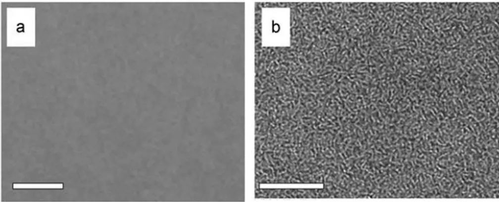
Figure 9 - TEM images of a P3HT:PCBM composites: a) blend (1:1) of P3HT and PCBM prior to annealing (scale bar 0.5mm); b) the same sample after annealing at 150°C for 30min (scale bar 0.5mm).
X-Ray investigations allowed the development of a microscopic picture of the annealing process[77] (fig. 10a/b/c). Several detailed morphological studies revealed that the organization of the P3HT:PCBM is modified upon annealing[19,78], with fibrillar-like P3HT crystals embedded in a matrix believed to comprise mostly PCBM nano-crystals and amorphous P3HT[79]. Since P3HT crystallizes faster and more readily than PCBM, the growth of crystalline P3HT domains upon thermal treatment is accompanied by free diffusion of the fullerene molecules within the composite film, thus leading to aggregation of PCBM in domains that crystallize slowly. A bi-continuous network with nanometer-scale phase segregation is obtained by judicious application of this thermal annealing step, in which the heating time and temperature is carefully controlled. The ability to control the domain size at short annealing times is attributed to inhibition of the fast diffusion of PCBM by the rapidly formed P3HT fibril network acting as boundaries and enforcing a measure of control over the degree of phase segregation. Once a highly ordered bi-continuous network of P3HT and PCBM has been induced by thermal-annealing, device efficiencies can jump to ~5%.
However, some questions still remain about how this treatment has to be used. Annealing temperatures between 100°-150°C are applied for as little as 1min or up to 2h, obtaining similar results. Also, another critical point to mention is that thermal annealing prior to deposition of the metal cathode (generally aluminum) usually results in poorer device performance than when annealing is performed after deposition of the cathode[80-82].
Anyway, upon annealing, all electrical parameters of the device are altered: the VOC was usually found to decrease slightly, while both ISC and FF increased
significantly. Figure 10d/e illustrates a typical enhancement of efficiency η[19] and of external quantum efficiency (EQE)[79] upon thermal annealing. This phenomenon is attributed mainly to an enhancement of the charge-carrier transport, a larger hole mobility[78,83], and reduced both wastefulness[84] and recombination kinetics[85,86].
Figure 10 - (a/b) Schematic pictures showing the microscopic process during annealing; (c) XRD spectrum on a P3HT:PCBM blend before and after annealing, showing the evolution of the a-axis oriented P3HT crystals[77]; (d) current–voltage curve for a P3HT:PCBM solar cell prior to annealing (, η=0.82%), after annealing at 70°C for 30min (Δ, η=3.2 %), and 150°C for 30min (■, η=5%)[19]; (e) EQE spectrum for a P3HT:PCBM composite solar cell before (▲) and after thermal-annealing (●) [62].
1.3.7 - Solvent annealing
Similar improvements in device efficiency can be observed with other techniques such as solvent-annealing or the controlled evaporation of solvent from the deposited films (slow-process). Yang et al. have pioneered the use of controlled solvent evaporation during film formation in P3HT:PCBM solar cells[20,87]. It is observed that, when films of P3HT:PCBM (1:1) blend are spin-coated from a ortho-dichlorobenzene solution, the rate of solvent evaporation prior to deposition of the cathode has a strong effect on the performance of the device. When the cast film is allowed to dry in a covered petri-dish over 20min prior to Al (aluminum) deposition, an energy conversion efficiency of 3.52% is measured without thermal annealing treatment. If the same film is dried in a nitrogen flow for 3min, the maximum energy conversion efficiency is reduced to 2.80%, while acceleration of the rate of solvent evaporation by heating the substrate to 50°-70°C leads to further efficiency reductions to 2.10 and 1.36%, respectively. This experiment suggests that both the presence and residence time of solvent molecules in the film contribute to phase reorganization, and leads to results that are roughly similar to those obtained by thermal annealing.
Further experiments showed that the best device (3.52%) obtained by solvent-evaporation benefited from subsequent thermal annealing at 110°C for 10min, increasing its efficiency up to 4.37%. This finding suggests that either the evaporation time of 20min was insufficient to allow optimal reorganization of the morphology, or that thermal annealing provides a more effective driving force for reorganization of the film. A matching between the two annealing process can have a key role for further enhancement in P3HT:PCBM solar cell performance.
Figure 11 - Effect of growth rate on the morphology of a P3HT:PCBM (1:1) active layer. AFM phase image of (a) fast grown and (b) slow grown polymer-fullerene blend films for a 1×1μm2 surface area[87].
Figure 12 - Effect of film growth rate on EQE of P3HT:PCBM (1:1) solar cells. EQE measurements are plotted for two types of active layer: slow-grown (no. 1) and fast-grown (no. 7). The efficiency maximum for slow-grown film is ∼63%, which is more than three times that of fast-grown film (∼19%)[20].
1.3.8 - Mobility
Such performance disparity between annealed and untreated devices is directly related to differences in the mobility of the charge carriers in the active layers. In fact, the mobilities of organic semiconductors are several orders of magnitude less than of inorganic ones[88], due to transport processes subjected to hopping transport (molecule-to-molecule transfer of carriers) in contrast to the band transport. Therefore, thanks to annealing, a more favorable reorganization of P3HT takes place, leading to a higher mobility for both holes and electrons (specially for hole mobility, with an increase by a factor that can reach a value of ~45[89]).
1.3.9 - Layer thickness
All of these results emphasize the importance of an annealing step for reorganizing the polymer chains to achieve maximum mobility of the charge carriers; the higher mobility allowed a thicker film to be used, which resulted in an increased photo-current as an effect of increased absorption. However, also the film thickness influences the annealing conditions used, and so the mobility achieved by active layer. Li et al.[81] reported that their best performance (4%) in blends (1:1) of P3HT and PCBM is achieved with 63-nm-thick films, which are thermally annealed at 110°C for 10min, whereas the use of 155-nm-thick films under the same conditions led to efficiencies of only ~2%.
The unbalanced effect of annealing at different layer thicknesses could be addressed to a trade-off between the enhancement of light absorption (for thicker layers) and the increased length of carrier pathways to electrodes (thicker layers lead to major recombination losses).
However, it is not completely true. Dennler et al.[90] predicted with theoretical calculations the number of photons (Nph) absorbed in a P3HT:PCBM layer versus its
thickness for an organic solar cell (fig. 14). In a real device, the absorption in the photoactive blend cannot be 100%, because the active layer is embedded within a stack of several layers, which have different complex refractive indexes. Thus, absorption can occur in some layer located between the incident medium and the active layer, and reflection can happen at any interface located before the bulk of the active layer. It appears that Nph generally increases with increasing thickness, but not monotonically. If
the thickness of the layers is smaller than the coherence of the light, interference occurs, because the light is reflected by the opaque electrode. Assuming an active layer that has a thickness of 400nm, the maximum JSC, with an average internal quantum efficiency
(IQE) of 100%, is 12.8 mA/cm2. If the average IQE is lower than 100%, JSC is reduced.
At 80% average IQE, JSC should be around 10.2mA/cm2. Thus, despite the fact that the
theoretical short-circuit current density of a P3HT:PCBM blend could be close to 19mA/cm2[90], the practically achievable JSC of real devices will be in the range of
10–12mA/cm2. Thus, several layers suffer differently the same treatment conditions also because the thickness-dependence of light absorption is not linear.
Figure 14 - Number of photons (Nph) absorbed in the active layer (AL) under AM1.5G, calculated
for a device having the following structure: glass/ITO/PEDOT:PSS/P3HT:PCBM(xnm)/Al. The right axis represents the corresponding short-circuit current density JSC at various IQE[90].
1.3.10 - Influence of molecular weight and regio-regularity
Like in inorganic semiconductors, where the material has to be of very high purity in order to realize good devices, also in conjugated polymers it is required some intrinsic features that influence the solar cell performance. Particularly for P3HT, they are the molecular weight (MW, the weight of a polymer chain) and the regio-regularity
(RR, defined as the percentage of monomers adopting a head-to-tail configuration, rather than a head-to-head).
The influences of the MW on the performance of P3HT:PCBM was quickly
addressed once the annealing process was understood[91]. Too-short molecular-weight fractions were shown to have inferior mobility, most likely because of main-chain defects and low mobility[92-94]. Furthermore, the role of smaller MW fractions was found
to initiate or facilitate the growth of crystalline fibrils during the annealing step, leading to a large number of small crystals, while higher MW P3HT stays amorphous[92-94]. On
the other hand, too-high molecular weights produced highly entangled polymer networks, rendering annealing either impossible or requiring higher temperatures and/or longer annealing times[95]. The ideal morphology appears to be formed for P3HT with an average-MW in the range 30.000–70.000 (~50.000), and a rather high polydispersity
of around 2, which gives a good mix of highly crystalline regions formed by low-MW
P3HT embedded in and interconnected by a high-MW P3HT matrix[96].
Also the effect of the polymer‟s regio-regularity is critical. A specific threshold (RR≥95%) seems to be necessary to give the highest JSC and FF[97], mainly because of
the better transport properties of highly RR-P3HT[98].
1.4 - Breaking the η≈5%
P3HT:PCBM solar cell seems to achieve its performance limit at ~5%. The photon flux reaching the surface of the earth from the sun occurs at a maximum of approximately 1.8eV (~700nm); however, P3HT (Egap~1.9eV) doesn‟t harvest
effectively photons from the solar spectrum. It is calculated that P3HT is only capable of absorbing about 46% of the available solar photons[99], and only in the wavelength range of 350-650nm. The limitation in the absorption is primarily due to limited spectral breadth rather than the absorption coefficient (typically in conjugated polymers it is extremely high, on the order of 105/cm[100]).
1.4.1 - Ideal donor polymer
However, one of the best features of organic polymers is the chance to tailor their electrical/optical properties, and this is the best strategy for arise further the performance of BHJ devices. Developing a polymer that could capture all of the solar photons down to 1.1eV would allow absorption of 77% of all the solar photons[63]. Expanding the spectral broadness of absorption in polymer–fullerene composites has most commonly been pursued by extending (or shifting) the polymer absorption spectrum into the near-infrared region. While low-bandgap polymers have often been
absorption is not sufficient to harvest more solar photons. What is needed is to extend the overlap with the solar spectrum to gain broader coverage, while also retaining high absorption coefficients at relevant wavelengths and suitable energy levels for interaction with PCBM.
As mentioned before, considering a fullerene derivative (PCBM) as the perfect acceptor (in terms of electrical characteristics, as electron mobility and HOMO-LUMO levels), the first constraint is that the polymer donor must be capable of transferring charge to the fullerene upon excitation. A energetic driving force, exceeding the exciton binding energy (up to ~0.5eV[101]), is necessary for this process to be favorable. Empirically, the overall energetic driving force for a forward electron transfer from the donor to the acceptor is represented by the energy difference (offset) between the LUMOs of the donor and acceptor, and a minimum energy difference of 0.3eV is required to affect the exciton splitting and charge dissociation[102,103]. Furthermore, an energy difference between the LUMOs larger than this minimum value does not seem to be advantageous, and indeed results in wasted energy that does not contribute to the device performance[104]. The LUMO of an ideal polymer would have a minimum energy difference with the LUMO of acceptor; in this way, wasted energy upon exciton splitting would be avoided and the bandgap of the polymer would be minimized, so as to maximize the absorption of light. Thus, the LUMO of an ideal polymer would reside at approximately 3.9eV, since for PCBM the energy LUMO is about 4.2eV (fig. 16).
The HOMO energy of the ideal donor polymer would then be determined by considering the bandgap of the polymer, and hence the absorption of light, as well as the influence on the open-circuit voltage (see fig. 17). The lower is the energy of the HOMO, the greater is the maximum value theoretically attainable for VOC, but, at the
same time, the larger the bandgap, the poorer the spectral overlap with the photon flux from the sun. A compromise is found by considering that a bandgap of about 1.5eV is an optimal value for a polymer absorber[99]. This value gives a HOMO energy of about 5.4eV, which corresponds to a maximum attainable VOC value of 1.2V. The optimal
bandgap value of 1.5eV has been determined through a detailed analysis that balances the achievable VOC value and the donor bandgap[105]. A broad absorption band for the
polymer between 4.1-1.5eV and a high absorption coefficient (at least 105/cm) are also assumed to be a mean criterion for an ideal system. A high charge carrier mobility for the polymer, commensurate with that of PCBM, 10-3cm2/V·s measured in a SCL (space–charge limited) regime[106], or 10-1cm2/V·s measured in FETs[107], is also assumed for an ideal donor. At both an EQE and a FF of 65%, such a polymer could reach practically power conversion efficiencies over 10%[105].
1.4.2 - Ideal acceptor fullerene derivative
On the contrary, someone can develop new acceptor fullerene derivatives for better device performance. PCBM[108] was first reported in solar-cell applications in 1995[40], and since then no significant better acceptor has been found.
The ideal acceptor material for a bulk-heterojunction solar cell should have a strong absorption profile complementary to the donor one. Furthermore, the offset of donor/acceptor LUMO levels needs to be optimized, to ensure efficient charge transfer and a high open-circuit voltage at the same time. Finally, the acceptor needs to exhibit sufficient electron mobility in composites with the donor. So far, only derivatives of C60
and C70 have been reported to give highly efficient BHJ-SCs, despite the fact that the
position of the HOMO and LUMO levels and the optical absorption are not ideal for most of the donor polymers[105]. It is the shift of the acceptor LUMO level that can give the biggest boost in efficiency. In the case of P3HT:PCBM blends, the acceptor level offset is ~1eV. Thus, more than 50% of the available energy, after photo-excitation, is lost. A reduction of the LUMO offset would be directly translated in an increased open-circuit voltage (see fig. 16). A novel acceptor with a ~600mV higher-lying LUMO level, compared with PCBM, could theoretically double the efficiency of P3HT-based bulk-heterojunction solar cells.
Recently, Yamanari et al.[109] have showed the better performance of solar cells made with P3HT blended with [70]PCBM. Although the reported enhancement is still low, however these studies didn‟t examine accurately the best annealing parameters for the morphology of this blend, so a major increase in device performance is still possible.
1.4.3 - Additives
Additives were reported as an alternative method to create better order in blends of P3HT and PCBM. Oleic acids[110] and alkylthiols of different lengths[111], like
n-hexylthiol, n-octylthiol, or n-dodecylthiol, were added to P3HT:PCBM solutions, and
allowed the formation of thin films with slightly enhanced hole mobility and significantly enhanced charge-carrier lifetimes, because of enlarged P3HT domains with higher crystallinity. Nevertheless, some thermal annealing was still necessary to give the highest possible performance. Another, quite similar approach to control the nanomorphology of P3HT:PCBM blends requires the addition of „non-solvents‟ into the
the polymer into nano-particulates, similar to the mini-emulsion mentioned above. Addition of nitrobenzene (NtB) to a P3HT:PCBM solution in chlorobenzene allows an increase in the volume fraction of P3HT aggregates from some 60% to up to 100% with increasing NtB content. Photovoltaic devices from P3HT:PCBM mixtures with NtB as additive allowed the manufacture of devices with efficiencies as high as 4% without thermal annealing. These experiments proved that a good part of the thin film morphology can already be introduced on the solution level.
Figure 18 - UV-Vis absorption spectra of P3HT:PCBM (3:2) as-cast PV devices with 0% (solid line), 0.33% (dashed line), 0.67% (dotted line), 1.6% (dashed–dotted line), 3.2% (short-dashed line), and 6.3% (solid line) nitrobenzene added into the chlorobenzene solvent. Offset from the other spectra is the as-cast PV device from the ortho-xylene dispersion (triangles)[132].
Recently, several research groups, directly related to Konarka[114] and Solarmer[115], at the moment world leader companies for polymer photo-voltaics, have broken the 5% limit for efficiency, thanks to the application of both additives and new low-bandgap donor polymers (fig. 19).
Figure 19 – UV-Visible absorption spectra of new donor polymers. (a) PCPDTBT:[70]PCBM films, processed with 1,8-octanedithiol: (black) before removal of [70]PCBM with alkanedithiol; (red) after removal of [70]PCBM with alkanedithiol; (green) pristine PCPDTBT film[114]. (b) PTB7 pristine polymer film ( ) and PTB7:[70]PCBM blend film in (1:1.5) w.r. (●)[115].
1.4.4 - Tandem solar cells
Since it seems improbably that a single organic material can absorb efficiently from the blue to the infrared region, tandem structures were proposed, where different sub-cells absorb different wavelength regions. The tandem approach allows researchers to tackle two additional limitations intrinsic to π-conjugated molecules. The first one is the poor charge transport, which hinders the realization of a thick active layer that would absorb maximum light. The second relates to the very nature of light absorption in those materials, which yields an absorption spectrum made of discrete broad peaks rather than a continuum. Hence, a combination of various different materials can help to more efficiently cover the emission spectrum of the sun.
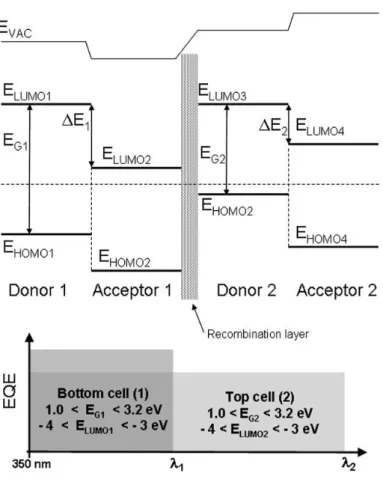
The series connection between the two devices is the critical technology limit for tandem solar cells. In many cases, thin (1–2 nm) layers of metal are used. This recombination layer appears necessary to induce the alignment of the quasi-Fermi level of the acceptor of one cell with the donor of the other one (see fig. 20).
Figure 20 - Simplified band diagram of tandem cells composed of two sub-cells connected in series by a recombination layer.
The highest-efficiency tandem devices reported up to date are entirely solution processed. These devices had a 38% performance increase versus the best single device[116], and an uncertified efficiency of 6.5% was reported (fig. 21). The intermediate layer comprised a TiOx sol–gel layer and a PEDOT:PSS layer; the bottom
cell was made of a blend of PCPDTBT and PCBM, and the top cell was based on a P3HT:[70]PCBM mixture. Noticeably, the selective usage of [60]PCBM or [70]PCBM allowed maximization of the number of photons absorbed in each sub-cell, because of a reduction of the overlap between the respective absorption spectrum of the active blends[117].
Figure 21 - Structure and I-V characteristics of the tandem cells realized with TiOx sol-gel
layer[116].
Although all the devices reviewed above are based on a two-terminal concept comprising cells connected in series, several groups followed other approaches. The optimization of semi-transparent top electrodes allows the superposition of two independent devices, and connects them either in series or in parallel[118].
However, the most innovative device architecture, which is also accounted for under tandem cells, is probably the folded-reflective tandem device[119] (fig. 22). This geometry has three major advantages. First of all, the reflected light of one cell is directed toward the second device, which ideally has a complementary absorption spectrum. Second, the tilting of each cell enlarges the light path within the active layer[120]. Finally, using an angle between the cells smaller than 90° can cause a light-trapping effect to occur, significantly enhancing the absorption, and hence the photo-generation, of charge carriers. In the case of solar cells with thin active layers (50–60nm) and rather low EQEs, an almost two-fold enhancement of the performance was reported for an angle of 40° between the cells. In the case of highly efficient single-junction cells, the V-shape geometry is only beneficial if semiconductors with two different bandgaps are operated.
Figure 22 - Sketch of the V-shape folded-reflective tandem solar cell[119].
1.5 - Stability of BHJ devices
A final concern of critical relevance to the optimization of polymer–fullerene BHJ-SCs is the stability of the device. Stability can be assessed in regard to a variety of different parameters, including ambient and thermal factors. While ambient stability may be realized through encapsulation to protect devices from the action of oxygen and water, thermal stability is a critical issue that currently plagues organic BHJ-SCs. Devices based on P3HT:PCBM show a good thermal stability because of the inherently great miscibility of the two components. The precise primary structure of the P3HT has been proposed to play a major role in the thermal stability of the composite[122,133]. At the moment, the use of compatibilizers and crosslinking[124,125] are the two general routes explored to improve the thermal stability and reduce phase separation in polymer–fullerene bulk-heterojunction solar cells.
C
HAPTER
2
R
EALIZATION AND
CHARACTERIZATION
The realization of polymer bulk-heterojunction solar cells was a research field totally new in our university. From this point of view, the primary aim of the work was to study and reproduce the state-of-the-art of polymer photo-voltaic devices, starting from scratch. Thus, first an intense literature research of both materials and techniques was performed, then the acquired knowledge was applied for the realization and characterization of the organic photo-voltaic devices.
The optical properties of the deposited film was studied by absorption spectra measurements, whereas the opto-electrical properties of the whole photo-voltaic device was investigated by external quantum efficiency (EQE) and I-V curves (under illumination).
2.1 - Experimental
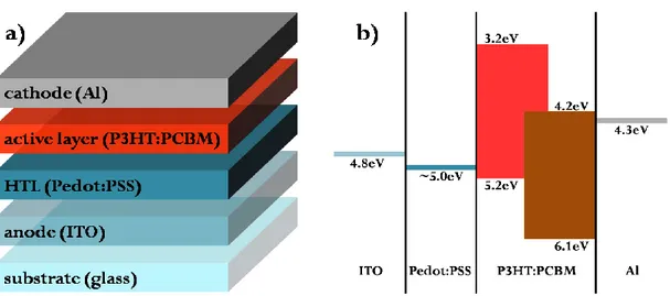
The best polymer bulk-heterojunction solar cell obtained was fabricated as follow (see fig. 23). For the active layer, the blend solution is prepared using P3HT:PCBM (1:0.7) in ortho-dichlorobenzene; the solid content is about 1% in weight. The device was realized on a glass substrate coated by a transparent conductive oxide layer of ITO (indium tin oxide, ΦITO≈4.8eV, ), working as
anode, previously cleaned with acetone and isopropanol in ultrasonic-bath (10min each solvent-step). First, a layer of poly(3,4-ethylenedioxythiophene):poly(styrene-sulfonate) (Pedot:PSS, Clevios P, VP AI 4083) is deposited by spin-coating from aqueous dispersion at 2000rpm for 60sec, subsequently heated on a hot-plate at 150°C for 10min (final thickness of ~80nm). Then, the P3HT:PCBM (RR-P3HT 95%, Rieke Metals, 4002-EE; [60]PCBM, Solenne BV, 99%) layer is deposited at 400rpm for 60sec; the solvent remaining on top of the layer is allowed to exhale for 2h. The final thickness is about 80nm (fig. 24). Finally, an aluminum electrode of ~100nm is evaporated in high-vacuum (~2·10-6mbar) at 1.0Å/sec. After evaporation, the device is thermal annealed on hot-plate at 150°C for 10min. The whole device was processed inside a glove-box in nitrogen inert atmosphere (fig. 25).
Figure 24 – Profilometer measures of (a) Pedot:PSS and (b) P3HT:PCBM layer thickness.
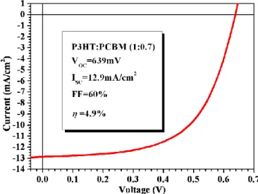
In figure 26 the I-V behaviour is showed. Under AM1.5G illumination of 100mW/cm2 (1sun), the polymeric solar cell has an open-circuit voltage of 639mV, and a short-circuit density current of 12.9mA/cm2; even with such high current, the efficiency reaches only 4.9%, because of the limited fill-factor (~60%). However, this performance is very close to the state-of-the-art of ~5%[17,19,20,69-71].
Figure 26 – I-V curve of the best P3HT:PCBM solar cell under 1sun of illumination.
A compare of optical and opto-electrical properties is accomplished (fig. 27). Although a major absorbance of active layer doesn‟t mean necessary a higher efficiency (a thicker layer could absorb better having worse charge carrier conductivities), in this case they match perfectly. The mean peak of absorption spectrum is at λmax=513nm, and
the same for maximum EQE (~50%). In addition, also secondary peaks near 560 and 600nm exhibit counterchecks.
2.2 - Patterning of electrodes
To characterize properly the performance of an organic photo-voltaic device as solar cell, it is necessary to know correctly the active area, that results from the vertical overlap of anode and cathode. Thus, it is extremely important to control the patterning of both electrodes.
Our devices have an active area of 25mm2 (5×5mm2), obtained with the 90° superposition of strip-shaped electrodes, both large 5mm (see fig. 28). Thanks to this fabrication trick, is also possible to obtain 4 different devices (electrically isolated one from another) from the same substrate sample (2.5×2.5cm2).
Figure 28 – Realization of patterned devices.
2.2.1 - Wet-etching
The glass substrate used for device fabrication is completely covered by ITO. To obtain a selected removal of this layer (fig. 29), wet-etching technique (acid corrosion of bare oxide) is chosen. This method involves materials resistant to acid attack, that can be deposited on the oxide layer with the desired pattern, obtaining a selective removal of oxide after acid-bath.
Initially, a photo-resist polymer was chosen as warding material. It is spin-coated on the sample, then with UV light-source and shadow-mask (pattern printed on transparent sheet, see fig. 30) it is hardened only if directly exposed to UV radiation (photo-lithography approach). However, manual alignment of mask on sample was too difficult, and the resolution of such printed masks too low to produce a well-defined pattern for anode.
Figure 30 – Shadow-masks printed on transparent sheet for photolithography.
Afterwards, grip-tapes were adopted as guarding materials (3M white scotch). The sample is entirely covered with tape, then the pattern is engraved on it with CO2
laser-cutter (remote-controlled by PC, as a printer; see fig. 31a); the pattern is designed with dedicated software tools (CorelDraw X4), obtaining a well aligned and defined pattern (fig. 31b/c/d).
Figure 31 – ITO patterning steps: (b) tape coverage; (c) pattern design with laser; (d) sample prepared for wet-etching; (e) final pattern. (a) CO laser-cutter.
Regardless of pattern-designing method, subsequently the sample is dipped in acid-bath. Two different acids were tested, a mixture of HCl-HNO3 (hydrochloric-nitric
acid) (1:1) and HBr (hydrobromic acid). The first one was too much corrosive, even at
room temperature and diluted with water, HCl-HNO3-H2O (1:1:6), and the resulting
process was absolutely unmanageable (less then 2min to remove completely ITO from glass substrate; leaving over the sample in the acid-bath results in corrosion of lateral side of protected ITO). Instead, wet-etching with HBr ensues more controllable, since corrosive effect starts only heating the bath itself (on a hot-plate at ~60/70°C, fig. 32), and the ITO is completely removed only after 5/6min. Furthermore, HCl-HNO3 has to
be prepared on the occasion of use (disposable), whereas HBr can be used several times before discarding it.
Figure 32 – Glass beaker with HBr on a hot-plate for wet-etching treatment of ITO substrate.
2.2.2 - Laser-scribing
Although wet-etching is the best solution found for ITO anode patterning, another technique involving the use of laser-cutter (laser-scribing) was studied. Practically, the CO2 laser, with proper settings of power, focus and passage-speed, can
melt thin lines across the ITO layer, isolating electrically one side from another. Thus, with the appropriate design, it is possible to obtain an equivalent pattern of the wet-etching method (fig. 33).
Figure 33 – (left) Pattern design for laser-scribing; (right) laser-scribed ITO sample.
This alternative method of patterning was first applied because another transparent conductive oxide under study, FTO (fluorine-doped tin oxide), was affected not at all by acid-bath procedure. Then, it was tested also on ITO substrate. Figure 34 shows a comparison of the I-V behaviours of two devices made with the same process, with the exception of ITO patterning method. The results confirm that wet-etching still remains the best choice in terms of device performance, but also laser-scribing has its advantageous application, in particular because of its rapidity (only laser-cutter stage, one-step process instead of two).
2.2.3 - Evaporation
For the realization of patterned cathode, plastic shadow-masks are used (fig. 35). These masks are cut through laser, with a dimension of 26,5×26,5mm2, that matches the evaporator plate sample-holder (see appendix for details). The two strips are distant 2mm, as in the anode. The masks are made with flexible plastic, to ensure polymer layer safety during the load of samples inside the holders.
Figure 35 - Plastic shadow-mask used for aluminium evaporation.
2.3 - Hole transporting layer
Pedot:PSS is a polymer mixture of two ionomers, a sulfonated polystyrene, that can carry a negative charge, and poly-Edot, a conjugated polymer based on
polythiophene, carrying positive charges. Together, the charged molecules form a
macromolecular salt, dissolved in polar solvents, usually H2O (fig. 36).
This conductive polymer has many properties, useful if applied in organic solar cells. First of all, a Pedot:PSS thin film is a good hole transporting layer (HTL), as argued by its use in OLEDs or OTFTs fabrication[126]. Particularly for P3HT:PCBM solar cells, this feature, together with a favorable work function between ~4.9-5.2eV (depending on formulation), that matches the HOMO level of P3HT, makes Pedot:PSS layer an optimal hole collector, warranting a better performance of devices. Actually, in these organic devices, even if the working anode still remains the TCO layer, it is the Pedot:PSS thin film that operates energetically as “anode”; indeed, some research groups have realized polymer solar cells without TCO layer, using Pedot:PSS as working anode[127,128]. Furthermore, Pedot:PSS planes the roughness of ITO; this smoothening effect makes the active layer deposition more uniform (fig. 37).
Figure 37 - Smoothening effect of Pedot:PSS on ITO[126].
Pedot:PSS is dissolved in water, and active layer degrades if in contact with oxygen molecules (moisture in general). Thus, it becomes necessary to heat the sample, in order to dry out all the solvent. Furthermore, it is known that Pedot:PSS conductivity depends also from heating conditions (both temperature and treatment endurance)[129]. In figure 38 it is showed the dependence of device performance with respect of temperatures of heating treatment (100°, 120° and 150°C for 10min each one); as expected, the increase of temperature raises the conductivity of Pedot:PSS thin film.
Figure 38 – P3HT:PCBM solar cell performance at different heating temperatures of Pedot:PSS.
2.4 - Active layer
As said before, the performance of a polymer solar cell depends closely on active layer and its parameters (morphology, thickness); the phase separation of donor and acceptor materials has to be well-balanced between exciton dissociation and number of charge-carrier paths toward electrodes. Thus, it is extremely important to plan the preparation of the blend solution to attain the desired performance for device itself.
In order to prepare the solution, the solvent (oDCB) could be added directly to mixed solid content (P3HT and PCBM weighed together) in vial, and the mixture has to be stirred at least for 20h at 75°C, obtaining a complete dissolution of both two components. Alternatively, it is possible to dissolve single materials in solution (of the same solvent) with the same procedure, and blend the different solutions later (in this case, the mixed solution must be stirred at 75°C for 30min).
2.4.1 - Solid content
First aspect to ponder preparing blend solution is the solid content, that means the quantity of dissolved materials. According to it, the resulting mixture could be more or less appropriate for deposition purpose (depending on viscosity, purity and so on).
In figure 39 it is showed the dependence of device performance with respect of two different amounts of P3HT:PCBM solid content. The indicated percentage (1 or 2%) refers to solution weight in ortho-dichlorobenzene (1.307g/ml at 25°C); they corresponds to 13.2 and 26.5mg/ml, respectively. The 2% case has a minor efficiency, not only for a lower ISC, but more for a decrease of the FF. This worse performance is
consequence of a major viscosity of the deposited solution: on one hand, a major viscosity could be useful to obtain thicker and smoother films, on the other one, however, the solvent remains trapped more easily in the film, bringing to fewer charge-carrier paths.
2.4.2 - Weight ratio (X:Y)
The weight ratio (w.r.) is practically the fundamental variable in the quest for maximum performance of P3HT:PCBM (or any other polymeric components) solar cells, mostly because both optical and electrical properties depends directly from it. Since even in literature no one has established the best ratio, such a study was essential to reach the better performances.
The w.r. (1:0.7) shows an overall increase of the spectral absorbance of the active layer (fig. 40), with respect of (1:1). Regardless the enhancement due to a major quantity of P3HT (total solid content of solution remains unaltered), the spectrum presents a red-shift of the mean absorbance peak, plus the emerging of secondary peaks (appearances of P3HT crystallization obstructed by PCBM cluster formation), typical of a good mutual penetration of both organic components in the layer matrix. Thus, this layer could have also better charge-carrier paths.
Figure 40 – Effects of weight ratio and thermal annealing on P3HT:PCBM layer absorbance.
This effect could be noticed also in the I-V behaviors (fig. 41). Two devices were fabricated with the same process, apart from weight ratio. Even if VOC and ISC are
very close (products are almost equal), the (1:1) device is highly limited by its FF, yielding to a worse efficiency.
Figure 41 – Effect of weight ratio on P3HT:PCBM device performance.
However, it has to be underlined that device performance depends also on other realization parameters (especially annealing treatment); for this reason, many have reached the same high device performance (~5%) with different choices of the weight ratio.
2.4.3 - Thickness
This parameter results from the deposition technique used to realize devices. Thus, it doesn‟t bring directly a characterization of polymer solar cells, but it could be a reliable source of information in conjunction with other measures.
Figure 42 shows the dependence of spectral absorption with deposition speed during spin-coating. Because the absorption coefficient of a layer is related to its thickness, it is possible to infer such layer feature from this type of measurements. In this work, for a blend solution of P3HT:PCBM (1:0.7) at 1% in weight, an angular speed of 1000rpm corresponds to a layer thickness of ~35nm, whereas at 400rpm a ~80nm layer is obtained.
Figure 42 – Spectral absorption of P3HT:PCBM layers spin-coated at different angular speeds.
2.4.4 - Thermal annealing
The heating treatment of the P3HT:PCBM active layer is extremely important, in order to achieve the best performance from polymer organic solar cells. P3HT needs energy to crystallize inside the blend matrix, reaching higher carrier mobilities; in the same time, PCBM has to cluster, and requires energy too.
The effects of thermal annealing on thin films are clear (fig. 40): on a P3HT:PCBM (1:1) layer, annealing leads to an overall increase of absorption coefficient, red-shift of the entire spectrum, and formation of secondary peaks; for (1:0.7) film, it is observed only the absorption increase, but solely because the other properties are triggered by the w.r. of blend itself; nevertheless, the treatment enhances them too.
As above mentioned, thermal annealing could be used merely as the active layer treatment (with depicted results), or better to the whole device, because, acting on the morphology of the thin film, it can improve also the adhesion of the polymer layer with the evaporated cathode.


![Figure 8 – State-of-the-art blend organic materials for BHJ solar cells, P3HT (donor polymer) and [60]PCBM (acceptor fullerene derivative)](https://thumb-eu.123doks.com/thumbv2/123dokorg/7609966.115189/19.892.319.612.524.730/figure-state-organic-materials-polymer-acceptor-fullerene-derivative.webp)
![Figure 21 - Structure and I-V characteristics of the tandem cells realized with TiO x sol-gel layer[116]](https://thumb-eu.123doks.com/thumbv2/123dokorg/7609966.115189/34.892.175.761.130.356/figure-structure-characteristics-tandem-cells-realized-tio-layer.webp)