2D VERTICAL HETEROSTRUCTURES:
GROWTH, PROPERTIES AND APPLICATIONS
ANTONIO ROSSI
Advisor
Dr. Camilla Coletti
Supervisor
Prof. Giuseppe Carlo La Rocca
FOREWORD
This thesis is the result of my research activity at NEST laboratory of Scuola Normale Superiore in Pisa: I started my studies on two dimensional materials and their vertical heterostructure at the end of 2014. My interest in nanotechnologies applied to novel materials has matched with the research activity of the group I joined. This work was performed within a joint PhD program sponsored by Scuola Normale Superiore and Istituto Italiano di Tecnologia.
LIST OF ABBREVIATION 2d Two dimension 2DEG Two Dimension Electron Gas AFM Atomic Force Microscopy ALD Atomic Layer Deposition ARPES Angle Resolved Photoemission Spectroscopy BZ Brillouin Zone CB Conduction Band CESs Constant Energy Surface CLPES Core Level Photoelectron Spectroscopy CVD Chemical Vapor Deposition DFT Density Functional Theory DOS Density of State DS Doniach Sunjic EBL Electron Beam Lithography Ec Conduction Band Minimum EDCs Energy Distribution Curves EDX Energy Dispersive X-ray Spectroscopy Ef Fermi Energy EG Epitaxial Graphene Ev Valence Band Maximum FFT Fast Fourier Transform FOV Field of View FS Fermi Surface
FWHM Full Width Half Maximum h-BN Hexagonal Boron Nitride HPSI High Purity Semi-insulating HSQ Hydrogen Silsesquioxane IMFP Inelastic Mean Free Path LDOS Local Density Off States LEED Low Energy Electron Diffraction LEEM Low Energy Electron Microscopy LJ Lennard Jones LPE Liquid Phase Exfoliation MBE Molecular Beam Epitaxy MEM Mirror Mode MLG Monolayer graphene MOCVD Metal Organic Chemical Vapor Deposition MPI Max Plank Institute NEC Negative Electron Compressibility NEMS Nanoelectromechanical System PDMS Polydimethylsiloxane PES Photoelectron Spectroscopy PL Photoluminescence PPC Persistent Photocurrent QFMLG Quasi-Free Standing Monolayer Graphene RT Room Temperature
SPM Scanning Probe Microscopy STM Scanning Tunneling Microscopy STV Starting Voltage TFET Tunneling Field Effect Transistor TMDs Transition Metal Dichalcogenides tr-ARPES Time resolved ARPES UHV Ultrahigh Vacuum UPS UV Photoelectron Spectroscopy UV Ultraviolet VB Valence Band vdW Van der Waals vdWE Van der Waals Epitaxy vdWH Van der Waals Heterostructures XPEEM- X-Ray Photoemission Electron Microscopy XPS X-Ray Photoemission Spectroscopy µ-XPS Micro XPS PDOS Projected Density of States
CONTENTS
Introduction... i
Objective and results of the thesis ...ii
Thesis Outline ... v
Introduction to graphene, other 2d materials, and their
vertical heterostructures ...1
Graphene, a carbon honeycomb lattice... 1 Graphene properties and synthesis ... 2 Structure ... 2 Tight-binding approximation ... 4 Synthesis of Graphene... 8 Tungsten disulfide, Properties and synthesis ... 10 Structure ... 11 Electronic Properties ... 12 Synthesis of WS2 ... 15 Hexagonal Boron Nitride, Properties and Synthesis ... 18 Electronic Properties ... 19 Preparation of h-BN ... 19 2d vertical heterostructures ... 21Synthesis of 2d vertical heterostacks ... 23 Applications of vdwh ... 25 Tunneling devices for low-power electronics applications 26 Van der Waals Heterostructures for light detection ... 27
Experimental Techniques ... 29
Photoelectron Spectroscopy ... 29 Angle-Resolved Photoelectron Spectroscopy ... 34 Core Level PhotoElectron Spectroscopy ... 37 Low Energy Electron Diffraction ... 39 Low Energy Electron Microscopy ... 41 Nanospectroscopy @ Elettra ... 42 Atomic Force Microscopy ... 44 Scanning Tunnelling Microscopy ... 46 Raman Spectroscopy ... 47 Raman on Graphene and 2d materials ... 49 Photoluminescence ... 51 Transmission Electron Microscopy ... 52 Scanning Electron Microscopy ... 53 Energy-dispersive x-ray spectroscopy ... 54Graphene growth ... 55 Graphene from thermal decomposition of Silicon Carbide .... 56 Preparation of graphene on SiC (0001): experimental details 62 Graphene via CVD on metals. ... 64 Preparation of graphene on Cu foil: experimental details .. 66 Tungsten disulphide growth ... 67 Chemical Vapor Deposition ... 68 Process developed for the CVD synthesis of WS2 ... 70 Conclusions ... 81
Micro-structural, Electronic and chemical properties of
single-layer WS
2on epitaxial graphene on silicon carbide .... 83
Methods ... 85 experimental details ... 85 Core-level fitting procedure ... 87 Computational methods... 88 Results and discussion... 93 Structure and morphology ... 93 Electronic properties ... 95 Chemical properties ... 103Conclusions ... 106
Superlubricity of epitaxial monolayer WS
2on graphene
109
Superlubricity and TMD/graphene heterostacks: an overview ... 110 Experimental ... 111 Modeling and simulations ... 112 WS2 sliding on EG triggered by SPM tips ... 116 Modeling WS2 sliding trigger ... 122 Atomically resolved imaging of WS2 on graphene ... 125 Conclusions ... 127
Patterned WS
2/graphene heterostructures for efficient
multifunctional optoelectronic device ... 129
Methods. ... 130 Synthesis and patterned masking of graphene ... 130 WS2 synthesis ... 132 Device fabrication ... 132 Raman and photocurrent measurements ... 133 Results and discussion ... 134 Conclusions ... 145
Bilayer WS
2on graphene and h-BN: an all 2d platform for
valley-spintronics... 147
Methods ... 149 Bilayer WS2 growth ...149 Investigation techniques ...150 Results and discussion... 151atomic-thick WS2 on h-Bn: Strong light polarization conservation ...151
atomic-thick WS2 on CVD graphene: a possible platform for optical spin injection ...158
photo-emitting/photo-conductive patterns of WS2 on epitaxial graphene. ...161 Conclusions ... 164
Summary and perspective ... 165
Appendix A: ... 171
Methods ... 172 Results and discussion ... 172Appendix B: ... 175
Methods ... 175 Results and discussion ... 176 Conclusion ... 177Appedinx C ... 179
Methods ... 180 Results and discussion ... 182 Conclusions ... 187Bibliography ... 189
INTRODUCTION
Since its discovery, graphene has gathered increasing interest thanks to its outstanding properties such as astonishing carrier mobilities (up to 3,000,000 cm2/V s)1 and a thermal conductivity substantially higher than diamond (up to 5000 W/m K)2. In addition, it is practically transparent (it absorbs 2.3% of white light)3, it possesses an amazing impermeability to most gases and liquids4, unprecedented flexibility, mechanical strength and Young modulus5. What is truly outstanding is that these enticing properties are displayed by a real two-dimensional (2d) system, i.e., a honeycomb lattice of carbon atoms extending on a plane. Graphene is the first atomic-thick material to have been experimentally demonstrated and studied, but is not the only character in the world of 2d materials, which has been recently named Flatland6. Traditional layered materials such as transition metal dichalcogenides, hexagonal boron nitride, and black phosphorus can be isolated in their monolayer form, showing a number of interesting properties such as high spin-orbit coupling7, direct band gap8, charge density waves9, superconductivity10, and topological phases11. This plethora of 2d materials can be further expanded by arranging them together in vertical heterostructures. This allows for devising and implementing a new class of materials with potentially countless applications. Heterostructures are at the key of modern electronics. They have been at the center of semiconductors research for more than 50 years. Having materials with different properties combined together allows creating functional devices with non-trivial properties. The most common are covalent heterostructures, with chemical bonds between different layers12. However, combining materials with different lattice parameters creates defects, dislocations and even lattice breaking at the interface, which can alter the crystal structure in a detrimental way
for the electronic properties of the system. Despite covalent heterostructures have allowed for reaching performances such as 35x106 cm2/Vs of carrier mobility13, the need to create chemical bonds limits the selection of materials, not always cheap or available on the large scale. Indeed, this new class of 2d heterostructures, namely van der Waals (vdW) heterostructures14, offers a solution to this problem. By vertically staking monolayer vdW materials such as graphene, transition metal dichalcogenides (TMDs) and hexagonal boron nitride (h-BN), constrains on the matching of the lattice parameters are released by the lack of covalent bonds between the layers. Hence, one can potentially combine any kind of layered material to form the desired heterostructure and engineer the properties of the new material. However, research on this field is still at the beginning, and many steps forward need to be made before novel electronic and optoelectronic devices with real-world potential can be demonstrated. A first compelling issue that needs to be solved is that of the scalable synthesis of 2d materials and vdW heterostacks more in general. In fact, to date, most of the 2d heterostructures studied have been realized by mechanically exfoliating bulk materials15,16. Mechanical exfoliation is a technique that is effective in obtaining highly crystalline 2d materials but is cumbersome, and lacking in scalability. Second, specific vdW heterostacks with enticing prospects in (opto)electronics need to be fully studied. Indeed, the lack of scalable materials is a hurdle towards a thorough characterization with conventional surface science techniques. Finally, scalable (opto)electronic devices need to be devised and demonstrated.
OBJECTIVE AND RESULTS OF THE THESIS
optoelectronic applications; (ii) to investigate their fundamental properties; (iii) to demonstrate novel high-performance scalable optoelectronic devices.
The 2d heterostacks that are investigated in this thesis are those obtained by vertically stacking the TMD tungsten disulfide (WS2) with graphene or h-BN. WS2 has been selected as the TMD of choice as it displays a number of extremely appealing properties for optoelectronics. It exhibits large carrier mobility17, high photoluminesce emission18, significantly large spin-orbit splitting19 and long exciton life and coherence times20. 2d exfoliated heterostructures obtained by vertically stacking graphene (or h-BN) and WS2 have demonstrated high carrier mobility, remarkable light responsivity and significant spin-orbit coupling21–23. Hence, in first place, this thesis reports on the scalable synthesis of WS2 on graphene and WS2 on h-BN, by using chemical vapor deposition (CVD). To date, CVD has been accepted as the most suitable technique for the growth of highly-crystalline 2D materials over large areas24,25. CVD of TMDs from solid precursors has been demonstrated by a number of works on bulk substrates such as silicon oxide (SiO2) and sapphire24,26, but reports on the synthesis of large areas TMDs on 2d materials were lacking at the time when this work started. A large part of this thesis is devoted to the study of CVD WS2 on epitaxial graphene (EG) grown via thermal decomposition on silicon carbide (SiC), an ideal system for carrying on fundamental studies and proof-of-principle devices.
The electronic structure of the WS2/EG heterostructure has been investigated via angle resolved photoemission spectroscopy (ARPES) measurements performed at the Elettra synchrotron facility in Trieste (Italy) and at the Max-Planck-Institut für Festkörperforschung in Stuttgart (Germany). These measurements have yielded the first band structure
visualization of the system27. Chemical analysis of the synthetized heterostack has been carried on via X-ray photoemission spectroscopy (XPS) and X-ray photoemission electron microscopy (XPEEM) at the same facilities. Structural and electronic characterization of the system have been also carried out via low energy electron diffraction (LEED), low energy electron microscopy (LEEM), and scanning tunnel microscopy (STM), respectively. STM studies have allowed for studying the nanotribological properties of the WS2/graphene heterostack and resolving at atomic level the surface of WS2 in order to identify the nature and the distribution of the surface defects. Notably, in the course of this study, a phenomenon which has not been reported until now for vdW heterostacks containing a TMD has been observed: superlubricity.
By adopting the WS2/EG heterostructure, photodetectors capable of collecting light in the visible range have been fabricated. To this end, a synthetic method has been developed to obtain the patterned growth of WS2 on EG, which paves the way for obtaining WS2/graphene optoelectronic devices in a scalable manner. The devices demonstrated display remarkable responsivities and response times.
Finally, this work reports on the optical properties of bilayer WS2 on: (i) EG; (ii) graphene grown via CVD on copper (Cu) foil; (iii) h-BN. As a direct consequence of giant spin-orbit coupling and spin-valley locking, bilayer WS2 presents an astonishing preservation of polarization at room temperature (RT)28, i.e. when a polarized light is shined on the material, its photoluminescence (PL) emission preserves the polarization of the impinging light. This implies that the carriers are promoted in two non equivalent valleys. Due to spin-valley locking this means that excited
photocarriers are also spin-polarized. Our findings indicate that such robust preservation of polarization exists for CVD WS2 synthesized on h-BN and on buffer layer graphene on SiC29. These findings open the route for the realization of novel all-2d opto-spintronic devices.
THESIS OUTLINE
Chapter 1 discusses the fundamental properties of the 2d materials adopted in this work. The main electronic and structural features of graphene, h-BN and WS2 are reported. Also, an overview of the principal synthetic techniques currently adopted for these materials is given. Finally, a discussion on the general properties, synthetic methods and possible applications of vertical vdW heterostacks (vdWH) is reported. Chapter 2 gives a presentation of the experimental techniques used in this work to study the properties of 2d materials. As the techniques used are a considerable number, only the most relevant to this work are thoroughly discussed while the others are treated in more general terms. Chapter 3 focuses on the synthetic techniques used to obtain graphene and WS2 and reports the first experimental results of this work in this direction. Thermal decomposition of SiC and growth of graphene on Cu foil are discussed and the experimental approaches adopted in this work to obtain graphene of high crystallinity are presented. In this case, my contribution was limited to performing or assisting a well-defined protocol which has been developed in my group for obtaining graphene on SiC and Cu, respectively. Subsequently, WS2 growth from solid precursors is presented. The experimental approach adopted to grow WS2 on a wide number of substrates was entirely developed by myself during the past years. The approach chosen is discussed in parallel with the modeling of the reaction mechanisms that lead to the formation of 2d
crystals. Notably, the part relative to the growth of WS2 on 2d substrates is a pioneering part of my work and will be further elaborated in the following chapters.
Chapter 4 reports an electronic and micro-structural study of monolayer WS2 grown on EG on SiC. To this end, surface science techniques such as ARPES, XPS, LEED, LEEM and XPEEM are adopted. Notably, LEED measurements assign the zero-degree orientation as the preferential azimuthal alignment for WS2/EG. The valence-band (VB) structure emerging from this alignment is presented and discussed in detail. Remarkably, we find that the spin–orbit splitting of monolayer WS2 on EG is larger than what reported to date for other substrates27. We present the density functional theory (DFT) calculations performed which confirm the experimental band structure to an excellent degree. Finally, we discuss the XPEEM measurements performed on single WS2 crystals, which confirm the van der Waals nature of the interface coupling between the EG and the WS2 layer. The results reported in this chapter indicate that this system is promising for applications in the realm of opto-electronics, an aspect that will be deepened further on in this thesis.
Chapter 5 reports a study of the nanotribological properties of monolayer WS2 on EG on SiC performed with scanning probe techniques. Our experimental findings show that WS2 flakes are prone to slid over graphene surfaces when scanned over with a STM tip. Atomistic force field based molecular dynamics simulations indicate that the vdW interaction between the scanning tip and WS2 is enough to overcome the energy activation barrier and to trigger a sliding of the flake that is superlubric. Atomically resolved investigations show that the interface is atomically sharp and that the WS2 lattice is strain-free. These results help to shed
suggest that the applicative potential of the graphene/WS2 interface can be extended by novel mechanical prospects.
Chapter 6 is centered on the implementation of WS2/EG-based high-performing photodetectors. An original approach for the fabrication of efficient optoelectronic devices from scalable 2d vertical heterostructures is presented. This approach allows for the patterned growth of WS2 on graphene and facilitates the realization of ohmic contacts. Indeed, graphene areas are left uncovered and ready for contact deposition. Photodetectors fabricated with WS2 on EG on SiC present, when illuminated with red light, a maximum responsivity R ~ 220 A/W, a detectivity of 𝐷∗~1.6 × 10]^ 𝐽𝑜𝑛𝑒𝑠 and a -3dB bandwidth of 250 Hz. The
retrieved detectivity is 3 orders of magnitude higher than that obtained with graphene-only devices at the same wavelength. For shorter illumination wavelengths, a persistent photocurrent is observed, with a nearly complete charge retention, which originates from deep trap levels in the SiC substrate. This work ultimately demonstrates that WS2/graphene optoelectronic devices with promising performances can be obtained in a scalable manner.
Chapter 7 reports on the optical properties of continuous bilayer WS2 film on h-BN, CVD graphene and EG. Spectroscopic and microscopic analysis are implemented to address the quality of the material. The sample is shone with polarized light and photoluminescence measurements show a remarkable conservation of polarization of the emitted light with respect to the incident one at room temperature, peaking 74% for the entire WS2 film. Furthermore, we present a scalable bottom-up approach for the design of photoconductive and photoemitting patterns. These findings indicate that bilayer WS2 synthetized on graphene and h-BN is an ideal
platform for light-matter transduction and hence an enticing material for the fabrication of novel valley-spintronic devices. Finally, in Summary and perspective the major scientific findings of this work are summarized and a series of perspectives for additional research in the field are proposed.
INTRODUCTION TO GRAPHENE, OTHER 2D MATERIALS, AND THEIR VERTICAL HETEROSTRUCTURES
In this chapter the main structural, chemical and electronic properties of graphene, h-BN and WS2 (as representative of TMDs) will be discussed. The state-of-the-art synthetic methods for each material will be reported. In the end, a description of the materials arranged to form vertical heterostructures will be addressed in order to introduce the core of this thesis.
GRAPHENE, A CARBON HONEYCOMB LATTICE
Graphene, a single layer of carbon (C) atoms disposed in a hexagonal lattice, can be considered the base-structure for materials with other dimensionalities belonging to the family of carbon allotropes Fig. 1.130: • 0d Fullerene (C60): graphene wrapping on itself in a spherical form • 1d Carbon nanotubes: graphene rolled to form a tube
• 3d Graphite: multiple graphene layers stacked on top of each other
The first theoretical study on graphene was published in 194731. Nevertheless, this 2d carbon honeycomb was considered, until very recently, just a “model system”. It was believed that, as proposed by Landau and Peierls, atomic-thick materials could not be stable for thermodynamic reasons32,33. The calculations reported in these works suggested that the thermal fluctuations in low-dimensional crystals would make such structures unstable, being the atomic displacement comparable with interatomic distances.
However, all of this was reconsidered in 2004, when Andre Geim and Konstantin Novoselov managed to isolate and investigate graphene34. Its
unconventional electronic, optical and mechanical properties, which will be discussed in detail in the following paragraph, strongly influenced both fundamental research and technology. In 2010, “for groundbreaking experiments regarding the two-dimensional material graphene” Geim and Novoselov were awarded the the Nobel Prize in Physics35.
Fig. 1.1 Graphene depicted as the building block in the family of carbon allotropes. It can be wrapped up into 0D buckyballs, rolled into 1d nanotubes or stacked into 3d graphite. Adapted from 30
GRAPHENE PROPERTIES AND SYNTHESIS
STRUCTURE
Graphene is constituted by carbon atoms disposed in a honeycomb lattice and each carbon atom has four valence electrons. Three of them form in-plane 𝜎 bond, whereas the last one fills the 𝑝f orbital and it gives rise to the 𝜋 bond, which is orthogonal to the crystal plane.
Fig. 1.2 (a) Graphene lattice structure, with the d1 and d2 base atoms and a1 a2 base
vectors. (b) Representation of graphene lattice in reciprocal space, with Γ−Μ−Κ−Γ the irreducible area of BZ. The graphene lattice is spanned by the vectors: a𝟏 =j kl√3, 1p a𝟐= j kl√3, −1p (1) Where 𝑎 = 2.461 Å is the lattice parameter. The base atoms are placed in position:
d𝟏= (0,0) d𝟐 = (0, 𝑐) (2) Where 𝑐 = 1.42 Å is the C=C bond length. The reciprocal lattice in k-space is represented by the reciprocal vectors:
b𝟏=ky j z ] √{, 1| b𝟐 = ky j z ] √{, −1| (3)
The two different atoms in the base form two distinct sublattices. The structure in real and reciprocal space is depicted in Fig. 1.2(a) and (b) respectively. The unit cell is defined by the dashed lines in panel (a). The electronic properties of graphene can be fully described by the irreducible
area in the Brillouin Zone (BZ) delimited by the path 𝚪 − 𝚳 − 𝚱 − 𝚪 highlighted in panel (b).
TIGHT-BINDING APPROXIMATION
The electronic band structure of crystals can be quite straightforwardly described by adopting the so-called “tight binding” approach. Such approach is based on the assumption that a crystal is formed by many atoms that can be treated as isolated, with the exception for valence wave functions which overlap with the first (or n-th) neighbor around. It essentially deals with the fact that this overlap is enough to require correction to the isolated-atoms picture, but not enough to make the
atomic description negligible36. Wallace adopted this approach in 1947 to study a single layer of graphite31, thus providing the first description of the electronic dispersion in graphene. For the sake of simplicity, the full calculation will be omitted and final result will be presented only. The starting point is trivially the tight-binding Hamiltonian of the single electron:
ℋ = −𝑡 ‚ l𝑎ƒ „,…𝑏„,…+ H.C.p ˆ‰,…Š,„ − 𝑡′ ‚ l𝑎ƒ „,‰𝑎„,…+ 𝑏ƒ„,‰𝑏„,…+H.C.p ≪‰,…≫,„ (4) where 𝑎ƒ „,‰ (𝑎„,…) creates (annihilates) an electron with spin 𝜎= ↑ , ↓ on the i-th site on sublattice A (an equivalent definition is used for sublattice B); 𝑡 ≈ 2.8 𝑒𝑉 is the nearest-neighbor hopping energy, i.e. the energy needed for one electron to move from one lattice site to the next one, in this
nearest-neighbor hopping energy, representing the hopping in the same sublattice37.
Fig. 1.3(a) Graphene 𝝅 bands in tight binding approximation. (b) Graphene band structure from density functional theory calculations. (c) Three dimensional band structure of p-bands in tight-binding approximation. Panel (c) adapted from 37
The resulting energy dispersion is
𝐸±(k) = ±𝑡•3 + 𝑓(k) − 𝑡—𝑓(k) (5)
𝑓(k) = 2 cosl√3𝑘™𝑎p + 4 cos š√3 2 𝑘™𝑎› cos œ 3 2𝑘•𝑎ž (6) The Fermi level lies of the system lies at the crossing of the bands in the special point K. Fig. 1.3 reports the energy dispersion for 𝜋 bands
along
the path of the irreducible area in the Brillouin zone (BZ), calculated using Eq. (6). If one expands the full band structure near the K (or K') point of the BZ such that k=K+q the expression takes the linear form 𝐸 ±(q) ≈ ±𝑣 |q| + 𝛰[l𝑞 𝐾¦ p k ] (7)
where 𝑣 ~10¨ ms-1 is the Fermi velocity defined as 𝑣 = 3𝑡𝑎/2. The ± sign arises from having two different sublattices and identifies the p(+) or p*(-) band. If the second nearest neighbor interaction is neglected, the conduction (CB) VB become symmetric (Fig. 1.3(a,c)). However, for a more accurate description, ab initio calculations are needed (Fig. 1.3(b)). The point in which p and p* cross each other is called Dirac point and the density of states in that point is 0. Since, the electrons populating the two bands belong to different sublattices, the degeneracy at the Dirac point is not lifted and no gap is opened. It is worth mentioning that a second order expansion of Eq. (7) brings a direction dependence in momentum space. Constant energy maps, i.e. maps of the kx,y taken at constant energy, show a three-fold symmetry, called trigonal warping. It is interesting to note that Eq. (7) resembles the linear dispersion typical for massless high-energy fermions of quantum electrodynamics (QED). Indeed, the eigenstates of the system near the Fermi level obey the Dirac equation
−𝑖𝑣 𝝈 ∙ ∇𝜓(𝑟) = 𝐸𝜓(𝑟) (8)
where 𝝈 = (𝜎•, 𝜎™) is the Pauli matrix and 𝜓(𝑟) the electron wave function, which can be identified as spinors. However, in graphene there is not a real correspondence with spin, therefore the notion of ‘pseudospin’ is used instead. Eq (8) describes the behavior of massless particle in high-energy physics. This implies that graphene provides a table-top low-energy platform to test the relativistic nature of electrons38,39. The eigenstates that solve Eq. 8 are 𝜓 ±,q=√k] œ 𝑒 °‰±𝐪/k ±𝑒°‰±𝐪/kž (9) Where 𝜗𝐪 = arctan (qx qy) is a phase factor. When it is rotated by 2π the wave function is rotated by π, acquiring the so-called Barry phase. Moreover, states in K are mapped in K’ by time-reversal symmetry.
Another important quantity is the chirality, i.e. the projection of the pseudospin over the momentum q
.
The pseudospin vector is either parallel or antiparallel to the momentum, therefore it can have positive or negative chirality respectively. Around the Dirac point the chirality is well defined and becomes a good quantum number. This introduces a suppression of backscattering. In fact, when backscattering occurs the momentum changes sign. This means that the chirality is not conserved, unless also the pseudospin is flipped. A phenomenon which justifies the analogy with QED is the Klein paradox. It describes the perfect tunneling for massless particles when scattering against an arbitrarily high and widebarrier. This has been observed for graphene39 and finds its explanation in the suppression of backscattering just described.
SYNTHESIS OF GRAPHENE
Graphene can be obtained through a variety of different routes which substantially belong to two different families: (i) a top-down approach that basically consists in splitting graphite into individual atomic planes (i.e., exfoliation techniques); (ii) bottom-up synthesis
on top of suitable crystals (see growth methods section 3.1). In the following text the most relevant techniques will be presented.
Mechanical exfoliation is the technique that led to the isolation of graphene in 200434. It can be performed in two ways, either rubbing the crystal against another surface or in the most well-known way of peeling graphene off by means of a sticky tape. The first process can be described as “drawing with chalk on blackboard ”40. In the peeling method, the structured surface has to be pressed against a layer of a fresh wet photoresist spun34. After baking, the sample becomes attached to the photoresist layer, which allows using a common scotch tape repeatedly to peel graphite flakes off. The flakes remaining on the photoresist are then released in acetone and put on a SiO2 wafer. Subsequently, ultrasound cleaving in propanol is used to remove flakes with thickness larger than 10 nm, (the others attach strongly to SiO2)34. As demonstrated in their work40, Geim and Novoselov took advantage of this method to isolate monolayer of other 2d materials such as h-BN and TMDs. Thus, in principle, it can be applied to any layered material. The primary identification of the specimens produced in this way is performed using an optical microscope. The two-dimensional crystals are visible when
(300 or 90 nm), in such a way as to allow a phase contrast of light reflected between the 2d crystal and the plane of the graphene oxide. A direct determination of the thickness of the exfoliated crystals is possible via atomic force microscopy (AFM). To date, mechanical exfoliation is still the technique that allows to obtain 2d crystals of the highest quality, ideal for fundamental studies. However, the limited lateral dimension of the produced flakes, the cumbersomeness of the technique and its high cost make this approach unfeasible for technological applications.
Automation of the exfoliation process can be implemented by adopting a wet-chemistry approach41. For example, in liquid phase exfoliation (LPE) the solubility of graphite in specific solvents is exploited. Graphite is immersed in N-methylpyrrolidone (NMP) and subsequently sonicated, centrifugated and filtered42. This technique, with the right choice of solvents, can be in principle applied to any layered material43. This approach is highly scalable and can lead to the implementation of 2d flexible electronics44. However, the quality of the materials is lower than those obtained via mechanical exfoliation, or other bottom-up synthetic techniques. The most popular bottom-up synthetic techniques to produce graphene, are: (i) CVD on a metallic substrate and (ii) thermal decomposition of SiC. In the very early days of 2d materials, thermal decomposition of SiC was put under the spotlight as an alternative technique to produce graphene. It relies on the high temperature annealing of SiC in vacuum45 or in high-pressure inert environment46. When heated up, Si atoms sublimate from the SiC surface leaving behind a carbon layer. If this process occurs on the C-terminated face of SiC, graphene is immediately formed on the surface. For the Si-terminated face of SiC instead, the first rich carbon layer forms covalent bonds with the substrate and does not show the typical features of graphene47,48. This layer is called
“buffer layer”. If the thermal decomposition of the substrate keeps going another buffer layer is formed below the first one, which, now decoupled from SiC, becomes a graphene layer. Thermal decomposition of SiC is treated in detail in paragraph 3.1.1 In the CVD approach, methane (CH4) is flown within a high-temperature CVD growth reactor towards a heated surface (~1000°C). The heat will cause the CH4 to “crack” and to release on the surface C atoms that – under appropriate growth conditions - rearrange to form graphene. When a metallic surface such as Cu is used as a substrate, the exposed area behaves as a catalyzer by lowering the activation energy for graphene formation. On Cu, once the surface is fully covered, the growth process is self-terminating and under appropriate conditions might lead to large area single crystal graphene49,50. To date, significant steps further have been carried on which allow to obtain single crystals of graphene (up to centimeter scale51) with quality comparable to that of exfoliated flakes. Once the process is over, for most application graphene has to be transferred on a different substrate, typically SiO2. Therefore, it is necessary to detach it from the metallic substrate and deposit it elsewhere. At present, scalable high-quality transfer of CVD graphene is the major bottleneck which prevents the successful adoption of this material in wafer-scale optoelectronic applications. CVD growth of graphene on metallic substrates is discussed in detail in paragraph 3.1.3.
TUNGSTEN DISULFIDE, PROPERTIES AND SYNTHESIS
Within the large portfolio of 2d materials, a great deal of attention has been lately paid to TMDs52–55. In fact, they offer enticing optoelectronic and spintronic properties which make them ideal platforms for fundamental studies and for developing novel 2D opto-electronic and opto-spintronic applications 54–57. This paragraph first introduces the general structure of
TMDs, and then focuses on the properties of WS2, which is the TMD studied in this thesis.
STRUCTURE
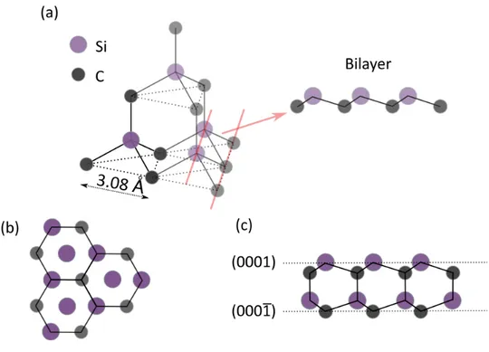
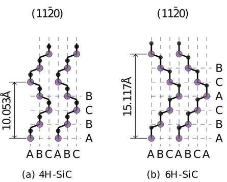
A single TMD layer is constituted by two layers of chalcogen atoms sandwiching another layer of a transition metal. They have the chemical formula MX2, where M is a transition metal (W, Mo, V, etc) and X is a chalcogen (S, Se and Te). The two most common structural phases are the hexagonal (2H) and octahedral (1T), which differ in the stacking: ABA and ABC respectively (Fig. 1.4) Fig. 1.4 Lattice structure of TMDs in the three most stable phases. Top view in the top panels and side view in the bottom panels. Adapted from 58 In the 2H phase, the two chalcogen atoms in different atomic planes occupy the same position on top of each other. The 1T phase instead can be regarded as a structural transition from the 2H phase where the X atoms on one side of the M atoms are shifted to coincide (in the top view) with the centers of the hexagons formed by M atoms and other X atoms59. Depending on the atomic species, one of the two structure is stable and the other either absent or metastable58. In addition to 2H and 1T also the 1T’
(distorted octahedral) can occur. It is similar to 1T, however it shows a distortion in the W coordination which alters its electronic properties60. The most studied classes of TMDs are the ones having Mo and W as transition metals. In WS2 and MoS2 the most stable is the 2H phase53, whereas WTe2 is stable in 1T in bulk form at room temperature and 1T’ in monolayer form. Fig. 1.5 Side view of WS2 unit cell. The atomic distances are reported The WS2 unit cell is formed by two atoms of S and one of W displaced as shown in Fig. 1.5. Qualitatively, it has the same lattice vectors of graphene, hence the same BZ. However, their sizes differ as WS2 lattice parameter is 𝑎 = 3.16 Å61. The base atoms of S and of W are placed in position d µ] dµk and d¶ , respectively d µ]= z0,√{j ,°·k| dµk= z0,√{j ,°·k| d¶ = (0,0,0) (2) where ℎ = 3.12 Å is the height of the layer.
ELECTRONIC PROPERTIES
Due to the wide plethora of chemical species, TMDs show a broad range of electronic properties from (semi)metallic to insulating. In the text below,the electronic properties of WS2 will be discussed, which qualitatively speaking are similar to those of MoS2, MoS2 and WSe2. 53. Bulk WS2 is an indirect semiconductor with a band gap of ~1.3 eV62, with the maximum of the VB in 𝚪 and the minimum of the conduction band (CB) in K. In 𝚪, the d-orbitals of W hybridize with the pz-orbitals of the chalcogen atoms. This out-of-plane displacement is strongly affected by the number of layers. It lowers in energy going towards the monolayer form. The states in K are purely in-plane, therefore they remain unaffected when lowering the dimension of the system61. At the monolayer limit the system displays a direct band gap whose magnitude is ~2 eV (see Fig. 1.6)62. Fig. 1.6 Evolution of the band structure of WS2 with the number of layers, the band gap turns from indirect to direct passing from bulk to monolayer. Adapted from62. This transition has been explored in terms of PL, i.e. the emission of light consequent to the recombination of an electron in the CB with a hole in the
VB. Indeed, PL increases mowing towards the single layer as displayed in Fig. 1.763. Fig. 1.7 PL spectra collected from WS2 monolayer (black) and bilayer crystals (red). The shift in the PL emission energy is due to the shrinking of the band gap in the bilayer crystal. Adapted from 63. In 2d materials with hexagonal lattice structure, the 𝐊 and 𝐊′ valleys are connected by time reversal symmetry. To access one valley or the other it is necessary to have a measurable physical quantity that has odd parity under time reversal. The valley degree of freedom behaves as the spin. Up and down states have the same time reversal relationship of the valleys in 2d materials and they are distinguished by opposite values of magnetic moment. Therefore, the magnetic field can be used to select one of the two states.
As said before WS2 has a direct band gap in 𝐊 and 𝐊′ when monolayer. This suggests that polarized light can be used to access one valley or the other (Fig. 1.8) since selection rules at the base of optical transition have the right
exciton has already been demonstrated65 where PL is found to be strongly polarized with the same circular polarization as the incident light. Intervalley scattering is suppressed by the large momentum separation, leading to robust valley polarization.
Fig. 1.8 Optical selection rules in 𝐊 and 𝐊′. Light with different polarization promotes
carriers in different valleys. Adapted from 55.
It is important to mention that WS2 manifests a big spin-orbit coupling. This implies that at the K point the bands display a splitting that lifts the degeneracy of the spin. Considering the inversion symmetry breaking and the selection rules mentioned before, the spin degree of freedom is locked to the valley, meaning that the excited carriers resulting from optical pumping will also be spin-polarized55.
SYNTHESIS OF WS2
When bulk, WS2 is a layered material as graphene and as graphene it can be exfoliated applying the same method of scotch tape exfoliation. However, as explained previously, this approach lacks of scalability. Other techniques have been used to synthesize monolayer WS266,67. Among them, CVD65,68,69 and metalorganic-CVD (MOCVD)70–72 are definitely the most
adopted to obtain highly crystalline and large area monolayer WS2. CVD is the technique adopted in this work to grow WS2 and it will be extensively described in chapter 3. It relies on the reduction and subsequent sulfurization of tungsten trioxide (WO3) powder24. The S, at first solid, is evaporated in a controllable way in order to be delivered next to the W source. After the reaction, the WS2 molecules diffuse on the target substrate where they form the 2d crystal. The process is cost-effective and of simple implementation. MOCVD relies on the delivery of reactants in gas from, starting from vapor phase metal-organic complex molecules. They contain the desired atom, surrounded by a volatile compound that facilitates the material delivery. Once in contact with the hot substrate, they denaturize into more light byproducts, which are pumped away, leaving the metal behind. The metal atoms then react with chalcogen atoms deposited in the same fashion67. Typically used compounds are M(CO)6 - where M is a metal such as W – and (C2H5)S – where S is a chalcogen such as sulfur. This technique can lead to fully covered substrates such as SiO2/Si++. However, dealing with metal-organic compounds is not trivial and the chemistry behind the reaction can be more complicated than expected.
Other effective techniques for the production of TMDs are LPE and sulfurization of tungsten oxide layers deposited by atomic layer deposition (ALD). The former is very similar to the technique used for graphene as it uses sonication in common solvents such as NMP or isopropanol (IPA) with subsequent centrifugation and decantation. This approach is ideal to have large scale production of 2d materials for low-tech applications such as reinforcement of composite materials66. ALD offers the possibility of depositing a layer of a selected oxide on a substrate by exposing its surface
species are delivered sequentially. Song and coworkers demonstrated the successful growth of WS2 using this approach73.
Fig. 1.9 ALD of WS2, starting from WO3 subsequently sulfurized. Adapted from 73
Fig. 1.9 reports the synthesis scheme. First a layer of W is deposited starting from the chemical precursor WH2(iPrCp)2 that decomposes leaving metallic atoms on the substrate. Subsequently, using oxygen plasma it is possible to oxidize the structure leading to a layer of WO3. The material now is sulfurized at high temperature by means of a gas mixture of argon (Ar) and H2S. This technique allows for high thickness uniformity over the entire substrate but presents drawbacks such us the use of dangerous precursors and the formation of many grain boundaries (e.g., grain size of tens of nanometers). However, carrier mobilities of about 4 cm2/Vs have been recently reported73, indicating a rapid development in the growth control. By offering significant prospects in terms of scalability, in the future this technique shall be optimized to produce wafer scale 2d semiconductors.
Another technique which has been adopted, although in a limited way, to obtain TMDs, is molecular beam epitaxy (MBE). MBE is performed in ultra-high vacuum (UHV) (10-10 bar), with the reactants introduced in the form of molecular beams by vaporizing a source solid material. The UHV
environments allows for the ballistic transport of the chemical species on the substrate. Nevertheless, TMDs produced via MBE typically present poor crystal quality and low coverage74,75.
HEXAGONAL BORON NITRIDE, PROPERTIES AND
SYNTHESIS
h-BN is constituted by nitrogen (N) and boron (B) atoms arranged in a hexagonal lattice. Its lattice parameter is 𝑎 = 2.51 Å, slightly larger than that of graphene. When bulk, h-BN is a layered material kept together by vdW forces. Fig. 1.10 h-BN lattice structure, with the d1 and d2 base atoms of B in yellow and N in cyan. a1 a2 are the base vectors. (b) Representation of h-BN lattice in reciprocal space, with Γ−Μ−Κ−Γ the irreducible area of the BZ. The absence of dangling bonds makes this structure extremely flat. Also in this case the sp2 hybridization is responsible for the planar structure of the 𝜎 bond, However, with respect to graphene, h-BN is formed by two inequivalent sublattices formed by the two different chemical species. This
the h-BN crystal structure and its relative reciprocal lattice, with the irreducible area of the BZ highlighted by the special points G-M-K-G.
ELECTRONIC PROPERTIES
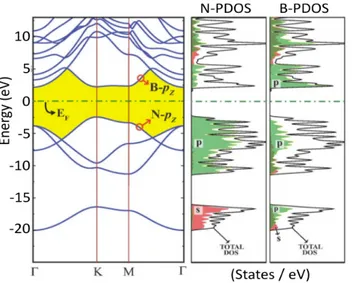
h-BN is a wide gap semiconductor77,78. It does not show any light absorption in the visible range, however in the ultraviolet region it displays good adsorption and photoluminescence79. In Fig. 1.11 h-BN band structure is displayed including the projected density of states (PDOS) over B and N states. Conduction and valence bands are due to B and N states, respectively.
PREPARATION OF H-BN
Nowadays, a lot of effort is being put on implementing techniques such as LPE80 and CVD81 to produce single layer h-BN. LPE, as in the case of graphene, has the advantage of scalability (at the expenses of crystallinity) which makes it the technique of choice for low-tech applications (e.g.,
Fig. 1.11 h-BN band structure and projected density of states on N and B orbitals. Adapted from (78)
insulating coatings/inks). Instead, CVD attempts on catalytic substrates typically yield polycrystalline multilayer h-BN82,83. Vacuum synthesis on catalytic substrates has yielded h-BN monolayers84, although in this case, transfer from the substrate and scalability remain significant issues. Hence, to date, the most popular technique to produce high-quality monolayer h-BN remains mechanical exfoliation21 (performed as reported in paragraph 1.2.3). When h-BN crystals tens of nanometers thick are requested, mechanical exfoliation is carried on by placing large bulk crystals on top of a commercially available scotch tape (blue tape semiconductor grade). Subsequently, the blue tape is back-folded in order to place the h-BN between two adhesive limbs, which are then pealed apart leaving on each side h-BN flakes of various thickness85. Fig. 1.12 Scheme of exfoliation process and deposition on a substrate. From left to right: Exfoliation of the crystal using two limbs of scotch tape. Deposition of one limb of scotch tape on a substrate. Pealing off of the scotch tape leaving the crystals on the surface. The latter can be further reduced by repeating the process many times on a new patch of scotch tape. The h-BN flakes are transferred on the desired substrate by pressing it against the adhesive tape (Fig. 1.12). Solvent cleaning is finally adopted to remove glue residues. With this method, a fine control over the number of layers is not possible. The high-pressure method presented by Watanabe and Taniguchi86 allows for obtaining bulk
Hopefully, in the next years, significant step forwards in synthetic techniques will yield high quality monolayer material thus speeding-up the development of all-2d-based technologies.
2D VERTICAL HETEROSTRUCTURES
Fig. 1.13 reports a comparison between a standard covalent heterostructure – the center of semiconductors research for more than 40 year87,88 – and a vdW heterostructure. In covalent heterostructures chemical bonds exist between different materials. Classical methods to produce covalent heterostructures are molecular CVD or MBE. If the thin film which is deposited has the same chemical composition of the bulk underneath, this method is known as homo-epitaxy; hetero-epitaxy otherwise12. In hetero-epitaxy, to ensure that the thin top-layer has high crystalline quality, its lattice structure should be as close as possible to that of the substrate. The epitaxial registry is very important to control the defects at the interface. Namely, combining materials with different lattice parameters creates defects, dislocation and even lattice breaking at the interface and this can be harmful for the performance of the device. In standard AlGaAs heterostructures, solutions like modulation doping are used in order to tune the electronic properties of the material without introducing defects. In such a way it is possible to obtain a 2d electron gas (2DEG) that can reach mobilities of µ~35x106 cm2/Vs13. The current silicon technology is based on the capability to create a sharp interface between doped Si and SiO2 keeping low the fabrication costs. Nevertheless, having chemical bonds limits the selections of materials available. vdW heterostructures – formed by staking 2d layered materials such as graphene, TMDs and h-BN – hold promises to overcome the abovementioned hurdles. Indeed, the lack of covalent bonds between the layers (see Fig. 1.13(b)) relaxes the constraints on the matching of the
lattice parameters. Hence, one can – in principle – combine any kind of layered material to form the desired heterostructure. In vdWH the properties of each constituting layer might be either significantly changed or remain seemingly unaltered. For instance, when placing TMDs on graphene, a gap is opened at the Dirac point in graphene as a consequence of the spin-orbit proximity effect23.
Fig. 1.13 Representation of a covalent heterostructure (a) and of a vdW heterostructures (b). In the first there are no chemical bonds between layers. Adapted from 89
In other cases, due to the weak interaction between the constituting layers, the electronic structure of each material is not altered. Therefore, within the full system, the properties of each single layer are preserved. For instance, when stacking graphene on h-BN, the electronic properties of the former are greatly enhanced as first demonstrated by Dean et al21. Recently, Banszerus and co-workers1 have demonstrated a record mobility for graphene (i.e., µ=3,000,000 cm2/(Vs)) by encapsulating it between two h-BN layers. On the contrary, on SiO2, the typical substrate adopted to realize graphene backgated devices, graphene transport properties are
inferior (e.g., typically a few thousands of cm2/(Vs))90. In fact, SiO2 displays a significant surface roughness that increases electron scattering in graphene. The extreme flatness and the absence of dangling bonds in h-BN, make it the perfect candidate to suppress undesired scattering. In the following chapters the electronic properties of the vdWH WS2 on graphene will be investigated and discussed in depth. SYNTHESIS OF 2D VERTICAL HETEROSTACKS Fabrication of 2d vertical heterostructures can be carried on with different approaches. As for every 2d material, the first to be demonstrated was mechanical exfoliation. Fig. 1.14 Diagram of the steps involved in the preparation of the viscoelastic stamp and the deterministic transfer of an atomically thin flake onto a user-defined location (for instance another atomically thin flake). Adapted from 91 Nowadays, by using Polydimethylsiloxane (PMDS) stamps, it is possible to transfer exfoliated 2d materials one on top of each other in a very clean and controlled way91,92. The stamp is a thin layer of commercially available viscoelastic material which is adhered to a glass slide to facilitate its
handling. The crystals to be transferred are deposited onto the viscoelastic layer by mechanical exfoliation. The surface of the stamp is inspected under the optical microscope to select the thinner flakes due to their faint contrast under normal illumination. The stamp is then attached to a three-axis manipulator with the flakes facing towards the sample. As the stamp is transparent, one can see the sample through it and thus it is possible to align the desired flake on the target surface at sub-micrometer resolution91. In Fig. 1.14 the various steps of the transfer method are depicted.
The advantage of this technique is its versatility as it can be applied to transfer any layered material (even obtained in different ways). However, this method is extremely cumbersome and does not offer any scalability, since the heterostructures are literally hand-made one by one. CVD synthesis offers nice advantages for the production of vdW heterostacks. By being a bottom-up approach, CVD synthesis offers a fully scalable way to produce heterostacks. Furthermore, this approach allows for a van der Waals epitaxy (vdWE), i.e., the synthesis of azimuthally aligned heterostructures. As a 2d layer is grown on top of another, it is influenced by the crystal structure of the substrate which might therefore induce on it a well-defined register. The concept of vdWE has been introduced almost 20 years ago93 by A. Koma, Before this work a few groups demonstrated vdWe of 2d heterostacks65,85,94,95. For instance, Li and coworkers96 demonstrated the epitaxial growth of GaSe on graphene via CVD. Structural analysis (Fig. 1.15) revealed that approximately 50% of the GaSe domains were oriented with a ~10° interlayer rotation with respect to the underlying graphene (the most energetically stable azimuthal orientation as also confirmed by theoretical calculations). Nevertheless, the fine control over the heterostack formation process remains a huge challenge.
At the time when this work started, no work had reported the synthesis of WS2 on graphene. In fact, although graphene growth had matured to a level where the synthesized films and the mechanically exfoliated ones had comparable quality, WS2 synthesis had still to be perfected and implemented on 2d substrates. Fig. 1.15 SAED pattern of GaSe on graphene obtained via TEM analysis. The two crystals are misaligned by 10.7°. Adapted from (47) The synthesis of WS2 over graphene and h-BN is thoroughly discussed in Chapter 4. APPLICATIONS OF VAN DER WAALS HETEROSTRUCTURES
To date, a large number of potential applications for vdW heterostacks have been proposed, spanning from flexible electronics to DNA detection97. In the following, vertical tunnel field effect transistor (TFET) for low power and fast electronics and light detection will be discussed. Despite not having specifically treated TFETs in this thesis, their working principle
relies on the epitaxial alignment extensively studied for 2d vertical heterostructures in the following chapters. Conversely, the topic light detection is discussed as vdW-based photodetectors are reported in chapter 6. Indeed, for both these applications the crystalline quality and the epitaxial alignment of the grown heterostacks are extremely relevant. To date, most devices for (opto)electronics have been demonstrated using mechanically exfoliated flakes. In exfoliated vertical stacks no control on the epitaxial alignment can be operated, while CVD synthesis offers – as discussed- the possibility to implement vdWE.
TUNNELING DEVICES FOR LOW-POWER ELECTRONICS APPLICATIONS
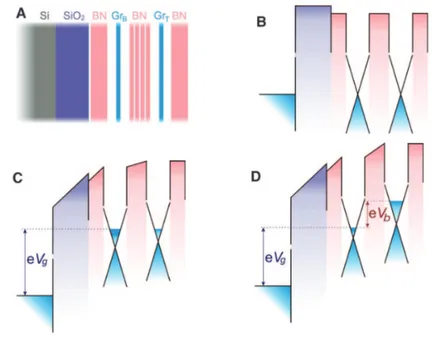
The possibility to combine two-dimensional semiconductor, conductor and insulating materials in a vertical stack regardless of their lattice parameter opens to route to a new class of electronic devices. Vertical tunneling transistors are devices that modulate the tunnel barrier between metals and semiconductors rather than the thermoionic emission barrier. This allows this class of devices to be faster and to consume less power with respect to traditional bulk materials-base- transistor98. In a classical vertical tunneling transistor graphene is piled with h-BN which acts as a tunnel barrier (Fig. 1.16)99. h-BN is ideal for this purpose, having a wide band gap and a flat surface. Also, other materials with a non-negligible band gap can be interfaced with graphene and used as tunnel-barrier, such as for example the TMD studied in this work, WS2100. Azimuthal alignment between the two conductive layers separated by the barrier plays a major role, since for tunneling to occur the momentum conservation has to be fulfilled, therefore the BZs of the layers have to be aligned. When the lattices of the two materials forming the vertical heterostack are strongly
involve phonons or impurities at the interface. Hence, in order to realize efficient vertical tunneling transistors made of graphene and a TMD, it is crucial to understand and control the band structure alignment within the heterostructure. This work explores this aspect in chapter 4.
Fig. 1.16 Graphene field-effect tunneling transistor. (A) Schematic structure the experimental devices. (B) The corresponding band structure with no gate voltage applied. (C) The same band structure for a finite gate voltage Vg and zero bias Vb. (D) Both Vg and Vb are finite. Adapted from 99
VAN DER WAALS HETEROSTRUCTURES FOR LIGHT DETECTION
Another class of devices that can be realized with vdWH are those dedicated to light detection. 2d materials that possess a direct band gap, such as monolayer TMDs, can be used to fabricate photodetectors active in the infrared and visible range. By combining TMDs’ optical absorbance
with the outstanding transport properties of graphene efficient photodetectors have been demonstrated22. The simplest device structure is that obtained by vertically stacking graphene, as the channel material, and a TMD, as the optically active layer. This is an efficient architecture for phototransistors (Fig. 1.17). The charge transfer from the optically active layer to the channel ensures a fast detection of the incident light101. A part of this work is focused on the fabrication of photodetectors based on the interface graphene/WS2 (see Chapter 6). Fig. 1.17 Scheme of a hybrid WS2/Gr based device, WS2 is the active material, whereas graphene acts as fast channel.
EXPERIMENTAL TECHNIQUES
This chapter introduces the experimental technique used in this work. Particular focus is put in the discussion of surface science techniques such as angle resolved photoemission spectroscopy (section 2.2), low energy electron diffraction (section 2.4) and microscopy (section 2.5) since they led to one of the major results reported in this work, mostly obtained at the ELETTRA synchrotron facility in Italy. Other routinely used techniques such as Raman spectroscopy are also addressed. In particular, one entire section (2.8) is devoted to Raman applied to graphene and other 2d materials as this discussion is instrumental for a better understanding of the data presented in this thesis.
PHOTOELECTRON SPECTROSCOPY
Photoelectron spectroscopy (PES) is a technique used to study the electronic state and the chemical composition of the surface region of a sample (solids, liquids or gases). Its working principle is based on the photoelectric effect discovered by Hertz in 1887 and explained by Einstein in 1915. The photoelectric effect is a phenomenon involving the expulsion of electrons from a material when it absorbs light with sufficient energy. Specifically, the term PES refers to a number of techniques depending on the source of the exciting radiation. The excitation source is a high-energy radiation spanning from ultraviolet light (for instance generated by a helium (He) lamp) to X-ray (for instance coming from a synchrotron source). The electromagnetic radiation is directed towards the target material. Once the radiation impinges on the material, emitted (photo)electrons are generated. Such electrons are then adsorbed by an analyzer whose work function sets the reference for the measurement of the kinetic energy. The energy conservation law allows calculating the
binding energy of the electron starting from its kinetic energy and, therefore, information about the energy levels of the material can be extracted.
𝐸»‰¼= ℎ𝜐 − 𝜙¿− 𝐸À = ℎ𝜐 − 𝐸Áj (1)
Where ℎ𝜐 is the energy of the incident photon, 𝐸À is the binding energy
calculated with respect to the Fermi Level and 𝜙¿ is the work function of the analyzer referred to the Fermi energy of the system (the same of the sample as long as they are put in electrical contact). 𝐸Áj is the energy of the vacuum level. In the energy distribution of the relevant spectra, shown in Fig. 2.1, N(E) is the DOS in the sample (lower left) and for the revealed photo emitted electrons (upper right). Fig. 2.1 Scheme of the energies involved in a photoelectron emission process from a solid. N(E) is the energy distribution of the photoemitted electrons. Adapted from 102
The non-dispersive states represent the core levels of the system. The collected electrons are shifted up in energy by the photon energy minus the work function necessary to inject the electrons in the analyzer from vacuum. This scheme is very simple and does not take into account the presence of inelastic scattering events, which would give rise to additional features at different binding energies.
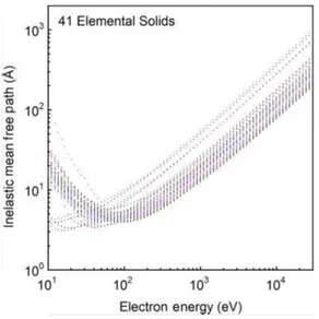
Fig. 2.2 Inelastic mean free path in function of impinging electron energy calculated for 41 materials. From 103
The electrons that experience multiple inelastic scattering events are called secondary and are present mainly in the lower part of the kinetic energy spectrum. The inelastic scattering puts a limit to the distance that electrons can travel before escaping the substrate. It strongly depends on the kind of material and on the energy of the impinging electron. The average distance travelled by an electron before losing energy is called inelastic mean free path (IMFP). The IMFP for different elemental materials and in function of the impinging electron energy is displayed in Fig. 2.2 as calculated in Ref.103.
In photoemission, the escape depth of the electrons is between 5 and 10 Å in the energy range 20–1000 eV. Therefore, for photoemission experiments, the sample surface should be atomically clean. UHV environment is typically required in order to avoid any unwanted scattering event with gaseous species in the chamber.
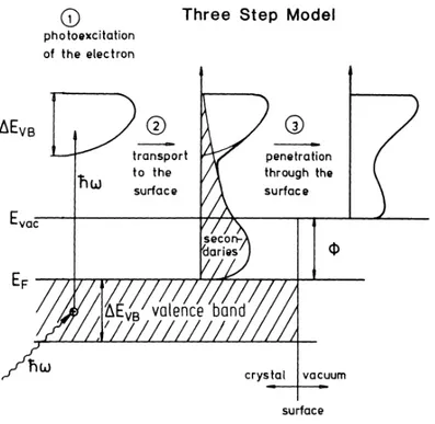
Fig. 2.3 Three step model describing the photoelectrons dynamics before escaping the material. 1) Photoexcitation of electron 2) transport to the surface 3) penetration through the surface. From 102
The photoemission process can be phenomenologically described with the three-step model first proposed by Berglund and Spicer104. This model identifies three independent events within the full photoemission phenomenon. The three steps (sketched in Fig. 2.3) are:
(2) Migration of the electron towards the surface
(3) Penetration of the electron into the barrier at the interface material-vacuum and escape into the vacuum
However, in order to simplify the description, the so called one-step model is here adopted, where the initial and final states only are taken into account102.
When the electromagnetic field, described by the potential vector A impinges on the substrates it promotes one electron in its excited state. This process is described by the well-known Fermi Golden Rule 105: 𝑤 ‰Ä ∝ 2𝜋 ℏ Ç< 𝜓Ä Çℋ‰¼É|𝜓‰ >|k𝛿(𝐸Ä− 𝐸‰− ℎ𝜐) (2)
Where ℋ‰¼É is the interaction Hamiltonian, 𝜓Ä and 𝜓‰ are the final and
initial state respectively. The approximated form for ℋ‰¼É, neglecting second order processes, is ℋ ‰¼É = 𝑒 𝑚𝑐𝐴 ∙ p (3) where p is the momentum operator.
The matrix element depends on the photon energy, but also on the experimental geometry. The matrix element is a fundamental quantity when considering polarized light and it could give a complete suppression of photocurrent. The polarization of the incident light is defined by the orientation of the electromagnetic field with respect to the mirror plane, i.e.
the plane orthogonal to the substrate where lies the wave vector. If the electromagnetic field is orthogonal to the mirror plane the beam is defined as s-polarized, if it lies on the mirror plane it is defined as p-polarized106.
ANGLE-RESOLVED PHOTOELECTRON SPECTROSCOPY
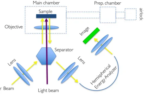
ARPES is a PES technique that records the number of photoemitted electrons at a given kinetic energy and emission angle with respect to the sample. This technique takes advantage of ultraviolet or X-ray radiation to extract electrons from the investigated sample. Fig. 2.4 ARPES set up scheme. Electromagnetic radiation provide enough energy to the sample to leave the first layers of the substrate and travel towards the analyzer.
As mentioned above, the radiation can be generated by a number of sources such as helium He lamp or synchrotron radiation. Thanks to the energy and momentum conservation laws it is possible to extract the kinetic energy and the momentum of the electrons before they are emitted from the crystal. In this way it is possible to obtain momentum-energy
typical experimental set-up for ARPES measurement is sketched in Fig. 2.4. The radiation is shone over the sample. The photoemitted electrons are directed by means of magnetic lenses into a hemispherical analyzer. Here, the electrons are separated in trajectory according to their energy by means of an electrostatic field. Finally, the electrons are collected by a detector. The detectors are made by a fluorescent screen which emits light when hit. A CCD camera reconstructs the energy dispersion of the crystal subsequently collecting the outgoing light. With modern detectors it is possible to obtain 2d maps of the energy dispersion and also reconstruct the Fermi surface topology.
Photoemitted electrons can also be collected to obtain an image of the surface (photo-emitted electrons are originated from a very shallow layer). Variation in electron emission is used to generate image contrast. This technique is called photoemission electron microscopy (PEEM) or XPEEM when X-rays are used as excitation source.
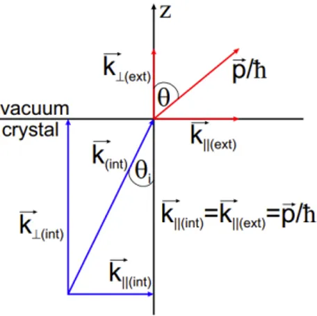
During the electron extraction process, the parallel component 𝑘|| is
conserved, thanks to translation symmetry in the x-y plane across the surface. Making the assumption that the momentum carried by the photon 𝑝η= ℎ𝜐/𝑐 is negligible compared to the crystal momentum of the electron ℏ𝑘 ≫ 𝑝η, ensures a vertical transition in the reduced zone scheme, thus 𝐤Ä = 𝐤‰. Hence, the von Laue equation 𝐤Ä = 𝐤‰+ 𝐆 is fulfilled, where 𝐆 is a base vector of the BZ. Indeed, experiments are usually performed using photon energy lower than 100 eV, which correspond to a momentum of Î
ℏ≃ 0.05 Å
°]. Another assumption made to simplify the
description of the system is the so-called sudden approximation, namely the electron is supposed to be extracted instantaneously from the material with no time to interact with the remaining N-1 electrons. This allows us to