UNIVERSITY
OF TRENTO
DIPARTIMENTO DI INGEGNERIA E SCIENZA DELL’INFORMAZIONE
38123 Povo – Trento (Italy), Via Sommarive 14
http://www.disi.unitn.it
A NOVEL DESIGN METHODOLOGY FOR INTEGRATION OF
OPTIMIZED WIDEBAND ELEMENTS WITH APERIODIC ARRAY
TOPOLOGIES
L. Lizzi, G. Oliveri, M. D. Gregory, D. H. Werner, and A. Massa
January 2011
A Novel Design Methodology for Integration of Optimized Ultra‐
Wideband Elements with Aperiodic Array Topologies
(1)L. Lizzi, (1)G. Oliveri, (2)M. D. Gregory*, (2)D. H. Werner, and (1)A. Massa
(1) ELEDIA Group ‐ Department of Information Engineering and Computer Science
University of Trento, Via Sommarive 14, I‐38050 Trento, Italy
[email protected], [email protected], [email protected] (2) Department of Electrical Engineering The Pennsylvania State University, University Park, PA 16802, USA [email protected], [email protected] Introduction
The recent development of many new ultra‐wideband (UWB) array technologies has created a demand for antenna elements that can effectively operate over similar bandwidths. For example, the polyfractal [1] and RPS [2] topologies are capable of exhibiting remarkably wide frequency bandwidths on the order of 20:1, 40:1 or even more, depending on the array size. Often, the antenna elements that are capable of these extended bandwidths begin to develop several lobes in the radiation pattern and generate increased cross‐polarized radiation at their upper range of operating frequencies. A new type of ultra‐wideband antenna has been developed based on a spline‐shaping technique and a particle swarm algorithm (PSO) [3]. With proper attention to the radiation pattern, cross‐polarization, and return loss in the PSO cost function, this method is capable of producing UWB antenna elements that minimize all the aforementioned undesirable characteristics, making them very suitable for use in UWB array systems with bandwidths up to 4:1 and perhaps even wider.
Antenna Synthesis
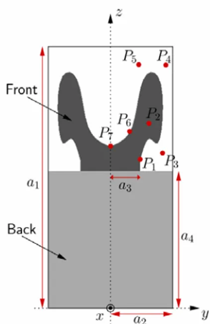
The proposed UWB antenna element is based on optimized copper layers on a dielectric substrate. Figure 1 shows the layout of the top and bottom copper layers, with the spline points and dimensions highlighted. The particle swarm algorithm is tasked with finding the best set of parameters that minimize the cost function in (1). The function contains contributions from the input S‐parameters and the cross‐polarized radiation,
given in (2). The constants and represent the S‐parameter and cross‐polarized
gain goals, here set to ‐10 dB and ‐30 dB, respectively. Equation (2) computes the spatially averaged cross‐polarized gain at Q = 5 points distributed over the radiation pattern. The cost function is evaluated over a frequency range of 6 GHz ≤ f ≤ 18 GHz for a 100% fractional bandwidth. The 50 Ω antenna feed which bridges the top and bottom copper structures is located at y = 0 and z = a4. The substrate is fixed at 0.8 mm thick and has electrical properties of εr = 3.38 and δt = 0.0025. T s11 gˆφT
( )
( )
∫
⎪⎭⎪⎬⎫ ⎪⎩ ⎪ ⎨ ⎧ − + ⎪⎭ ⎪ ⎬ ⎫ ⎪⎩ ⎪ ⎨ ⎧ − = 2 1 ˆ ˆ ˆ , 0 max , 0 max 11 11 11 f f T T T T COST df g g f g s s f s F φ φ φ(1)
( )
∑
(
)
= ⎟ ⎠ ⎞ ⎜ ⎝ ⎛ = = − = Q q q f q g Q f g 1 , 3 3 , 2 1 ˆφ φ θ π φ π(2) Antenna evaluation is carried out with FEKO [4], using a truncated dielectric as shown in Figure 1. The particle swarm algorithm was configured for a population size of 6 particles and required approximately 200 iterations to reach an acceptable solution, using 7 hours of CPU time on an Intel® Core2 processor. The resulting optimized parameters are (in mm): p1=(2.50,12.33), p2=(3.25,15.11), p3=(4.26,12.44),
p4=(4.73,20.03), p5=(2.46,17.82), p6=(2.16,14.39), p7=(0.00,13.56), a1=21.93, a2=5.25,
a3=2.50, and a4=11.38. Figure 2a shows the input performance of the optimized
antenna, exhibiting a very large 112% fractional bandwidth (5.5 ‐ 19.5 GHz) with |s11| ≤ ‐
10 dB. Figure 2b shows the far‐field cross‐polarized (gφ) and co‐polarized (gθ)
components in the xy‐plane (θ = π/2) at two select frequencies. The cross‐polarized component is very low compared to the co‐polarized gain, exhibiting values lower than ‐ 24 dBi and ‐19 dBi at 9 GHz and 15 GHz, respectively. Moreover, the antenna has good omnidirectionality, as indicated by the nearly flat co‐polarized gain component over the entire φ‐range. Ultra‐Wideband Array Layout
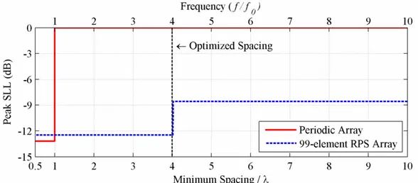
Next, a suitable ultra‐wideband array layout is generated using the RPS technique introduced in [2]. A two‐stage design using nine subarrays of 11 elements each was selected for an array of 99 elements total. The layout was optimized at a minimum element spacing of dmin = 4.0 λ, resulting in a maximum peak sidelobe level of ‐12.5 dB.
The array is configured for dmin = 1.0 λ at the lowest operating frequency (f0) of 6 GHz,
with element locations as shown in Figure 3. At this lowest operating frequency, the average and maximum element spacings are 1.3 λ and 3.04 λ, respectively. Figure 4 shows the performance of the array over an extended bandwidth, demonstrating a usable peak sidelobe level of about ‐8.6 dB even up to 10 f0.
Complete Ultra‐Wideband Array Performance
Lastly, computed radiation patterns at 9 GHz (dmin = 1.5 λ) and 15 GHz (dmin = 2.5 λ) were
created by combining the element patterns in Figure 3 with the array factor of the layout in Figure 4. The patterns exhibit very low sidelobe levels, even at a large minimum element spacing of 2.5 λ. Because of these large element spacings, mutual coupling can be expected to be very small and have little effect on the impedances of the elements, yielding actual performances very close to that of the pattern multiplication predictions.
Conclusions
The spline‐based antenna synthesis technique has been shown to be an effective solution to the element performance requirements of the new UWB array technologies. An antenna with strong linear polarization and good omnidirectionality over a large 112% fractional bandwidth was optimized and placed in a suitable array layout, yielding a novel design for a practical UWB array. The optimized aperiodic element locations created by the RPS method allow full use of the antenna bandwidth without the plague of high peak sidelobe levels or grating lobes typically seen with large element spacings.
References
[1] J. S. Petko and D. H. Werner, “The Pareto Optimization of Ultrawideband Polyfractal Arrays,” IEEE Trans. Antennas. Propagat., Vol. 56, No. 1, pp. 97‐107, 2008.
[2] M. D. Gregory and D. H. Werner, “Optimized Ultra‐wideband Linear Raised‐power‐ series Antenna Arrays,” IEEE International Symp. on Antennas and Propagat., Charleston, SC, June 1‐5, 2009.
[3] L. Lizzi, F. Viani, R. Azaro, and A. Massa, “A PSO‐driven spline‐based shaping approach for ultrawideband (UWB) antenna synthesis,” IEEE Trans. Antennas.
Propagat., Vol. 56, No. 8, pp. 2613‐2621, 2008.
[4] FEKO. EM Software and Systems – S.A. [Online]. Version 5.4. Available at: www.emssusa.com.
Figure 1: Antenna geometry.
(a) (b)
Figure 2: Magnitude of s11 over frequency (a) and co‐polarized and cross‐polarized gain
Figure 3: Element locations (in wavelengths) at 1 λ minimum element spacing, corresponding to the lowest operating frequency (6 GHz, λ = 5 cm).
Figure 4: Bandwidth performance of the optimized RPS array and a standard periodic array. All elements are uniformly excited and the arrays are steered to broadside.
Figure 5: Normalized power patterns at 9 GHz (a) and 15 GHz (b) for the ultra‐wideband array
when steered to broadside. The array factor (red) shows only the effect of the ultra‐wideband array, while the total pattern (blue) combines the array factor and element pattern (at each respective frequency). The peak sidelobe level at both operating frequencies is ‐12.5 dB.