A Study of
Additive
Manufacturing
Applied to the
Design and
Production of
LED Luminaires
Scuola del Design
MSc. in Design & Engineering Anno Accademico 2013 / 2014
Academic Supervisor:
Marinella Levi
Industrial advisor:
Valentina Folli
Graduating student:
Pedro Sanín Pérez
Matricola 797808
1. Background ...
1.1. Introduction ...
1.2. Project Background ...
1.3. Justification ... 1.3.1. Why Additive Manufacturing? ... 1.3.2. Why LED? ... 1.3.3. Why apply AM to the production of new LED luminaires? ...
1.4. Personal Motivation ... 2. Objectives ... 2.1. General Objective ... 2.2. Specific Objectives ... 2.3. Project scope ... 3. Methodology ...
3.1. The Innovation Process ...
3.2. The New Concept Development Model ...
3.3. Creative Problem Solving ...
3.4. The Mixed Model Methodology ...
4. Literature Review ... 4.1. Additive Manufacturing ... 4.1.1. Application Field ... 4.1.2. AM Process Review ... 4.1.3. Materials ... 4.1.4. Design for AM ... 4.1.5. Future Research ... 4.2. LED Lighting ... 4.2.1. Basics principles of Lighting ... 4.2.2. LED Basics ... 4.2.3. LED Luminaires ...
4.3. AM applied to LED Lighting ... 4.3.1. Case Study 1: Printed Optics ... 4.3.2. Case Study 2: Advances in heat sink performance with DMLS . 4.3.3. Case Study 3: Heat Transfer Enhancement ...
5. Analysis ...
5.1. Applicability of AM technologies and materials ... 5.1.1. Heat management ... 5.1.2. Optical qualities ... 5.1.3. Electrical Conductivity ...
5.2. Analysis of lighting applications (benchmarking) ...
5.2.1. Luminaires Created by Additive Manufacturing ... 5.2.2. Recent Commercial LED Luminaires ...
01 01 01 02 03 04 06 09 11 11 11 11 12 12 13 14 16 18 18 20 22 31 35 39 41 41 48 55 69 69 72 73 75 75 75 81 82 85 85 92
6.2. Functional and Morphological Analysis ... 6.2.1. Functional Analysis ... 6.2.2. Morphological Analysis ... 6.2.3. Product Architecture ... 7. Design ... 7.1. Design concepts ... 7.1.1. Conceptual references ... 7.1.2. Design concept 1: Arista ... 7.1.3. Design concept 2: Air on the G String ...
7.2. Concepts selection and development ...
7.2.1. Pendant, floor and wall variations ...
7.3. Detailed Design ...
7.3.1. Selection of internal components ... 7.3.2. Detail design of the body ...
8. Validation and Results ... 8.1. Design validation ... 8.1.1. Printing Process ... 8.1.2. Part assembly ... 8.1.3. Copper plating ... 8.1.4. Light generation ... 8.1.5. Heat dissipation ... 8.2. Design improvements ... 8.2.1. Arista V2 ...
8.2.2. Printing and copper plating of Arista V2 ... 8.2.3. Arista Pendant ...
8.3. Cost validation ... 9. Conclusions and Analysis ...
9.1. Project Conclusions ... 9.2. Future research ... 10. References ... 10.1. Bibliography ... 10.2. Websites ... 11. Acknowledgements ... 105 105 107 111 114 115 116 120 123 126 127 130 130 132 137 137 137 142 143 145 147 149 149 152 154 155 157 157 159 161 161 165 167
Chapter 1
Figure 01: Why AM? Figure 02: Why LED?
Figure 03: Average lighting efficacy and cost per bulb projections Figure 04: Why AM applied to LED?
Chapter 3
Figure 05: The Innovation Process (Bruce Archer, 1971) Figure 06: The New Concept Development Model Figure 07: Creative Problem Solving
Figure 08: The Mixed Model Methodology
Chapter 4
Figure 09: Overview of additive processing technologies Figure 10: Procedure for fused deposition modeling Figure 11: Staircase effect on curved parts
Figure 12: Classification of AM processes based on different mechanisms of laser-material interaction
Figure 13: Schematic cycle of the SLS process Figure 14: Classification of metal AM processes Figure 15: Visible Spectrum of light
Figure 16: Luminous flux generated by a light source Figure 17: Iluminance
Figure 18: Luminous intensity Figure 19: Luminance
Figure 20: Photometric curve of a light source Figure 21: Light color range measured in °K Figure 22: Warm white, white and cool white Figure 23: structure of a LED package Figure 24: Three basic levels of LED Figure 25: LED panels, spot, strip and COB
Figure 26: Segmentation for cool and warm light binning Figure 27: Optics produced by LED Engin
Figure 28: Halos generated from narrow, medium, wide and elliptical optics Figure 29: LED Collimator
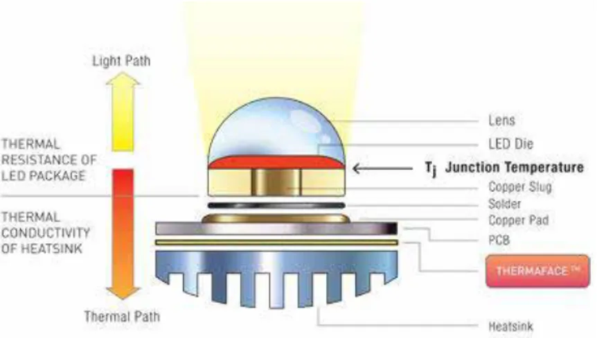
Figure 30: LED drivers by BAG electronics Figure 31: Types of light distribution in luminaires Figure 32: Light Fixture (Luminaire) Types Figure 33: Example of LED thermal path Figure 34: Examples of common heat sinks
Figure 36: Heat sinks manufactured by DMLS
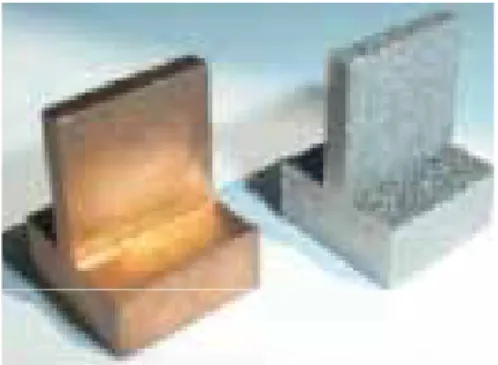
Figure 37: Picture of milled copper and DMLS Aluminum alloy heat sinks
Chapter 5
Figure 38: Unterlinden pendant lamp, Herzog & De Meuron for Artemide (2014)
Figure 39: Florensis, Ross Lovegrove for Artemide (2013)
Figure 40: Printed and welded part made with Weld3D technology Figure 41: Metallic printed part by MatterFab
Figure 42: Custom nylon and copper plated heat sink. Figure 43: Repliform’s electroplating process and results
Figure 44: Results of Luxcexcel’s Printoptical in comparison to other AM technologies
Figure 45: Tizio, Richard Sapper for Artemide.
Figure 46: Diagram of curved layer deposition used to create continuous circuits
Figure 47: Searching the term “lamp” in Thingiverse produced 1116 results (15/03/2015)
Figure 48: 3D printed lamps designed by Nervous System
Figure 49: Hyphae lamp by Nervous System, comercialized through Shapeways
Figure 50: Bloom lamp, MGX by Materialise Figure 51: Lilly lamp, MGX by Materialise
Figure 52: Aphillia and Rhizaria lamps by .exnovo Figure 53: Knot lamp by Ingo Maurer (2013) Figure 54: Chapo lamp, Phillipe Starck for FLOS Figure 55: Aplomb, Studio Lucidi & Pevere for Foscarini Figure 56: Clay printed parts by +Lab, Politecnico di Milano Figure 57: One Chair, Konstantin Grcic for Magis
Figure 58: IN-EI, Issey Miyake for Artemide Figure 59: Etch, Tom Dixon
Chapter 6
Figure 60: Symbols used to represent flows and functions throughout the system
Figure 61: Black Box analysis of a LED Luminaire Figure 62: Functional Structure of a LED Luminaire
Figure 63: Volumetric representations of the elements that constitute the luminaire
Figure 65: Four examples of artwork by digital artist Andy Gilmore Figure 66: Initial exploratory sketches
Figure 67: Arista ceiling fixture concept design Figure 68: Arista ceiling fixture concept design (2)
Figure 69: Arista ceiling fixture characteristics and components Figure 70: Air on the G String concept design
Figure 71: Air on the G String concept design (2)
Figure 72: Air on the G String components and characteristics Figure 73: Arista 2 pendant and floor variations
Figure 74: Arista 2 wall and floor variations
Figure 75: Arista 3 variation shown as pendant lamp Figure 76: CREE XLamp CXA 2530
Figure 77: Comparison of different COB lamps using CREE Inc.’s Product Characterization Tool
Figure 78: QLT Flat Box 700mA, 23W
Figure 79: LEDiL’s Angelina reflector designed specifically for CREE COBs Figure 80: Recommendations to improve the model done by +Lab Milano Figure 81: Arista body with modifications
Figure 82: Section view showing the component assembly
Chapter 8
Figure 83: Printing a 1:5 scale model of Arista’s body using Ultimaker 2 FDM printer at +Lab
Figure 84: Printing process and results with the DELTA 40-70 FDM printer Figure 85: Removing the brim and the supports
Figure 86: Crown-shaped ring and base plate prints
Figure 87: Assembly of electronic components and printed parts Figure 88: Problems with Crown-shaped ring and base plate Figure 89: PLA copper plating tests at Politecnico di Milano Figure 90: Arista body after copper plating
Figure 91: Detail of the assembly between the COB, the aluminum heat sink and copper body
Figure 92: Luminaire shown with half of the light beam covered by the diffuser sheet
Figure 93: Lamp lit
Figure 94: Room illuminated by Arista positioned in the ceiling Figure 95: F13671_ANGE-RZ-LENS manufactured by LEDiL Figure 96: Thermal images of the lamp
Figure 97: General view (render) of Arista V2 lit Figure 98: Driver compartment
Figure 102: Sanding the edges of Arista V2
Figure 103: Arista V2 with copper plating assembled with aluminum disc and LED
Figure 104: Driver compartment printed in white PLA Figure 105: Arista pendant version printed in white ABS
Chapter 1
Table 1: Comparison of selected additive processing technologies
Chapter 6
Table 2: Design Requirements evaluated for several commercial luminaires Table 3: Design Requirements with metric, units and values
Table 4: Morphological Chart of a LED Luminaire
Chapter 8
Additive manufacturing allows manufacturing products with shorter lead times, lower ramp-up investment, more flexibility in form and design, and high personalization. Many of these qualities are required in the lighting industry, especially in small and medium enterprises. There are several cases of successful implementations of AM for the production of luminaires, but they have been driven by the AM industry rather than the lighting industry. The later has very specific requirements, especially in regards to the production of LED luminaires. The mechanical, thermic, optical and aesthetical characteristics of these luminaires require special attention, and large improvements can be made through a study of these requirements and the most appropriate design solutions that can be provided by AM. This project carried out this analysis, in order to identify possible design solutions. A luminaire was designed in order to demonstrate the results of this analysis. The result, named Arista, is a LED luminaire manufactured by FDM, which has a copper plating process that allows it to dissipate heat. It is a design solution that takes advantage of the full potential of both technologies, representing an innovation in functionality, aesthetics and in its market approach. This solution intends to demostrate to the lighting industry the high potential that exists in AM, and the infinite possibilities that can result from approaching these novel production technologies.
La manifattura additiva permette la fabbricazione di prodotti con tempi di consegna più brevi, investimenti iniziali più bassi, maggiore flessibilità nella forma e design, e l’alta personalizzazione. Molte di queste qualità sono necessarie nel settore dell’illuminazione, in particolare nelle piccole e medie imprese. Ci sono diversi casi di implementazioni di successo di AM per la produzione di apparecchi illuminotecnici, ma sono stati guidati dall’industria AM anziché del settore dell’illuminazione. Questo ultimo ha esigenze molto specifiche, in particolare per quanto riguarda la produzione di apparecchi d’illuminazione LED. Le caratteristiche meccaniche, termiche, ottiche ed estetiche di questi apparecchi richiedono particolare attenzione, e grandi miglioramenti possono essere fatti attraverso uno studio di tali requisiti e le più adeguate soluzioni progettuali che possono essere forniti da AM. Questo progetto ha condotto quest’analisi, per identificare possibili soluzioni progettuali. Un apparecchio è stato progettato per dimostrare i risultati di quest’analisi. Il risultato, denominato Arista, è un apparecchio a LED prodotto da FDM, che ha un processo di placcatura di rame che permette dissipare il calore. Si tratta di una soluzione di design che sfrutta tutte le potenzialità di entrambe le tecnologie, che rappresenta una novità in termini di funzionalità, estetica e nel suo approccio al mercato. Questa soluzione si propone per dimostrare al settore dell’illuminazione l’alto potenziale che esiste nell’AM, e le infinite possibilità che possono derivare da avvicinarsi a queste tecnologie di produzione innovative.
01.Background
1.1 Introduction
This report presents the results of a research and case study; the implementation of Additive Manufacturing technologies to the field of LED lighting. An initial phase of research was developed, where the 2 technologies where studied to evaluate the possible configurations, mutual benefits and potential improvements that could lead to a feasible product design. After this, a lamp design project was developed as a case study to validate the research results.
1.2 Project Background
Lighting leads a person instinctively through a space, and it controls what one sees or doesn’t see. It can quickly and simply change the atmosphere of a space and how a person feels while in it. Additionally, the proper level of illumination allows the user to easily complete the tasks required.
The recent (less than 10 years) introduction of LED to the general lighting industry created a true revolution in lighting design, allowing designers to create products with shapes and features that were previously unthinkable. A LED is fundamentally different from all other light sources, in that it does not use a filament, a gas, or a fragile glass enclosure. It is a semiconductor device that emits visible light, and it comes in many different formats and shapes that in many cases have no resemblance whatsoever with a light bulb, nor do they have the same requirements in terms of shading, heat dissipation, etc. During decades the incandescent bulb was the standard by which all luminaires where made, but its forced extinction due to the introduction of more energy efficient light sources has led to a whole new breed of luminaire designs. Because of their unique anatomy compared to other light sources, many designers choose to develop fixtures around the geometry of a LED, instead of producing light bulbs to
fit into the sockets of existing luminaires. This approach generally produces superior results, providing increased efficiency and longer life. Designers are tasked with identifying a suitable aesthetic language that benefits their physical characteristics and progressive qualities. The unfamiliar aesthetic, as well as new functional and luminous properties of these lighting technologies, offers a blank canvas for designers to exploit in highly personal ways.
Since the introduction of LEDs this technology has evolved at an incredibly fast pace, as new innovations arrive to the market every day. Without a foreseeable stabilization in the near future, it is expected that it will continue to develop at this pace, increasing in performance and reducing its costs until it will replace all other light sources. However, as LED is a new technology with new characteristics and requirements for product design and development, introducing LED lighting fixtures may be an initial burden for small traditional fixtures companies. Many companies find it hard to invest in new product developments; it’s rather frustrating that during the product development cycle, continuously better LED components arrive on stage, so before the new luminaire is ready, it already needs an update. Therefore, it is risky for these companies to invest in time consuming, expensive molds and volumes of molded parts. Obsolescence is causing a huge waste, straining both environment as well as balance sheets, and companies are forced to use standard parts, making luminaires from different competitors look the same, and making it hard to customize products for specific projects or applications.
1.3 Justification
Taking in mind the panorama of the LED lighting industry exposed in the previous segment, Additive Manufacturing is proposed as a possibly appropriate production technology for new LED luminaires. To justify the formulation of this hypothesis, three questions must be answered:
1. Why Additive Manufacturing? 2. Why LED Lighting?
1.3.1 Why Additive Manufacturing?
Additive Manufacturing is the name given to a series of technologies where three-dimensional parts are fabricated directly from CAD models and built in a layer-by-layer manner. These technologies will be presented in detail on Chapter 4. Among the many benefits they have over other manufacturing technologies:
· There are few limitations in form, as undercuts become irrelevant in many cases. Some AM technologies allow even the production of precise, mathematically inspired textural surfaces, interlocking shapes or forms within forms.
· Design is less restricted, as virtually anything the designer can 3d model can be created with an AM machine. · There is no need for stock, as products can be created on-demand, whenever/wherever.
· Material offer is large, with unique features and qualities. · The rising offer of desktop 3d printers and online part collections allows imagining a future where everyone has a production facility “at home”.
· These technologies require a less experienced and skilled workforce, allowing for a cost reduction in this sense. · Printed parts may be designed to avoid having assemblies.
· Designed parts may be uploaded and sold/shared through online services such as Thingiverse, GrabCAD, and others.
· Additive technologies have in general very little waste material resulting after production.
· Form variations over time are much easier than with other technologies, allowing customizing products, updating them, etc.
1.3.2 Why LED?
The market is on a clear transition path from traditional lighting technologies to LED. Regulation across the globe has become more stringent, fueling the penetration of more energy-efficient light sources, such as LEDs. For example, China has now passed legislation to ban incandescent light bulbs.
LED prices have eroded more aggressively, pulling forward the payback time of LED lighting. McKinsey’s 2012 Global Lighting Market Model calculates the LED share in general lighting at 45 percent in 2016 and almost 70 percent in 2020. The green revolution in lighting is also continuing apace, with other energy-efficient lighting technologies being acknowledged as a bridge towards full LED penetration. In some countries, the price of LED lamps is expected to become competitive with CFLs (compact fluorescent lamps) as soon as 20151, which will further speed up the transition from CFLs to LEDs.
There are several reasons that explain this foreseeable LED
1 McKinsey & Company. Lighting the way: Perspectives on the global lighting market. 2012 FILE SHARING DESKTOP NO ASSEMBLY MATERIALS ON DEMAND LESS WASTE FORM VARIATION DESIGN SKILLED LABOR
dominance:
· LED are more efficient (luminous performance) than any other light source. For example, as an incandescent lamp does 10-15lm/w, and a compact fluorescent lamp does 50-85lm/w, a LED Cree can do 74-139 lm/w, and is continually improving (the 300lm/w barrier has been recently exceeded).
· LEDs do not produce any UV or IR radiations.
· They have no toxic materials in their production, like mercury found in fluorescent lamps.
· The life of a LED is very long, usually over 50,000 hours (more than 15 years under a normal house use).
· Low maintenance costs. · LEDs are resistant to vibrations.
· Lighting is immediate, with full intensity being reached in 1-2 seconds.
· Thanks to savings in energy, they contribute significantly to reducing CO2 emissions into the atmosphere.
· Economic savings directly linked to energy savings.
QUICK on/off NON TOXIC EFFICENCY VIBRATIONS LIFE MAINTENENCE NO UV / IR CARBON FOOTPRINT
1.3.3 Why apply AM to the production of new LED luminaires?
Until now each technology has been presented individually and the benefits of each one are clear. However, beyond the benefits it is important analyzing how these two technologies combine… will their benefits multiply? Will their individual flaws be improved by the combination? These are the questions this research and design project sets out to resolve.
There are some initial promising areas where the use of AM technologies to the design and production of LED luminaires seems to provide potential benefits and improvements:
Form: Form is a definitive factor in lighting design. Luminaires, during the day, are mostly decorative objects, and their aspect impacts enormously the overall look of a space. When lit, the form is also enhanced, and whatever textures or materials existent are rendered visible. New formal languages are needed, new icons that have the look and feel of the 21st Century and have a suitable aesthetic for new LED developments. Traditional manufacturing technologies have many limitations, not only regards to form, but specially regards to repetition, as molds and manufacturing fixtures require thousands of identical units to be produced in order to offer any economical feasibility. Repetition is a paradigm of the industrial revolution, not of the 21st Century. In a time of individuality, customization acquires importance; exclusivity, expression, one-of-a-kindness. Additive Manufacturing allows creating these shapes of the future, where creativity is the only limit, where ongoing evolution of digital design allows visualizing, sharing and producing products in ways that were unthinkable a few years ago. With the freedom to visualize and realize almost any shape, the ongoing challenge for lighting designers is to identify appropriate uses for these techniques that result in a necessary synergy between light, form, material and process.
Variation: As exposed before, the fast development of LED technologies makes it hard for companies to mass produce lamps because these need constant updates. For a company
like IKEA that can sell millions of units in a year it’s not a big deal to create new molds, but small and medium enterprises can’t be making these economical efforts each year so their products end up being outdated regards to those of their competition. Updating a product must not be a means of planned obsolescence; the idea is not to continually create “new” products that will make the previous look “old”, but to keep a product feasible for a company over time. As LED supplies reduce their prices and increase performance luminaires must reflect these changes, otherwise they will lose market appeal (Figure 03). LEDs have a life span of 50,000+ hours, so a person that buys a product should have it for many years and not feel the environmentally harmful urge to replace it before it reaches its end of its service life. There are two ways to do this; creating a product that can be updated over time, or creating a timeless piece that still feels “new” despite the pass of time. Having a person update his/ her lamp over time is a difficult enterprise and it will still generate waste. The second method instead has two approaches; the case of lamps such as Artemide’s Tolomeo that is such an icon that it becomes as attractive now as it was in 1986 when it first appeared; or a lamp that is so customized and so personal that it becomes an exclusive, something that won’t be comparable to successive products because of its unique nature. In both cases additive manufacturing becomes an attractive possibility. Not many companies have the possibility of creating Tolomeos, but if a company did create a lamp that becomes an instant icon it should continue to exist for many years in the market despite technological changes. Digital fabrication allows for easy internal housing changes to accommodate different electrical supplies, to update the “inside” of a lamp without affecting its exterior. Additive manufacturing also allows customizing products much easier, so products become an individual’s personal treasure instead of a fashion item subject to trends.
1
Lead-times: There is a common practice in the lighting industry of showcasing new product developments at design fairs to test the public’s reception and decide to continue the development into a full product or not. Usually these luminaires are showcased while still at a very initial phase of their development, so prototypes must be manufactured manually or through Numeric Control machines or Additive Manufacturing tools. However, in case the product is successful it must still have a long development before it reaches the market, the design must be finished, the internal components must be chosen and negotiated, molds must be produced, technical tests performed, packaging designed, etc. This process may last anywhere from 6 months to several years. In this long gap between the product’s initial “unveiling” and the actual launch the product can easily lose market appeal, buyers might become inpatient and lose interest, the product may change due to production restrictions, etc. Additive Manufacturing may help avoid this because lead times are reduced drastically, as no molds are required and setting up production is very quick. If the amount of units to be sold is expected to exceed what is economically feasible with Additive Manufacturing, an initial production lot may be manufactured by this method to be sold before the final molded parts are
2 http://theenergycollective.com/todayinenergy/356546/led-bulb-efficiency-expected-continue-improving-cost-declines
Figure 03: Average lighting efficacy and cost per bulb projections 2
form
variation
time
produced. This is known as Bridge Manufacturing because it bridges the gap between product design and production. In order to have this method be successful the product must be designed to be produced by both technologies (the temporary AM and the definitive mass production technology) with minimal changes in appearance and performance.
1.4 Personal motivation
I did my MSc Design & Engineering’s internship at NEMO Lighting, a company that produces and sells beautifully designed luminaires with the “made in Italy” identity and a strong strive for innovation. I enjoyed this internship very much and found it inspiring in many ways. I would like for companies such as NEMO, where design is a fundamental asset of the company, to have success and continue to exist, despite the fierce competition of mass production and market giants. To do so, they must continue to be innovative and be always one step ahead of mass-produced, low-cost luminaires. Furthermore, they must concentrate their efforts in areas where they can be strong, such as design, marketing and sales, and less on production. For small companies production is often a weak area that slows down creativity in many cases and generates excessive lead times and costs. Thinking on ways to improve this, Additive Manufacturing came to mind, and the idea grew in my mind as I started to research what was being done and thinking of the potential these manufacturing technologies could have for companies such as NEMO. As I approached the end of my internship and discussed it with experts on both fields, lighting and AM, I found other interesting possibilities of following this research, and found it to be at the precise point where research must be done, where it’s getting warm but before it boils.
The road to innovative product design is not always straight forward. It is difficult to justify why some ideas come to reality, who would invest on then, who took the risk. There are few opportunities in life where the economic success of a product’s design is not the designer’s top prerogative, where he/she gets the chance to follow a desire, a ‘hunch’, an idea, without the urge to find a lucrative remuneration at the end. Where he can take the chance to research and follow this idea despite the risk of finding it unfeasible at the end of the road. This thesis is, most probably,
one of the few chances I’ll have to do this in my life, taking in mind that after my graduation I will have to live off my work. As Enzo Mari said32, “guardo all’università come a un miraggio, il luogo
felice in cui la società riconosce a un giovane il diritto di pensare, riflettere, potenziare la propria capacità di acquisire conoscenza senza obbligarlo a vendere immediatamente I frutti del proprio impegno”.
I started this project with what I thought was an interesting idea, but most importantly, with curiosity of what was up to that point an unknown outcome, a big “what if”: What if Additive Manufacturing was used to produce innovative LED lamps, not only gadgets with a neat and complex shape, but really feasible, functional, and out of the box? My motivation was to find out, to solve this curiosity, to prove or disprove this possibility.
2. Objectives
2.1 General Objective
The general objective of this project is to:
“Research how Additive Manufacturing can be used to improve the design and production of LED luminaires and validate the research results with a new luminaire design.”
2.2 Specific Objectives
The general objective can be divided into the following specific objectives:
- Research and identify key technical, economical and aesthetical aspects of LED luminaires that are susceptible of being improved by Additive Manufacturing.
- Research and identify Additive Manufacturing processes, materials and machines that could provide potentially beneficial solutions to the design and production of LED luminaires.
- Research and document the State of the Art of Additive Manufacturing applied to lighting design.
- Design, fabricate and test a LED luminaire to demonstrate and validate research findings.
2.3 Scope
This project will be developed in the lapse of 11 months running from May 2014 to March 2015. The project has an academic purpose of a Graduation Thesis within the framework of the Design and Engineering Master of Science program at Politecnico di Milano. The research results and product designs generated are strictly of academic nature, with further study and development required in case of any economic interest derived thereof.
3. Methodology
The methodology proposed for the development of this thesis project is a mix of three different methodologies for new product development, innovation and problem solving. 3.1 The Innovation Process
One of the most influential Design theorists in history was Bruce Archer from the UK. He was professor at the Royal College of Art in London when, in 1971, he published a six-stage model of the product innovation process, and inside the stages he placed different steps. He did not start with a product idea or an ideation stage, but was one of the first scholars to introduce the idea that product design has to fit within the corporate strategy of a company. He also merged the ideas from the engineering worlds with the ideas from the commercial worlds: his model is one of the first integrated product innovation models. The model is shown in Figure 5.
This model is important for the overall development of the product innovation process that was used in this project. It has all the main phases, and has all the stages necessary for research, design and development. However, the only “flaw” that was found is its linear nature, which is often not representative of the reality of research and design. Specially on the initial stages, when a design concept is not clear, it is very common to jump from one phase to another and backwards as new paths are continually emerging as result of new ideas, findings, opportunities, etc.
3.2 The New Concept Development Model (NCD)
This model was created by a group of fourteen innovation practitioners from eight multinational companies who rejected the notion of a logical sequence in the innovation processes. They compared the Fuzzy Front End (FFE) of innovation with the new product and process development (NPPD) and concluded that the NPPD process is a logical, structured, disciplined and goal-directed activity with a project plan, in contrast to the FFE, which is experimental, chaotic, difficult to plan and unpredictable1. Therefore they collectively
determined the best practices of the Fuzzy Front End (FFE) of innovation. The model consists of three key parts: five front end elements, the engine that powers the elements, and external influencing factors2.
The main contribution of this process to the methodology
1 Buijs, Jan. “Modelling product innovation processes, from linear logic to circular chaos.” Creativity and innovation management 12.2 (2003): 76-93.
2 Koen, Peter, et al. “Providing Clarity and a Common Language to the “Fuzzy Front End” Research-Technology Management 44.2 (2001): 46-55.
1 2 3 4 5 6 POLICY FORMULATION
Establish strategic objectives.
Lay down outline timetables, overall budgets and guide lines.
Select an invention, discovery, scientific pple, product idea or technological base. Identify an area, marketing opening, consumer appetite, product deficiency or value base.
Establish the existing state of the art (library and market research). Prepare outline performance specification.
Identify probable critical problem areas. Establish technical feasibility (basic calculations). Establish financial viability (economic analysis). Resolve critical problems in principle (inventions). Propose outline overall solutions (sketch designs).
Estimate work content of phases 4 and 5 and probability of success. Expand and quantify performance specification.
Develop detailed design.
Predict technical performance and product costs. Prepare design documentation.
Design technical evaluation experiments and user trials. Construct prototypes, mock-ups.
Conduct bench experiments with prototypes. Evaluate technical performance. Conduct user trials with prototypes. Evaluate performance in use.
Re-appraise market potential in light of trials. Re-appraise costing.
Appraise marketing/production problem. Revise performance specification.
PRELIMINARY RESEARCH FEASIBILITY STUDY DESIGN DEVELOPMENT PROTOTYPE DEVELOPMENT TRADING STUDY
is its cyclic nature. It is very interesting to find a model that reflects what was said previously, that during new concept development it is hard to have a lineal sequence, because of the chaotic and unpredictable nature of innovation. The stages described, similar to the initial stages of Archer’s methodology, work as a cycle where there are inputs and outputs but the process is continually spinning, driven by what the author’s call ‘the engine’; a force that represents the leadership and culture of the organization.
3.3 Creative Problem Solving
Creative Problem Solving (CPS) is the trademarked name for the Osborn-Parnes process of how to solve problems creatively. Alex Osborn, the “O” in the advertising firm BBD&O and is credited with being the Father of Brainstorming, and Sidney Parnes, PhD, a psychologist who worked with Alex Osborn and designed methods for teaching CPS3.
Creative Problem Solving is a proven method for approaching a problem or a challenge in an imaginative and innovative way. It’s a tool that helps people re-define the problems they face, come up with breakthrough ideas and then take action on these new ideas. Alex Osborn and Sidney Parnes conducted extensive research on the steps that are involved when people solve problems, the result of which is the following 6 steps that are broken down into 3 stages:
3 http://en.wikipedia.org/wiki/Creative_problem-solving
Figure 06: The New Concept Development Model (NCD) (Koen et.al, 2001)
idea genesis idea selection
engine NPD concept & technology development opportunity identification opportunity analysis
The following is the description of the 6 steps in the author’s words4:
(OF) Objective Finding - Identify Goal, Wish or Challenge
This could be a wish or a goal. It might be the initial dissatisfaction or a desire that opens the door to using the CPS process.
(FF) Fact Finding - Gather Data
Assess and review all the data that pertains to the situation at hand. Who’s involved, what’s involved, when, where, and why it’s important. Make a list of the facts and information, as well as the more visceral hunches, feelings, perceptions, assumptions and gossip around the situation. In this step, all the data is taken into consideration to review the objective and begin to innovate.
(PF) Problem Finding - Clarify the Problem
In this step, explore the facts and data to find all the problems and challenges inherent in the situation, and all the opportunities they represent. This is about making sure you’re focusing on the right problem. It is possible to come up with the right answer to the wrong problem. Re-define what you want or what’s stopping you.
4 http://www.creativeeducationfoundation.org/our-process/what-is-cps
OBJECTIVE FINDING FACT FINDING
PROBLEM FINDING
IDEA FINDING SOLUTION FINDING
ACCEPTANCE FINDING
(IF) Idea Finding - Generate Ideas
Generating ideas is much more than brainstorming. During this step, be vigilant about deferring judgment and coming up with wild, outrageous, out-of-the-box ideas. This is where you explore ideas that are possible solutions and have the most fun. It’s also where you need to stretch to make connections, take risks, and try new combinations to find potentially innovative solutions.
(SF) Solution Finding - Select and Strengthen Solutions
First, try to strengthen and improve the best ideas generated. Next, generate the criteria that needs to be considered to evaluate the ideas for success. Apply that criteria to the top ideas and decide which are most likely to solve the redefined problem. The best idea needs to meet criteria that makes it actionable before it becomes the solution. A creative idea is not really useful if it won’t be implemented.
(AF) Acceptance Finding - Plan for Action
In this step, look at who’s responsible, what has to be done by when, and what resources are available in order to realize this idea as a full-fledged, activated solution.
This process is very generic; it is not directed at product development or design but at general problem solving. However, the phases presented are the daily bread of a designer, and this simple, straight forward terminology is more useful and representative of real life design practice than many academic models. For this reason they were adopted on the final model, because although Archer’s phases continue to be the ‘backbone’ of the methodology the 6 phases of this model become an effective way of expressing the mental process that the designer is going through.
3.4 The Mixed Model Methodology
The final model, as stated previously, is a combination of the 3 models exposed. Two levels are present throughout the model; a procedural level and a mental level. Procedures are best described by Archer’s 6 phases, although the first 3 are developed in a cyclic engine, taken from the NCD model. The mental level describes the mental process that occurs while these procedures are being executed, and this is done best by
taking the 6 steps in The Creative Problem Solving model. The first 5 of these steps replace the 5 steps inside the NCD model, and the last step (acceptance finding) is a linear process that includes Archer’s last 3 phases.
This methodology has what is considered the best of the three methodologies, and fits perfectly with the projects objectives. The “engine” part of the model represents a research phase of the thesis, a part where new hypothesis will be continually formulated, opportunities will arise, ideas will be explored, and facts will be studied. The output of this engine must be a path, a concept, the beginning of a more sequential and rational design project. This project will be the Case Study that will prove or disprove the research results.
engine
OF
FF
PF
IF
AF
SF
1 2 3 4 5 6Figure 08: The Mixed Model Methodology (Own elaboration)
4. Literature Review
4.1 Additive Manufacturing
Additive Manufacturing is the name given to a series of technologies where three-dimensional parts are fabricated directly from CAD models and built by adding layers one at a time. These technologies, with over 20 years of history, are also known as 3D Printing, additive fabrication, additive processes, direct digital manufacturing, rapid prototyping, rapid manufacturing, layer manufacturing and solid freeform fabrication1. In its early
years AM was mostly applied for the fabrication of conceptual and functional prototypes, also known as Rapid Prototyping (RP). RP remains the dominant application of polymer AM processes and is well established in the market. However, throughout the years, and thanks to the development of new materials and processes, the industry has made AM techniques move from prototype fabrication to rapid tooling and rapid manufacturing. The concept of Rapid Manufacturing (RM) –“the production of end-use parts from additive manufacturing systems”2 – is still
emerging today; though its economic impact remains modest3.
There are few-large scale applications of RM, many of which are for producing personalized products in the medical field4
As Barry Berman explains, in contrast to injection molding
1 Pham D T, Dimov S S. Rapid prototyping and rapid tooling – the key enablers for rapid manufacturing. Proceedings of the Institution of Mechanical Engineers, Part C: Journal of Mechanical Engineering Science, 2003, 217(1): 1–23
2 Hague, R., Mansour, S., Saleh, N., 2004. Material and design considerations for rapid manufacturing. International Journal of Production Research 42 (22), 4691– 4708.
3 Levy, G.N., Schindel, R., Kruth, J.P., 2003. Rapid manufacturing and rapid tooling with layer manufacturing (LM) technologies, state-of-the-art and future perspectives,. CIRP Annals – Manufacturing Technology 52 (2), 589–609.
4 Strategic Directions, 2008. The next frontier: New technologies will enable cost- effective customization. Strategic Directions 24 (8)
processes that require costly molds, AM entails relatively low fixed costs. Since AM does not require expensive tooling, forms, or punches, it is particularly cost effective for very small production runs. This enables firms to profitably use AM to economically fill custom orders and serve niche markets. 3-D technologies are also able to produce initial products much more quickly than injection molding and cutting-based operations since no set-up time is required. Further, considerable time savings are incurred when producing revised designs5.
Holmström et al.6 suggest the unique characteristics of AM
production lead to the following benefits:
· No tooling is needed, significantly reducing production ramp-up time and expense.
· Small production batches are feasible and economical. · Possibility to quickly change design.
· Allows product to be optimized for function (for example optimized cooling channels).
· Allows economical custom products (batch of one). · Possibility to reduce waste.
· Potential for simpler supply chains; shorter lead times, lower inventories.
· Design customization.
3-D printing has been compared to such disruptive technologies as digital books and music downloads that enable consumers to order their selections on-line, allow firms to profitably serve small market segments, and enable companies to operate with little or no unsold finished goods inventory. ‘‘In the near future, we will have a desktop 3-D printer in our homes that can produce parts for our cars, computer widgets, and toaster knobs. We’ll all have factories in our homes’’7. For this stage to be reached, though,
the purchase price of 3-D printers will have to lower significantly8. 5 Berman, B. 3-D printing: The new Industrial revolution. Business Horizons (2012) 55,
155—162
6 Holmström, J., Partanen, J., Tuomi, J., Walter, M. Rapid manufacturing in the spare parts supply chain: alternative approaches to capacity deployment.
7 Klaft, L. Open-source 3-D printers head to a desktop near you; instantly make a part to replace what’s broken. (2010, October 17). Worcester Telegram and Gazette, B5. 8 Berman, B. 3-D printing: The new Industrial revolution. Business Horizons (2012) 55,
Although AM techniques have progressed greatly, many challenges remain to be addressed. These challenges include the limited materials that can be used in AM processes, relatively poor part accuracy caused by the “stair-stepping” effect 9, poor
repeatability and consistency of the produced parts, and lack of standards for AM processes. Furthermore, the availability of CAD design software descriptions on the Web has significant implications for intellectual property security.
4.1.1 Application Field
Current applications of 3-D printing typically involve small-quantity production runs of small, complex items. These include mass-customized products, prototypes and mockups, replacement parts, medical and dental applications, and bridge manufacturing10. The products that obtain the most benefit from
AM are:
· Products with a degree of customization.
· Products with increased functionality through design optimization.
Whether or not a specific 3-D application is technically possible or economically feasible largely depends on its production volume, part size, complexity, and material cost. 3-D printing is most widely used in applications with low production volumes, small part sizes, and having complex designs. AM is particularly suitable for producing low volumes of products, especially for parts with complex geometries. According to one source, 3-D printing is cost effective with plastic injection molding on production runs of 50 to 5,000 units11 . Another source states
that 3-D printing is competitive with plastic injection molding of runs around 1,000 items12.
155—162
9 Onuh S O, Yusuf Y Y. Rapid prototyping technology: applications and benefits for rapid product development. Journal of Intelligent Manufacturing, 1999, 10(3/4): 301–311
10 Berman, B. 3-D printing: The new Industrial revolution. Business Horizons (2012) 11 Sedacca, B. (2011). Hand built by lasers. Engineering and Technology, 6(1),
58—60.
12 Print me a Stradivarius: How a new manufacturing technology will change the world. (2011, February 17). The Economist, p. 7.
3-D printing is also used in bridge manufacturing, ‘bridging’ the time span from when a part design is complete and when the part is ready for mass production. Bridge manufacturing using 3-D printing is commonly employed when tooling operations are complex, costly, and time consuming. It is also necessary if a firm needs to secure several thousand parts prior to molds being generated13.
The current development focus of AM is to produce complex shaped functional metallic components, including metals, alloys and metal matrix composites (MMCs), to meet demanding requirements from aerospace, defense, automotive and biomedical industries14.
Technological and organizational factors
In order for the adopting organization to gain competitive advantage from the implementation of AM its ability to link the technology benefits to the business strategy has been emphasized. There is also an inherent RP legacy with AM system which may result in a psychological barrier to adoption, as management only see the technology-class as being suitable for RP applications. It is proposed for successful implementation of AM technologies the decision to adopt will be accompanied by a change in jobs and tasks, and thus a change in work practices and structure. Using AM processes as a manufacturing technology requires designers and engineers to re-think design for manufacturing (DFM). It also requires users to match product with process and to understand new technology process capabilities15.
13 Berman, B. 3-D printing: The new Industrial revolution. Business Horizons (2012) 55, 155—162
14 Gu D. D. Meiners W., Wissenbach K. and Poprawe R. Laser additive manufacturing of metallic components: materials, processes and mechanisms. International Materials Reviews 2012
15 Mellor S, Hao L, Zhang D. Additive manufacturing: A framework for implementation. Int. J. Production Economics 149 (2014) p. 194–201
4.1.2 AM Process Review
There is abundant literature available on the different types of AM technologies, in the form or review papers as well as in other thesis projects. In this chapter, therefore, the different technologies will only be shortly described and mentioned, leaving the reader the possibility to further complement this information on the cited bibliography.
There are many different types of AM technologies, with the only common factor that the part is built layer by layer. The method by which each layer is deposited, fixed, and finished changes in each technology, as does the materials used by different machines. In this chapter a differentiation is made by grouping technologies under the state in which the input material comes in; liquid, solid filament or paste, powder, and sheet.
16 16
16 Wendel B, Rietzel D, Kühnlein F, Feulner R, Hülder G, Schmachtenberg E. Additive Processing of Polymers. Macromolecular Materials and Engineering. 2008
1717
From Liquid
Stereolithography (SLA) is a process in which a liquid photosensitive resin, deposited in a bath, is scanned and solidified by a laser. The laser scans the specific area and cures the monomer in a defined penetration depth. The platform is subsequently lowered, new resin is applied by a wiper blade and the next layer is simultaneously generated and bonded to the previous layer.
Commercial SLA machine vendors include 3D Systems (USA), EOS (Germany), and CMET (Japan).
Variants of the SLA process have been developed to fabricate ceramic and metal parts by using suspensions of ceramic or metal particles in a photo-curable monomer vat.
Although one of the oldest and most known technologies, SLA remains to be relatively expensive. In recent years some low-cost machines have been developed by companies such as FormLabs, Full Spectrum Laser, DWS Systems, amongst others. They are still relatively small companies though, with a limited
17 Wendel B, Rietzel D, Kühnlein F, Feulner R, Hülder G, Schmachtenberg E. Additive Processing of Polymers. Macromolecular Materials and Engineering. 2008
Table 1: Comparison of selected additive processing technologies
SLA SLS LOM FDM SMS 3DP Materials photopolymers metals, sand, foils thermoplastics thermoplastics thermoplastics,
(acrylic- and thermoplstics (paper, polymers, (ABS, PC, (PA12) cement, cast-sand epoxy-resins) (PA12, PC, PS) metals, ceramics) ABS-PC -blend, PPSU)
Part size (mm) 600 x 600 x 500 700 x 380 x 550 550 x 800 x 500 600 x 500 x 600 210 x 297 x 600 508 x 610 x 406 Accuracy < 0.05 mm 0.05 -0.1 mm 0.15 mm 0.1 mm 0.05-0.12 mm 0.1/600 x 540 dpi Cooling-off time/ no cooling-off depending on depending no cooling-off depending on no cooling-off curing time or curing time geometry and bulk on geometry or curing time geometry and bulk or curing time
up to 30 min
Commercially 1987 1991 1990 1991 2005 1998 available since
Costs (T s) from 130 from 150 from 150 from so from 150 from 25 Relative medium medium-high low-medium low-medium medium-high low sample costs
customer service and distribution. These machines prices start at approx. 2,000 euros, making them competitive in comparison to top-of-the line low-cost FDM machines, such as the Ultimaker 2 or MakerBot. However, print times are longer, the print area is usually smaller (13x13 cm VS 22x22cm) and materials employed (consumable resin) cost twice as much per pound compared to the filament used in FDM. However, parts produced by STL have a much better surface resolution, achieving results similar to those of professional grade milling, and translucent shapes can be obtained with a much higher transparency than that obtained by FDM using transparent filament.
Multi-Jet Modeling (MJM)18 is an AM process using a technique
akin to ink-jet printing but using multiple nozzles. Usually at least two nozzles are needed, one to inject a photosensitive polymer resin and another to inject a wax used as support material (that can be melted after) or used to produce patterns for direct investment casting. The printer head will often have a high power UV lamp to cure the layers as they are deposited. Parts with excellent surface quality and detail can be obtained by this process.
The advantages of the MJM process include cost-effectiveness, shorter build time and office-friendliness. The commercial manufacturer of the MJM equipment is 3D Systems.
Rapid Freeze Prototyping (RFP), is an interesting but not yet commercialized AM process that builds ice parts by selectively depositing and freezing water droplets layer by layer.
From Filament / Paste
Fused Deposition Modeling (FDM) works by extruding a thin thread of molten plastic through a nozzle situated at the tip of a moving head that traces each slice of a part. The material is heated to a temperature slightly above its melting point within the head, then extruded though a nozzle to a substrate and cooled down until it solidifies and forms a layer. This is then repeated for each subsequent slice of the model. Often, the machine uses 2
18 Chua C K, Leong K F, Lim C S. Rapid Prototyping: Principles and Applications. 3rd ed. Singapore: World Scientific Publishing Company, 2010, 165–171
deposition nozzles: One for the part material and another for the support material which is used to support overhanging parts19.
The parts currently produced by FDM systems are reasonably strong plastic components that are well suited to basic functional testing and can easily be sanded and painted to reproduce the aesthetics of the production product thus also making them useful for consumer testing20. FDM is ideal for conceptual
models, engineering models and prototypes for functional testing, when criteria like temperature, chemical exposure, precision, and mechanical load are of interest. The importance of this process is increasing, as it is an alternative method for the manufacturing of components in small lots21.
Fused Deposition Modeling (FDM)22 was developed in the late
1980s. The major manufacturer of FDM systems is Stratasys Inc. (USA).
19 Wohlers, T. Wohlers Report 2005, Worldwide progress report on the rapid prototyping, tooling, and manufacturing state of the industry, Wohlers Associates, 2005
20 Diegel, O., Singamneni, S., Huang, B., Gibson, I., (2011), Curved Layer Fused Deposition Modeling in Conductive Polymer Additive Manufacturing, Advanced Materials Research, Trans Tech Publishers, ISSN: 1022-6680, Vols. 199-200 (2011), pp 1984-1987
21 Wendel B, Rietzel D, Kühnlein F, Feulner R, Hülder G, Schmachtenberg E. Additive Processing of Polymers. Macromolecular Materials and Engineering. 2008
22 Crump S S. Fused deposition modeling (FDM): putting rapid back into prototyping. In: The 2nd International Conference on Rapid Prototyping. Dayton, Ohio, 1991: 354–357
Robocasting: Technique that extrudes aqueous ceramic pastes layer by layer to fabricate a 3D part. In robocasting, ceramic paste is extruded through a nozzle and deposited on a substrate. In recent years many projects have been developed to transform low-cost FDM printers into robocasting machines, achieving interesting results such as those presented by designer Olivier van Herpt23.The paste dries from a fluid-like state to a solid-like
state normally within 10 to 15 s of being deposited.
Freeze-form Extrusion Fabrication (FEF) is similar to robocasting, but each layer solidifies by freezing the deposited aqueous paste. The entire machine is encased in a freezer box, maintaining the temperature below the freeze point of water in order to solidify the paste after it is extruded on the substrate24.
Curved Layer Fused Deposition Modeling (CLFDM) is a process in which the layers of material that make up the part are deposited as curved layers instead of the conventional flat layers. One of the weaknesses common to all current flat-layer RP technologies is a relatively poor surface finishes caused by the ‘staircase’ effect on curved surfaces and a lamination weaknesses in a direction perpendicular to the layer direction.
A substructure of ‘support material’ to the curved part is first created through existing flat-layer methods using a soluble support material. This support structure forms the base onto which the curved layers of product material can then be deposited by having the deposition head precisely follow the contour of the part.25
23 http://oliviervanherpt.com/
24 Guo N, Leu M.C. Additive manufacturing: technology, applications and research needs. Review paper. Higher Education Press and Springer-Verlag Berlin Heidelberg.2013
25 Diegel, O., Singamneni, S., Huang, B., Gibson, I., (2011), Curved Layer Fused
Figure 11: Staircase effect on curved parts (Diegel et al.)
From Powder
26
Selective Laser Sintering (SLS) or Laser Sintering is a process in which a layer of powder is scanned and solidified by the action of a laser. The layers are deposited to generate a thin bed over previous layers, and the laser travels the trajectory given by the parts cross section. SLS can produce parts from a relatively wide range of powder materials, including wax, polymers, polymer/glass composites, polymer/metal powders, metals, and ceramics. However, there is a limited spectrum of suitable materials, because many of the available materials are not in the right powdery form for manufacturing. It does not require support structures because the part being fabricated is surrounded by unsintered powder. Major commercial manufacturers of SLS equipment include 3D System and EOS.
LS has demonstrated the feasibility in processing multicomponent
Deposition Modeling in Conductive Polymer Additive Manufacturing, Advanced Materials Research, Trans Tech Publishers, ISSN: 1022-6680, Vols. 199-200 (2011), pp 1984-1987
26 Gu D. D. Meiners W., Wissenbach K. and Poprawe R. Laser additive manufacturing of metallic components: materials, processes and mechanisms. International Materials Reviews 2012
Figure 12: Classification of AM processes based on different mechanisms of laser-material interaction
metal powder and pre-alloyed powder2728. When applied to
metals, LS is often called Direct metal laser sintering (DMLS). The multicomponent powder mixture is generally composed of the high melting point metallic component, acting as the structural metal, the low melting point metallic component, taking as the binder, and a small amount of additives such as fluxing agent or deoxidiser2930. DMLS was developed by the EOS firm of
Munich, Germany.
Selective Laser Melting (SLM) is similar to SLS with the difference that the laser completely melts the metal powder with a high-power beam to form a metallic part that is almost completely dense, comparable to bulk materials, and does not require post processing. LM shows better suitability to produce full dense parts approaching 99.9% density in a direct way, without
post-27 Simchi, A., F. Petzoldt, and H. Pohl. “On the development of direct metal laser sintering for rapid tooling.” Journal of Materials Processing Technology 141.3 (2003): 319-328.Kruth, J. P. Levy, G. Klocke, F. and Childs, T. H. C.: CIRP Ann., 2007, 28 Kruth, J.-P., Levy, Klocke, G. F. Childs, T.H.C. Consolidation phenomena in laser
and powder-bed based layered manufacturing, CIRP Annals - Manufacturing Technology, Volume 56, Issue 2, 2007,
29 Khaing M.W., Fuh J.Y.H., Lu L.,; 2001; Direct metal laser sintering for rapid tooling: processing and characterization of EOS parts; Journal of Materials Processing Technology; 113(2001);
30 Kruth, J.P. Froyen, L. Rombouts, M. Van Vaerenbergh, J. Mercells, P. New Ferro Powder for Selective Laser Sintering of Dense Parts, CIRP Annals - Manufacturing Technology, Volume 52, Issue 1, 2003
infiltration, sintering or HIP31. This results in mechanical properties
equal to or even better than those of rolled metal sheets. Another major advance of LM lies in its high feasibility in processing nonferrous pure metals; including stainless steel, cobalt chromium, inconel, and titanium. LM requires a higher energy level, which is normally realized by applying good beam quality, high laser power and thin powder layer thickness (i.e. long building time). A large degree of shrinkage tends to occur during liquid–solid transformation, accumulating considerable stresses in LM processed parts32.
The manufacturers of commercial SLM equipment include the MCP Realizer, EOS and SLM Solutions.
Electron Beam Melting (EBM) is equal to SLM in every way except that it uses an electron beam rather than a laser beam as its energy source. The EBM process is developed and commercialized by Arcam in Sweden.
Laser Metal Deposition (LMD) In LMD, the powder material is locally supplied by a specially designed powder feeder that delivers powder into a gas delivery system through a nozzle and this powder is then completely melted by a laser beam. This results in fully dense parts without the need for post processing. Laser metal deposition can coat, build, and rebuild components having complex geometries and dimensional accuracy. Commercial vendors of the LMD process include Optomec (LENSTM), AeroMet (LasformTM) and Precision Optical Manufacturing (DMDTM).
31 Poprawe R. Loosen, P. Hoffmann, H. D.: ‘The future of high power laser techniques’, Proc. 16th Int. Symp. on ‘Gas flow, chemical lasers, and high-power lasers’, Gmunden, Austria (ed. D. Schuo¨ cker), 634602; 2007, SPIE.
32 Gu D. D. Meiners W., Wissenbach K. and Poprawe R. Laser additive manufacturing of metallic components: materials, processes and mechanisms. International Materials Reviews 2012
Three-Dimensional Printing (3DP) An ink-jet printing head is used to spray a liquid binder into a layer of powder in a powder bed, and the binder solidifies to form a solid layer. Post-processing steps including sintering and/or infiltration are applied in order to make fully functional parts. Parts produced by 3DP may be multi colored and visually resemble a finished product. However, it is a technology used mainly to produce non-functional models, due to the low mechanical properties that the part will offer if time-consuming post-processing operations are not performed. The system is commercialized by 3D Systems and Z Corporation. Large Area Maskless Photopolymerization (LAMP) is a process in which parts are built by curing the suspensions of ceramic powders in monomer solutions using UV light.
From Solid sheet
In Laminated Object Manufacturing (LOM) a sheet of material is spread across a movable substrate, and a laser or blade cuts it along the contours of the part’s geometry. The layers bond when a hot roller compresses the sheet and activates a heat-sensitive adhesive. The materials used in this process can be layers of adhesive-coated paper, plastic, or laminated metal. LOM system is from Cubic Technologies (USA)33.
33 Guo N, Leu M.C. Additive manufacturing: technology, applications and research needs. Review paper. Higher Education Press and Springer-Verlag Berlin Heidelberg.2013
4.1.3 Materials
Nannan Guo, and Ming C. Leu (Guo and Leu, 2013)34 did a
thorough investigation and review article on the different materials that are used in AM processes. A summary of their investigation is presented in the following section:
Polymers
Polymers are the most widely used materials in AM processes. Polymer materials such as photosensitive resin, Nylon, elastomer, ABS and wax can be used to produce parts with the SLA, SLS, FDM and 3DP processes, among others. Nylon, i.e., polyamide (PA), is one of the most widely used and investigated polymers in the SLS and FDM process because it melts and bonds better than other polymers35.ABS is also a popular material for
use in the FDM process36. In addition to industrial polymers,
biocompatible polymers, such as poly-e-capro-lactone (PCL) and polyetheretherketone (PEEK) and starch-based polymers also have been investigated with the SLS, FDM and 3DP processes.
Metals
Metal products can be produced using AM processes in either an “indirect” way, in which a binder is used to bond metal particles forming a 3D part and post-processing is required after the AM process, or a “direct” way, in which metal particles are fully melted by the AM process to make the final part directly. Stainless steels (304, 316, 410, 420, 17-4PH), tool steels (H13), nickel alloys (IN617, 625, 718), cobalt alloys (#6 Stellite, #21 Stellite), titanium alloys (Ti6Al4V, Ti-6-2-4-2), and a variety of hardfacing or cladding alloys have been processed successfully
34 Guo N, Leu M.C. Additive manufacturing: technology, applications and research needs. Review paper. Higher Education Press and Springer-Verlag Berlin Heidelberg.2013
35 Kruth J P, Levy G, Klocke F, Childs T H C. Consolidation phenomena in laser and powder-bed based layered manufacturing. CIRP Annals- Manufacturing Technology, 2007, 56(2): 730–759
36 Ahn S H, Montero M, Odell D, Roundy S, Wright P K. Anisotropic material properties of fused deposition modeling ABS. Rapid Prototyping Journal, 2002, 8(4): 248–257
with LENS37 and SLM38 by companies including Optomec, EOS,
etc. and research institutes. Titanium alloys (e.g., Ti6Al4V, Ti6Al4V ELI) and the CoCr alloy have been qualified for use in the EBM process by Arcam39. Other materials, such as the nickel-based
super-alloys IN718 and 625, H13 steel, Stainless steels 316L and 17-4PH, and Aluminum alloys, have also been researched and developed. For example, the microstructure and mechanical properties of IN718 fabricated using EBM were investigated by Strondl et al40. H13 steel parts were produced using EBM by
Cormier et al41. NiTi shape memory alloy was processed using
EBM by Otubo and Antunes42.
37 Mudge R P, Wald N R. Laser engineered net shaping advances additive manufacturing and repair. Welding Journal-New York, 2007, 86(1): 44–48. 38 MTT Technologies Group. MTT selective laser melting. 2009
39 Arcam A B. http://www.arcam.com
40 Strondl A, Palm M, Gnauk J, Frommeyer G. Microstructure and mechanical properties of nickel based superalloy IN718 produced by rapid prototyping with electron beam melting (EBM). Materials Science and Technology, 2011, 27(5): 876–883
41 Cormier D, Harrysson O, West H. Characterization of H13 steel produced via electron beam melting. Rapid Prototyping Journal, 2004, 10(1): 35–41 42 Otubo J, Antunes A S. Characterization of 150 mm in diameter NiTi SMA ingot
produced by electron beam melting. Materials Science Forum, 2010, 643: 55–59
Metal parts also can be produced using rapid casting by combining AM produced patterns, or casing shells and cores, and subsequently casting with molten metal, such as in investment casting and sand casting.43
Ceramics
Examples include alumina, silica and zirconia. Ceramics usually have great chemical resistance and ability to withstand high temperatures. Industrial ceramics (e.g., Si3N4,Al2O3,SiO, ZrB2), advanced ceramics (e.g., lead zirconate titanate (PZT)) and biocompatible ceramics (e.g., hydroxyapatite) have been investigated to fabricate porous and dense parts using AM processes such as FDM, SLS, 3DP and SLA. Structural parts in Si3N4, SiO2 have been fabricated by using ceramic loaded polymer filaments in the FDM process. For the ceramic FDM ceramic process, also called fused deposition of ceramics (FDC), the green part is built by a hot extrusion process in which a ceramic particle loaded thermoplastic filament is extruded through a small nozzle and then subjected to conventional binder removal and sintering processes to produce fully dense components.
Ceramic parts also have been produced by the SLA process, in which ceramic green bodies are created by laser scanning a ceramic suspension consisting of ceramic powder (i.e., silica, alumina, silicon nitride and PZT) dispersed within a photo-curable resin.
Composites
Composites are engineered or naturally occurring materials made from two or more constituent materials with significantly different physical or chemical properties that remain separate and distinct at the macroscopic or microscopic scale within the finished structure but exhibit properties that cannot be achieved by any of the materials acting alone.
43 Cheah C M, Chua C K, Lee C W, Feng C, Totong K. Rapid prototyping and tooling techniques: a review of applications for rapid investment casting. International Journal of Advanced Manufacturing Technology, 2005, 25(3–4): 308–320
Uniform composites fabricated using AM processes are usually done by employing a pre-prepared mixture of proper materials, such as a mixed powder bed for SLS, SLM and 3DP, a filament in mixed materials for FDM, a composite laminate for LOM, or a mixture of liquid photo-curable resin with particulates for SLA. The composite materials that can be produced with AM technology include a polymer matrix, ceramic matrix, metal matrix, and fiber and particulate reinforced composites. AM processes can be used to produce fiber-based composites include FDM and LOM. In addition to SLS, 3DP also can be used to make composites, either by changing the component of the powder mixture or by infiltrating porous 3DP pre-forms with metal or alloy.
Designed Material
One of the unique characteristics of closed loop DMD technology is that multiple materials can be deposited at different parts of a single component with high precision. This capability can be utilized to develop a new class of optimally designed materials, i.e. a class of artificial materials with properties and functions that do not exist in natural environments. In other words, a material system can be designed and fabricated for a chosen performance.44
More important, the methodology for ‘designed material’ has been extended from the design of compositions/microstructures of materials to the creation of microscopic structures with particular behaviors. These microscopic structures are effectively artificially designed materials and their behaviors are essentially artificial properties. Many of these properties are technologically interesting (e.g. extraordinary piezo-electricity), physically unusual (e.g. negative Poisson’s ratio) or unavailable in nature (e.g. ductile metals with negative thermal expansion)45.
44 Gu D. D. Meiners W., Wissenbach K. and Poprawe R. Laser additive manufacturing of metallic components: materials, processes and mechanisms. International Materials Reviews 2012
45 Mazumder, J. “A crystal ball view of direct-metal deposition.” JOM 52.12 (2000): 28-29.