sciences
ArticleCharacterization of Optically-Reconfigurable
Metasurfaces by a Free Space Microwave
Bistatic Technique
Houssemeddine Krraoui1,∗ , Charlotte Tripon-Canseliet1, Ivan Maksimovic1, Stefan Varault2, Gregoire Pillet2, Stefano Maci3and Jean Chazelas2
1 Physics and Material Science Laboratory, Sorbonne Université, CNRS-ESPCI, 75005 Paris, France;
[email protected] (C.T.-C.); [email protected] (I.M.)
2 Thales Defense Mission Systems, 78990 Élancourt, France; [email protected] (S.V.);
[email protected] (G.P.); [email protected] (J.C.)
3 Department of Information Engineering and Mathematics, University of Siena, 53100 Siena, Italy;
* Correspondence: [email protected]; Tel.: +33-063-514-7982 Received: 13 May 2020; Accepted: 22 June 2020; Published: 25 June 2020
Abstract: Microwave performance extraction of optically-controlled squared frequency-selective surface (FSS) structures printed on highly resistive (HR) silicon substrate are presented, from a innovative bistatic microwave photonic characterization technique operating in the 40 to 60 GHz frequency range, commonly used for radar cross section (RCS) measurements. According to typical physical photon absorption phenomenon occurring in photoconductive materials, these structures demonstrate experimentally a bandpass filtering frequency response cancellation through reflection coefficient measurements, under specific incident collective illumination in the Near-infrared region (NIR). This behaviour is attributed to their microwave surface impedance modification accordingly to the incident optical power, allowing ultrafast reconfigurability of such devices by optics
Keywords:metasurfaces; photoconductivity; ultrafast reconfigurability; radars systems
1. Introduction
Metasurfaces (MTS) can act today as a new generation of frequency-selective surface (FSS) which have significantly contributed to advanced modern communication systems enhancements. Applications of MTSs at microwaves encompass those of FSS, namely, phase shifting elements for reflector antennas [1–6], filtering interfaces in radomes to reduce RCS levels in military platforms [7], as well as new generation of antennas [8–10]. Today, a complementary frequency and phase agility in MTS design is expected in next future industrial systems, as in 5G communications where a dynamic frequency allocation at end user level is required. In this area, main research works have been largely devoted to electronic solutions suggestion, such as by local electrical switching [11] from planar active devices (diodes) networks, or by substrate material permittivity change under specific electrical bias, using phase change materials.
Optical control becomes a disruptive alternative providing many advantages such as ultrafast activation speed, and EMI-protected external control. In this context, for the first time, this paper describes the development of a novel accurate free space experimental set-up dedicated to microwave reflection/transmission Fresnel coefficients measurements. This environment also incorporates optical illumination system for frequency response change demonstration of microwave FSS structures under light excitation.
Our approach was born from research works on exploitation and exaltation of photoconductive properties of semiconducting materials, in microwave switching devices when submitted to photons flux bringing an energy by absorption superior to their band gap energy Eg.
In such materials, under light excitation, at first order of approximation, photogenerated free carriers either electrons or holes in the illuminated area change locally material conductivity by a value of∆σ. As material absorption coefficient determining light penetration depth value α in the material is dependent to the wavelength λ of the incident optical signal, coupled parameters such as optical wavelength and material thickness must be carefully chosen for photoconductive effect existence [12–16]. In our case, NIR light appears as a suitable wavelength illumination for light/matter interaction exaltation in silicon material, which also acts as standard substrate material for integrated electronic devices manufacturing.
This publication presents experimental microwave response results of optically-controlled FSS structures Figure1assumed by planar capacitive square metallic patterns supported by a HR silicon substrate whose relative complex permittivity expression following Drude model (1) is a function of the angular frequency ω, σ is the substrate conductivity , εinfbeing the high frequency substrate permittivity, and e0the vacuum permittivity.
εr =εinf+i
σ0+∆σ
ωe0
(1)
Through light/matter interaction, the photon energy absorption produces a material conductance change∆σ (2) , which is strongly dependent on carriers dynamics such as lifetime τ and mobility µn,p, in association with the incident photon fluxΦ(t), quantum efficiency η and effective volume of the light/matter interaction area wA [17].
∆σ=qητ(µn+µp)Φ
wA (2)
Figure 1.Optical image of frequency-selective surface (FSS) structures on Si substrate and unit cell physical description.
2. Characterization Technique
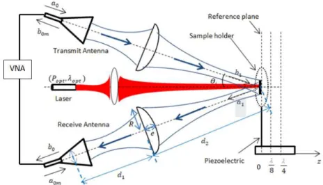
Compared to other competitive material characterisation techniques operating in guided environment, free space method fits for broadband material electromagnetic properties qualification and simultaneous optical illumination implementation needs. Furthermore, thanks to a homemade three-step calibration and a genetic algorithm-based data postprocessing technique, frequency-dependent material permittivity, permeability and conductivity parameters are obtained simultaneously with accuracy [18,19]. Schematic of the free space bistatic measurement system given in Figure2, which consists of a pair of microwave horn antennas connected to a vectorial network analyser (VNA), acting as microwave signal transmitter and receiver.
Figure 2.Schematic description of the experimental set-up.
Microwave Teflon lenses placed between antennas and the material under test (MUT), under a small signal incidence angle of 28◦ with the respect to the normal of the MUT, are added for the guarantee of microwave signal focus in a foot print at order of MUT surface dimensions and microwave signal wavelength value. These components are mandatory for occurring diffraction effects minimization at the MUT edges responsible of measurements errors.
The focusing system has been designed for a nominal microwave frequency of 50 GHz. In this configuration, the microwave lenses must be localized at a distance d1 equal to 31.85 cm from transmitter or receiver delivering a microwave signal waist of w1is equal to 1.24 cm, and at a distance d2to the MUT equal to 18.15 cm.
The lowest possible angle (θi = 28◦) is determined by the size of transmitter and receiver. This limitation is then governed by the MUT dimensions w, the distance between antennas and MUT d1+d2, as well as 3-dB angular beamwidths of each antenna in E-plane and H-plane [20]. In our configuration, the highest angle of 33◦has been calculated for a 1 cm2of MUT surface and 50 cm of distance with 20◦of antennas angular beamwidths. S-parameters measurements are performed at the distance (D=d1+d2) above the far field region limit corresponding to 50 cm at the setup lowest frequency of 40 GHz.
An optical system consisting of a LUMICS thermally-regulated cw laser diode (model:LU0808/0980/1064D100/100/100-U30AA) and a set of optical lenses is inserted between microwave horn antennas in order to realize a collimated illumination of 2.5 cm2at low incident angle on the top face of the sample in order to avoid optical back reflection signal on the laser source.
3. Calibration Technique
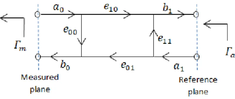
After a standard SOLT calibration procedure executed in the reference plane of the coaxial port inputs of each horn antenna, an additional homemade calibration stepis performed for measurements deembedding at the front face of the sample. This step is based on scattering parameters measurement between the two horn antennas connected to the VNA, obtained from a metallic plate used as reference short circuit and placed at three different phase references (SSS) thanks to a piezoelectric sample holder, solving errors measurements made in a quadrupole configuration as in Figure3. These error factors are attributed to multiple reflections between transmitting and receiving signals through MUT top face, as well as from non protected EM environment. As in Figure2, a0and b0coefficients correspond to incident and reflected voltage wave amplitudes from transmit and receive antennas, respectively, and b1 and a1coefficients being incident and reflected voltage wave amplitudes at a reference plane located at the top face of the MUT, respectively, as indicated in the schematic given in Figure3.
Figure 3.Quadrupole representation of microwave set-up errors.
This latter helps in the definition of the relationship between effective reflection coefficient of the MUTΓaand raw reflection coefficientΓmfrom S21coefficient measurement, through error coefficients introduction (e00, e01, e10and e11).
From equivalent circuit in Figure3, we can write that b0coefficient is equal to e00a0+e01a1, b1is equivalent to e10a0+e11a1and thatΓm,aare defined by b0,1/a0,1, respectively. Then, the corrected and raw reflection coefficientsΓaandΓm, respectively, are expressed as in (3),
Γm= aΓa+b
cΓa+1 (3)
where a= (e10e01−e00e11), b=e00and c= −e11.
To estimate the corrected reflection coefficient, it is necessary to determine the unknown parameters a, b and c, as it is reachable by testing three calibration standards at different phase reference planes delivering knownΓa.
The first calibration standard consists of a metallic sample acting as a short circuit, placed at the reference plane. The second and third calibration standards are defined by moving this metallic sample by a distance of λzm/8 and λzm/4, respectively, from the reference plane, leading to their reflection coefficient expression derived from the standard transmission line theory (4):
Γa,i = (j tan(βzmz) −1)
(j tan(βzmz) +1) (4)
With, for i = 2, z=λzm/8 and i = 3, z=λzm/4. The Equation (3) can be rewritten in analytic form
as in (5) leading to a better definition of error coefficients a, b and c.
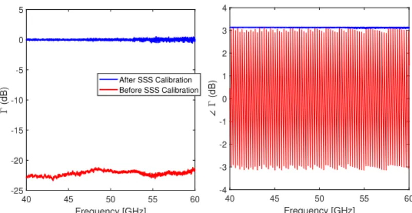
Γa,ia+b−Γa,iΓm,ic=Γm,i {i=1, 2, 3} (5) Experimental reflection coefficient magnitude and phase values of Γ of a 2 cm2 metallic sample, placed at the reference plane, are provided in Figure4in frequency, attesting calibration technique accuracy.
40 45 50 55 60 Frequency [GHz] -25 -20 -15 -10 -5 0 5 (dB) After SSS Calibration Before SSS Calibration 40 45 50 55 60 Frequency [GHz] -4 -3 -2 -1 0 1 2 3 4 (dB)
Figure 4.Experimental reflection coefficient values in magnitude and phase ofa 2 cm2metallic plate as a function of microwave frequency before and after SSS calibration (θ0=28◦and D = 50 cm) 4. Microwave Characterization of HR Silicon Material under NIR Illumination
Using the same experimental set-up, S-parameters measurements of a square HR-silicon sample of with a 2 cm2cross section and 500 µm thickness are performed at room temperature under optical power up to 10 W and wavelength of 805 nm.
Figure 5.Two independent reflection measurements.
Under light illumination, as described in Figure5, microwave incident plane wave is polarised either perpendicularly or parallel to its plane of incidence (TE or TM mode respectively) onto successively air/plasma, plasma/HR-Si and HR Si/air layers interfaces, synthesized as shunt tranverse impedances representation for each individual propagating medium.
Z2(z1) =Z0 (6)
Boundary conditions on tangential fields can be applied at z = z0. Conservation of both tangential/normal electric and normal/tangential magnetic fields through each interface may be achieved by enforcing continuity of transverse impedance Z1(TM)(z0) = ZTM2 (z0)and Z(TE)1 (z0) =
Z2TE(z0). Then, Z1(α)(z0) =χ(α)Z (α) 0 +χ(α)tanh(jkz1δ) χ(α)+Z0(α)tanh(jkz1δ) , {α=TM, TE} (7)
From (7), theoretical respective reflection coefficients Γ(TM)0 (ε∗r, µ∗r) and Γ(TE)0 (ε∗r, µ∗r) can be
established and expressed as follows,
Γ(α) 0 (ε ∗ r, µ∗r) = Z1(α)(z0) −Z0(α) Z1(α)(z0) +Z0(α) , {α=TM, TE} (8)
The free space impedance and plasma characteristic impedance, (Zα
0, χα), for the TE and TM modes are given for different angles of incidence θ0as
Z0(TM)=η0cos θ0 Z(TE)0 = η0 cos θ0 (9) χ(TM)= kz1 ωe∗r1e0 χ(TE)= ωµ ∗ r1µ0 kz1 (10) with kz1= q k2−k2
0sin2θois the propagation constant along the normal direction to the dielectric. Where k=ω√e1µ1and η0=
r
µ0
e0 is the free space impedance.
From experimental results, photoconductive material complex permittivity is extracted by using a numerical optimization procedure based on genetic algorithm [18].
0 50 100 150 200 250 300 Thickness [µm] 0 50 100 150 200 ' [S/m] 0 50 100 150 200 250 300 Thickness [µm] -50 0 50 100 150 200 '' [S/m]
Figure 6.Extraction of the HR Si substrate photoconductance∆σ (left) Real part and (right) imaginary part according to the plasma depth tpof the HR Silicon illuminated by optical power Popt = 6 W at
wavelength λ=805 nm and F = 50 GHz.
From (2), photoconductance value∆σ, attributed to the electron/hole pairs plasma layer presence induced by light absorption inside the semiconducting material, is deduced as a function of microwave frequency. In complement, from shunt impedance de-embedding calculations, a plasma profile∆σ is obtained as a function of depth inside the material, as in Figure6at a fixed microwave frequency of 50 GHz, and Figure7shows the plasma conductivity according the optical power of the NIR source and a fixed plasma depth tp= 50 µm. From fitting calculations, material absorption coefficient
α=234×103m−1, and carrier lifetime of τ=158×10−9s at 805 nm are simultaneously extracted
from measurement results.
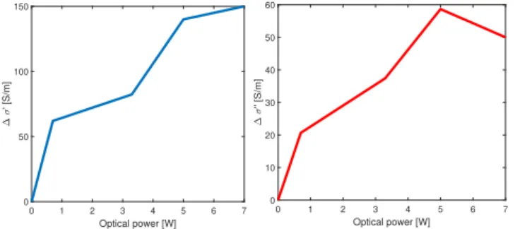
0 1 2 3 4 5 6 7 Optical power [W] 0 50 100 150 ' [S/m] 0 1 2 3 4 5 6 7 Optical power [W] 0 10 20 30 40 50 60 '' [S/m]
Figure 7.Extraction of the HR Si substrate photoconductance∆σ in (left) Real part and (right) imaginary part according to incident optical power Popat optical wavelength λ=805 nm and microwave signal
Exponential photoconductance decrease from the surface of sample is experimentally observed, on both real and imaginary parts, in very good agreement with theoretical predictions considering light penetration length at a given optical wavelength in the absorption band of the photoconductive material [21].
5. Design and Characterization of Optically-Controlled Microwave FSS
Coplanar slot based MTS structures have been designed by 550×550 µm2square metallic patches with a 100 µm gap with surrounding planar ground plane in Figure1. Metallic parts are fabricated by optical lithography of a 2 µm-thick layer of gold deposited on a 250 µm thick HR Si substrate after a SiN dielectric layer deposition and etching at edges of conductive FSS parts.
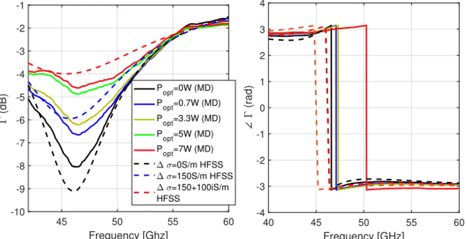
The beam spot cross section of collective optical illumination of 2.5 cm2at a wavelength of 805 nm and a maximum incident power of 10 W is applied at the top face of the MUT. In dark environment, MTS-based MUT is expected to demonstrate a microwave bandpass filtering behaviour centred at a frequency of 46 GHz. Reflection coefficient simulations have been achieved by electromagnetic (EM) full-wave analysis (Ansys-HFSS software), as shown in Figure8where conduction losses of the HR-Silicon substrate play a significant role in the frequency response.
Under optical illumination, magnitude and phase values ofΓ obtained from S21measurements reveal impedance mismatching response of MTS structures operated by light absorption through photoconductive effect operation occurring in the substrate opened ring area formed by the gap between the metallic patches and surrounding ground plane.
45 50 55 60 Frequency [Ghz] -10 -9 -8 -7 -6 -5 -4 -3 -2 -1 (dB) P opt=0W (MD) P opt=0.7W (MD) P opt=3.3W (MD) Popt=5W (MD) Popt=7W (MD) =0S/m HFSS =150S/m HFSS =150+100iS/m HFSS 40 45 50 55 60 Frequency [GHz] -4 -3 -2 -1 0 1 2 3 4 (rad)
Figure 8.Measured (MD) and Simulated (SD) magnitudeΓ(dB)and phase∠Γ(rad)values of reflection coefficient under different optical illumination power from FSS structures on HR Silicon substrate with a thickness of 250 µm.
As reported in Figure 8, dual magnitude decrease and null-phase shifting of the reflection coefficientΓ indicate the progressive device microwave response transition from a FSS to short-circuit type in the optical power range of 0 to 7 W at an optical wavelength of λ=805 nm, directly attributed to a surface impedance Zsmodification of FSS structure by optical control. Experimental results have been then validated by a complementary full-wave analysis (Ansys-HFSS software) integrating the photogenerated plasma ring layer with experimental complex data obtained in Figure1. Free carriers presence during light excitation affect the magnitude ofΓ through its real part, and the resonance frequency shift from its imaginary part as shown in Figure8. Resistive losses in silicon are responsible of the detected frequency notch as we consider a perfect dielectric substrate for dark environment representation in EM simulations.
FSS surface impedance Zsis then directly extracted from input impedance Zin=ZD.Zs/(ZD+Zs)
with ZDmodelling the impedance of the thin SiO2 dielectric layer (2 µm) covering the HR-Silicon substrate (εr =11.9 and thickness of 250 µm) inducing a resonant frequency shift betweenΓ and Zs.
45 50 55 60 Frequency [GHz] 0 100 200 300 400 500 Real (Z s ) P opt=0W (MD) P opt=0.7W (MD) P opt=3.3W (MD) P opt=5W (MD) P opt=7W (MD) =0S/m HFSS =150S/m HFSS =150+i 100 S/m HFSS 45 50 55 60 Frequency [GHz] -300 -200 -100 0 100 200 300 Imag(Z s )
Figure 9.Measured data (MD) and Simulated with HFSS (left) Real (Zs) and (right) Image (Zs) under
different optical illumination (∆σ∗) of MTS printed on HR Silicon substrate of thickness 250 µm.
As reported in Figure9, when increasing optical power, plasma conductivity enhancement∆σ tends to shunt FSS structures, where a decrease of the real part of Zs as well as a low slope of the imaginary part of the surface impedance Zsrespectively is measured. Identical frequency-dependent behaviour of Zsis observed through EM simulations by changing plasma conductivity value∆σ in the gap region.
6. Conclusions
A thin material layer characterization technique based on free space bistatic radar cross section measurements has been developed in order to extract the microwave complex conductivity and photoconductivity of a HR Silicon substrate. From this new microwave photonic set-up associated to a complementary homemade calibration technique, material absorption coefficient α , as well as carrier lifetime τ are experimentally determined. By suing this set-up, surface impedance extinction of microwave FSS structures designed, fabricated and tested on HR Si wafer, induced by a collective IR illumination have been experimentally demonstrated for the first time, in the 40–60 GHz frequency range.
These results open news routes for next generation of radar and satcom systems where ultrafast frequency agility could be operated by external optical control.
Author Contributions:Conceptualization, C.T.-C., G.P, J.C; methodology, C.T.-C., G.P., S.M., J.C.; investigation, C.T.-C., G.P., S.V.; data curation, H.K ; writing, C.T.-C., H.K.; Software, I.M. project administration, J.C.; funding acquisition, J.C. All authors have read and agreed to the published version of the manuscript.
Funding:This research was funded by THALES Defence Mission Systems, Elancourt, France.
Acknowledgments:This work has been supported by THALES Defence Mission Systems, Elancourt, France.
Conflicts of Interest:Conflicts of Interest: The authors declare no conflicts of interest. The funders had no role in the design of the study; in the collection, analyses, or interpretation of data; in the writing of the manuscript, or in the decision to publish the results.
References
1. Roy Chowdhury, D.; Singh, R.; O’Hara, J.F.; Chen, H.T.; Taylor, A.J.; Azad, A.K. Dynamically Reconfigurable Terahertz Metamaterial through Photo-Doped Semiconductor. Appl. Phys. Lett. 2011, 99, 231101. [CrossRef] 2. Berry, C.W.; Wang, N.; Hashemi, M.R.; Unlu, M.; Jarrahi, M. Significant Performance Enhancement in Photoconductive Terahertz Optoelectronics by Incorporating Plasmonic Contact Electrodes. Nat. Commun.
3. Manasson, V.A.; Sadovnik, L.S.; Moussessian, A.; Rutledge, D.B. Millimeter-Wave Diffraction by a Photo-Induced Plasma Grating. IEEE Trans. Microw. Theory Tech. 1995, 43, 2288–2290. [CrossRef]
4. Vardaxoglou, J.C. Optical switching of frequency selective surface bandpass response. Electron. Lett. 1996, 32, 2345–2346. [CrossRef]
5. Manasson, V.A. An Optically Controlled MMW Beam-Steering Antenna Based on a Novel Architecture. IEEE Trans. Microw. Theory Tech. 1997, 45, 1497–1500. [CrossRef]
6. Brand, G.F. Remote Millimeter-Wave Beam Control by the Illumination of a Semiconductor. IEEE Trans. Microw. Theory Tech. 2000, 48, 855–857. [CrossRef]
7. Li, H.; Wang, B.Z.; Zheng, G.; Shao, W.; Guo, L. A Reflectarray Antenna Backed on FSS for Low RCS and High Radiation Performances. Prog. Electromagn. Res. C 2010, 15, 145–155. [CrossRef]
8. Faenzi, M.; Minatti, G.; Gonzalez-Ovejero, D.; Caminita, F.; Martini, E.; Della Giovampaola, C.; Maci, S. Metasurface Antennas: New Models, Applications and Realizations. Sci. Rep. 2019, 9. [CrossRef] [PubMed] 9. Alibakhshikenari, M.; Virdee, B.S.; See, C.H.; Abd-Alhameed, R.; Falcone, F.; Limiti, E. A Novel 0.3-0.31 THz GaAs-Based Transceiver with on-Chip Slotted Metamaterial Antenna Based on SIW Technology. In Proceedings of the 2019 IEEE Asia-Pacific Microwave Conference (APMC), Singapore, 10–13 December 2019; pp. 69–71. [CrossRef]
10. Alibakhshikenari, M.; Virdee, B.S.; Shukla, P.; See, C.H.; Abd-Alhameed, R.; Falcone, F.; Limiti, E. Meta-Surface Wall Suppression of Mutual Coupling between Microstrip Patch Antenna Arrays for THz-Band Applications. Prog. Electromagn. Res. Lett. 2018, 75, 105–111. [CrossRef]
11. Gonzalez-Ovejero, D.; Martini, E.; Loiseaux, B.; Tripon-Canseliet, C.; Mencagli, M.; Chazelas, J.; Maci, S. Basic Properties of Checkerboard Metasurfaces. IEEE Antennas Wirel. Propag. Lett. 2015, 14, 406–409. [CrossRef] 12. Vardaxoglou, Y. Metamaterial Structures for Antenna Applications; IET Semin. Metamater. Microw. (Sub)
Millimetrewave Appl. 2008, 5–10. [CrossRef]
13. Nishimura, K.; Tsutsumi, M. Scattering of millimeter waves by metallic strip gratings on an optically plasma-induced semiconductor slab. IEEE Trans. Microw. Theory Tech. 1996, 44, 2231–2237. [CrossRef] 14. Lockyer, D.S.; Vardaxoglou, J.C. Transmission Through Optically Generated Inductive Grid Arrays.
IEEE Trans. Microw. Theory Tech. 1999, 47, 1391–1397. [CrossRef]
15. Chaharmir, M.R.; Shaker, J.; Cuhaci, M.; Sebak, A. Novel Photonically-Controlled Reflectarray Antenna. IEEE Trans. Antennas Propagat. 2016, 54, 1134–1141. [CrossRef]
16. Nishimura, K. Electromagnetic wave scattering from an optically controlled infinite periodic rectangular cavity array with an electrically short period. In Proceedings of the IEEE International Symposium on Antennas and Propagation (APSURSI), Spokane, DC, USA, 3–8 July 2011; pp. 1871–1874. [CrossRef] 17. Tripon-Canseliet, C.; Chazelas, J. Nanoscale Microwave Engineering: Optical Control of Nanodevices; Wiley
Blackwell: Hoboken, NJ, USA, 2014. [CrossRef]
18. Krraoui, H.; Mejri, F.; Aguili, T. Nondestructive measurement of complex permittivity by a microwave technique: Detection of contamination and food quality. J. Electromagn. Waves Appl. 2017, 31, 1638–1657. [CrossRef]
19. Fenner, R.A.; Rothwell, E.J.; Frasch, L.L. A Comprehensive Analysis of Free-Space and Guided-Wave Techniques for Extracting the Permeability and Permittivity of Materials Using Reflection-Only Measurements. Radio Sci. 2012, 47. [CrossRef]
20. Joseph, J.C. Multiple Angle of Incidence Measurement Technique for the Permittivity and Permeability of Lossy Materials at Millimeter Wavelengths. Master’s Thesis, Air Force Inst. Technology, Wright-Patterson Air Force Base, OH, USA, 1986; pp. 29–36.
21. Sauerer, B. Optically CW-Induced Losses in Semiconductor Coplanar Waveguides. IEEE Trans. Microw. Theory Tech. 1989, 37, 139–149. [CrossRef]
© 2020 by the authors. Licensee MDPI, Basel, Switzerland. This article is an open access article distributed under the terms and conditions of the Creative Commons Attribution (CC BY) license (http://creativecommons.org/licenses/by/4.0/).