Università degli Studi di Catania
Dottorato di ricerca in scienza e tecnologia dei materiali – XXVII Ciclo
Stefano Boscarino
Tutor: Prof. A. Terrasi
Supervisor: Dr. I. Crupi
Coordinatore: Prof. M. Grimaldi
Ultra-thin Transparent Electrodes for
U
NIVERSITÀ DEGLI
S
TUDI DI
C
ATANIA
Dottorato di Ricerca in Scienza e Tecnologia dei Materiali - XXVII ciclo
Stefano Boscarino
Ultra-thin Transparent Electrodes for
Energy Applications
Tutor: Prof. A. Terrasi Supervisor: Dr. I. Crupi
Coordinatore: Prof.ssa M.G. Grimaldi
COVER
CENTER:
Cross section scanning electron microscopy image of an AZO/Ag/AZO multilayer 100nm thick. The inset is the output of the software used to estimate the thickness of the Ag intralayer (10nm).
LEFT:
Plane view scanning electron microscopy image of an AZO surface layer deposited by RF magnetron sputtering
RIGHT:
Picture of a flexible, transparent and conductive AZO thin-film deposited on plastic substrate.
Ultra-thin transparent electrodes for energy applications
Stefano Boscarino
Ph.D. Thesis, University of Catania Printed in Catania, December 2014
Gli spiriti liberi vivono di un moderato scetticismo, amano la vita, non disprezzano la morte, seguono la ragione, non si lasciano ammaliare dagli idoli della razza, della nazione dell’autorità, del potere o profitto, dell’appartenenza ad una chiesa, ad un partito o ad una accademia, coltivano le virtù etiche della temperanza, della tolleranza, della lealtà e della solidarietà tra gli uomini, rispettano la natura senza idolatrarla, praticano la cultura del dare di contro a quella dell’avere, della collaborazione di contro a quella della competizione e della sopraffazione dell’altro, lottano per le cose giuste, cercano il vero, sono innamorati del bello, nutrono il sentimento di una sana speranza senza il mito del progresso lineare, continuo ed infinito
Contents
Motivation ………...i
Outline of the thesis ... ii
Chapter 1 Transparent conducting materials ... 1
1.1 Brief history of TCOs ... 2
1.2 Basic material physics of TCOs ... 5
1.2.1 Band structures ... 6
1.2.2 Electrical transport in n-type TCOs ... 8
1.2.3 Optical properties ... 14
1.3 Development of alternative transparent electrodes ... 19
1.3.1 Multilayered structures ... 19
1.3.2 Emerging nanomaterials ... 21
1.4 Industrial applications ... 27
1.4.1 Solar energy ... 28
1.4.2 Towards transparent electronics ... 31
Chapter 2
Al-doped ZnO ... 38
2.1 AZO deposited by RF magnetron sputtering………..………39
2.2 Material Characterization ... 44
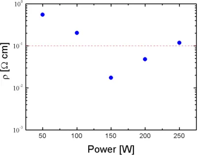
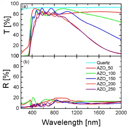
2.2.1 Influence of RF power ... 44
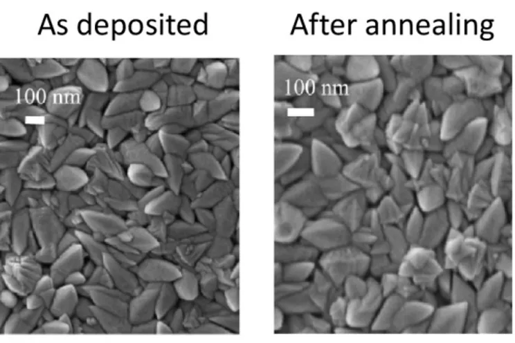
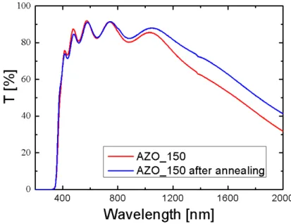
2.2.2 Effect of post deposition thermal treatment ... 57
2.2.3 Influence of the substrate temperature ... 61
2.3 Ion Implantation ... 67
2.3.1 O+ ion irradiation of AZO ... 68
2.3.2 Ar+ ion implantation of AZO on polymer substrate... 78
2.4 Conclusions ... 81
References ... 84
Chapter 3 TCO/Ag/TCO ultra-thin multilayers ... 86
3.1 Materials selection ... .87
3.1.1 Silver as intralayer ... 87
3.1.2 Which TCO?... ... 94
3.2 High-performance AZO/Ag/AZO transparent electrode ... 99
3.2.1 Appropriate Ag thickness ... 100
3.2.3 Thermal stability ... 108
3.3 TCO/Ag/TCO ... 111
3.3.1 ITO and AZO: a comparative investigation ... 112
3.4 Conclusions ... 119
References ... 121
Chapter 4 Laser scribing processes on AZO/Ag/AZO ... 124
4.1 Laser application in thin film solar cells ... 125
4.2 P1 on AZO/Ag/AZO…… ... 128
4.2.1 Laser-induced structural modifications ... 130
4.2.2 Electrical insulation ... 133
4.2.3 Heat transfer: model and analysis ... 135
4.3 Conclusions ... 140
References ... 142
Appendix: Synthesis and characterization details ... 143
Curriculum Vitae ... 175
i
Motivation
Due to the unique feature of being contemporarily optically transparent and electrically conducting, Transparent Conductive Oxides (TCOs) play a fundamental role in many technologies: communications, information, energy, buildings [1-3]. Up to now, the most diffused material in the TCO’s family was indium tin oxide (ITO), especially for large-area applications such as flat panel displays. Recently, the increasing expansion of the display market and, even more, of photovoltaics, are endangered by the scarcity and rising price of indium. This is one of the reasons and a strong motivation for searching alternative transparent electrodes, not necessarily oxides, to replace ITO. Moreover, in order to meet the expectations for the growing demand and lower production costs for photovoltaic and electronic applications, new TCOs, or equivalent materials, must be abundant, not expensive and very thin, so to be suitable for flexible electronics [1-3].
Among new transparent electrodes candidates, Aluminium-doped zinc oxide (AZO) films and very thin multilayers of AZO/Ag/AZO have emerged as a very promising alternative [2, 3]. In particular, AZO films are Indium-free and show electro-optical properties comparable to ITO films of the same thickness (typically 700-900 nm for industrial applications), especially after thermal annealing at 250 °C. On the other hand, AZO/Ag/AZO multilayer structures, 10 times thinner than ITO or AZO single layers, show very high transparency and low resistivity even at room temperature. Replacing thick TCO layers with thin TCO/Ag/TCO multilayers would produce great benefits in terms of material consumption, cost, toxicity and flexibility (a mandatory point for the development of the electronics on plastic). In this context, it is important the study and understanding of the fundamental properties of these materials, the process conditions and post fabrication treatments to optimize their application to different fields. Transparent conductive materials are known
ii
since about 100 years and represent one of the strategic topics for the actual industrial research, but still many fundamental properties and mechanisms need to be clarified and explained.
Outline of the thesis
Aim of this work is the fabrication, processing and characterization of ultra-thin AZO and TCO/Ag/TCO transparent electrodes. The study focused on the optimization of structural, optical and electrical properties for application in photovoltaics. The thesis is organized as follows.
Chapter 1 introduces Transparent Conductive Oxides (TCOs) and
covers the conventional materials history, properties and market. In particular, it gives a detailed description of the energy band structure and doping processes. After the state of the art of standard and industrial TOCs, new materials are also discussed, highlighting limits and potentialities for application in solar energy and other technological contexts.
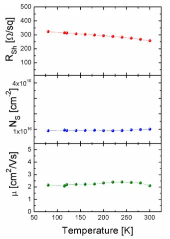
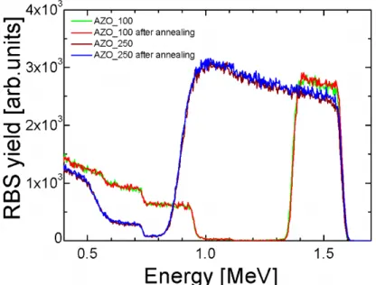
Chapter 2 is devoted to the processing and characterization of AZO films grown by RF magnetron sputtering. It starts with a comprehensive and detailed study about sputtered thick AZO films on glass substrates, focusing on the influence of sputtering process parameters, i.e. power, temperature substrate, and thermal treatment (during or after the deposition) on the film properties. A strong correlation between the deposition conditions and AZO film properties was observed: a particular set of parameters gives the lowest resistivity, the highest transparency and crystalline quality. Moreover, a thermal treatment after (200 °C) or during (up to 300°C) the deposition leads to a slight improvement and worsening of the electro-optical properties of AZO, respectively. After the work on thick AZO, we report the modification of optical, electrical and structural properties of
very thin films (60 nm) upon ion irradiation with different ion type (O+ or Ar+
iii
3x10¹⁶ ions/cm2), before and after thermal treatments up to 400°C. The
experimental data highlight the structural improvement due to ion irradiation, the strong decreases of the electrical resistivity for O+ beams
passing through or for Ar+ implanted within the AZO films. Only when O+
was implanted within the AZO, the structural improvements were accompanied by a huge increasing of the electrical resistivity, demonstrating the main role of oxygen in the activation and deactivation of the doping. Most of observed effects on the structural and electrical behaviors were very similar to those obtained after a thermal treatment up to 400 °C, without ion irradiation, so that we propose the ion beam processing as a good alternative to thermal treatments for plastic substrates.
Chapter 3 treats of very thin TCO/Ag/TCO multilayer structures grown by RF magnetron sputtering. Synthesis and properties of AZO/Ag/AZO multilayers as a function of Ag film thickness, with a fixed AZO thickness (~20 nm), are investigated. The best structure was shown to have a 9.5 nm Ag film as mid-layer, while thermal stability analysis demonstrated an excellent behavior of the AZO film as a barrier to Ag diffusion. Then, we studied multilayers with fixed Ag thickness, but different combinations of AZO and ITO as top and bottom TCO layers. The multilayered structure has shown better performances when the top and bottom TCOs are of different type, with the possibility of tuning the reflectivity in a proper range of wavelengths.
Chapter 4 describes the compatibility of the AZO/Ag/AZO multilayers with one of the most important steps for the implementation in thin film photovoltaic technology: laser scribing. A crucial aspect in the fabrication of solar panels is the patterning and electrical insulation of solar cells. Laser scribing of thick TCO films, thin amorphous Si layers and metallization layers are standard processes in the photovoltaics industry. AZO/Ag/AZO multilayers must be able to guarantee the same level of reliability under laser scribing processes. In our study, we used a single nanosecond laser pulse to irradiate ultra-thin multilayers deposited on glass. We
iv
resistance in the insulated region of AZO/Ag/AZO is enhanced by 8 orders of magnitude compared to thick single AZO, currently used in thin film sola cell. In particular, the thermal behavior, simulated using a finite element approach, shows that the silver intralayer plays two key roles on the scribing process, by increasing the maximum temperature reached in the structure and fastening the cool down process.
Finally, we decided to describe all growth, processing, analysis techniques and equipment in the appendix at the end of the thesis.
References
[1] D.S. Ginley, H. Hosono, D.C. Paine, Handbook of transparent
Conductors (Springer-Verlag, 2010).
[2] K. Ellmer, Nature Photonics 6, 809-817 (2012).
Chapter 1
Transparent conducting materials
This chapter presents an overview of the literature on transparent conductive materials. These electrodes, exhibiting both transparency and electronic conductivity simultaneously, found wide spread use in portable devices, flat-screen displays, low-emittance windows, flexible electronics and solar cells.
This chapter begins with a brief introduction on the history and the market of transparent electrodes, followed by a description of the structural, optical and electrical properties of the most commonly transparent conductive oxides (TCO) based on binary compound, such as ZnO, In2O3 and
SnO2. Then, the development of alternative transparent electrodes, ranging
from multilayer structure to nanomaterials based on carbon or metal, s over the last few years, will be presented. Finally, several of the conventional and emerging applications of TCO are described along with the additional features request behind the high electrical and optical transparency for their industrial applications.
Chapter 1: Transparent conductive materials
2
1.1
Brief history of TCOs
Transparent conductive oxides (TCO) are a unique class of materials showing the coexistence of good electrical conductivity, like metallic materials, and wide optical transparency, like insulators.
These materials have a long history of development, since the beginning of the twentieth century (1907), when Bädeker, for the first time, reported CdO thin-film, yellowish in colour, which was optically transparent and electrically conducting [1]. Since then, many metal oxides have emerged
as important transparent electrodes: tin oxide (SnO2), zinc oxide (ZnO) and
indium oxide (In2O3). After the second world war, due to the birth of the
electronics industry, SnO2 thin film were investigated for many
optoelectronics applications such as antistatic windows and heated windows. The broad industrial application of TCO materials began at the end of 1960, when In2O3 was used in low-pressure sodium lamps in order to
increase the lamp efficiency. It continued around 1970 with the advent of flat-panel display technology, when ITO (tin-doped indium oxide) became the most commercially material for transparent electrode, up to the present with the “green” technology (organic light-emitting diodes (OLED), low-ε saving energy window and photovoltaic applications) [2].
Histrorically, TCO composition is based on five set of binary compounds (see Fig.1) which, by doping on purpose, become conductive keeping high transparency in the visible wavelength range; this characteristic will be discussed into detail in the next paragraph. Although many transparent conductive oxides have been known for more than 50 years, for
instance undoped and impurity-doped SnO2, ZnO and In2O3 , ITO has been
the most studied and refined [3], due to the highest transparency for visible light combined with the highest electrical conductivity. Unfortunately, the persistent increasing of optoelectronic devices requiring one or more transparent conductor layers and the expanding use of ITO for the production of this layers is endangered by two key material issues about indium [1-4]:
Chapter 1: Transparent conductive materials
3
1) Scarcity of indium that leads to a dramatic price increasing.
2) Indium toxicity and the ceramic nature of ITO that makes it an easily
damaged layer.
Figure 1: Composition space for conventional TCO materials
This resulted into an increasing research activity on alternative materials in order to search a good replacement to ITO for transparent electrodes. Thus, the field of transparent electrodes has exploded, including new n-type materials (amorphous TCOs), composite TCO materials, the synthesis of p-type materials as well as metal, graphene, polymer and carbon nano-composites transparent electrodes materials [4-6]. Some of them will be discussed in detail in paragraph 1.3. It is important to highlight that, although other transparent conductive oxides have been known for more than 50
years, for instance impurity doped- SnO2 and ZnO, only the strong research
efforts in the last decade allowed to gain a widespread attention. Especially, impurity doped-ZnO, after the steep increase in the use of thin film solar cells to produce “green” energy, have gained interest due to abundant, non toxic and not expensive elements.
At the present, Fig.2, the transparent electrode industry is dominated by just a few TCO materials based on binary compound, and the main
Chapter 1: Transparent conductive materials
4
closely followed by the rapidly growing photovoltaics industry [3]. While the penetration of these new transparent electrodes into applications is froseen for the next 10 years [7].
Figure 2: Market of transparent conductive materials.
Due to the advent of new technologies, such as e-paper, organic light emitting diode (OLED), organic solar cells, and the emerging areas of electrochromic windows and transparent electronics, the market is fastly being transformed. New applications and trends are also changing the required features, extending them beyond the combination of high conductivity and transparency. This is because each application presents several trade-offs between cost, conductivity, transparency, flexibility, pattering, etc. The key drivers are market tendencies towards low cost, large-sized devices, low power consumption, thinness, robustness and/or flexibility, patterning easiness and simplified value chain [7, 8].
Though it is clear that transparent conductive oxide and transparent electrodes are a developing field, it is no clear which of these new and
M a rk e t b y t e ch n o lo g y t y p e U S $ m il li o n s year
Chapter 1: Transparent conductive materials
5
“rediscovered” transparent conductive oxide, and emerging materials will become the dominant player replacing ITO, also beacuse this multiplicity of options also give rise to market uncertainty and confusion. However, it is assured that the market of transparent electrodes will continue to grow and these materials will find room in new field and niches marketplace [1-8].
1.2
Basic material physics of TCOs
As previously stated, TCOs offer the remarkable combination of high optical transparency and electrical conductivity. These two properties are usually decoupled, like in metals which have optimum electrical conductivity but totally reflect and absorb the sun light, or in insulators which are high transparent (e.g. glasses) to the sun-light but show very high electrical resistivity. For industrial applications, the electrical resistivity of a TCO should
be ~10-4 Ωcm or less along with an optical band gap higher than 3.1 eV to
guarantee an optical transmission of the light, in the visible range, up to 90 % [9].
Since commercially relevant TCOs are only n-type, while the research on p-type TCOs has begun in recent years, in this paragraph we provide a brief summary of the unique opto-electronic properties of n-type TCOs.
Here we present the fundamentals of physics of TCOs, centred on the structural properties and nature of doping processes by which is possible to control their electrical properties. Moreover, it will be shown how the optical properties are related to the free carrier concentration due to the doping; both the band-gap energy and the plasma wavelength change with the carrier density.
Chapter 1: Transparent conductive materials
6
1.2.1 Band structures
TCOs are wide band gap semiconductor oxides with an optical band
gap energy, Egap, higher than 3 eV, so having a material transparent from near
UV to near infrared. The high conductivity required for their application as transparent electrodes is due to the presence of free electrons. This can be achieved in TCO by two different ways: intrinsic defects or incorporation on purpose of extrinsic dopants. Defects and dopants produce shallow donor levels that act as a source of electrons for the conduction band. If a very large concentration of doping is achieved, the Fermi level penetrates the conduction
band and the material starts to act more like a metal than as a semiconductor. In this case, the material is called degenerate semiconductors. Fig.3 shows an illustration of the band structure of an n-type TCO, which leads to the remarkable combination of high visible transparency and conductivity. Metal oxides such as ZnO, In2O3, SnO2, with an optical
band-gap higher than 3 eV are very suitable as transparent electrode. These oxides are insulators at room temperature and in the stoichiometric composition but, as said above, they can become conductive because of defects and impurities. Native point defects, like oxygen vacancies and/or interstitial metal atoms, can be formed during the deposition process, creating a non-stoichiometric material, while extrinsic doping can be achieved by introducing a metallic element, with the oxidation number +3, on substitutional lattice sites, or halogens with the oxidation number -1 on oxygen position. Doping with non-metallic elements is also common [2, 3, 9, 10], table 1.
Figure 3: Schematic energy band structure of a degenerate TCO
Chapter 1: Transparent conductive materials
7
Materials Dopant or compound
SnO2 Sb, F, As, Nb, Ta
In2O3 Sn, Ge, Mo, F, Ti, Zr, Mo, Hf, Nb, Ta, W
ZnO Al, Ga, B, In, Y, Sc, F, V, S, Ge, Ti, Zr, Hf
CdO In, Sn
Ga2O3
ZnO-SnO2, Zn2SnO4, ZnSnO3
ZnO-In2O3 Zn2In2O5, Zn3Sn2O6
In2O3-SnO2 In2Sn3O12
CdO-SnO2 Cd2SnO4, CdSnO3
CdO-In2O3 CdInO4
MgIn2O4
GaInO3, (Ga,In)2O3 Sn, Ge
CdSb2O6, Y
Zn-In2O3-SnO2 Zn2In2O5-In4Sn3O12
CdO-In2O3-SnO2 CdIn2O4- Cd2SnO4
ZnO-CdO-In2O3-SnO2,
Table 1: TCO semiconductors for thin-film transparent electrodes
It is well known that intrinsically doped metal oxides exhibit poor electrical properties and are unstable when used at higher temperature. These issues make them not well suitable for practical transparent electrodes [3]. Therefore, for practical use, we will see that TCOs thin film are principally n-type extrinsic doped wide gap semiconductors as reported in table 2 [10]. These doped-metal oxides fall into two of the four families that historically dominates the field of transparent conductive oxides. These families can be defined by its structure type as given in table 1 [11]. The first family is n-type, related to zinc oxide, where positively-charged Zn atoms are tetrahedrally surrounded by oxygen atoms. ZnO metal oxide is the only one known to have this coordination. In the second family, the larger of TCOs, cations (Sn4+, In3+,
etc.) are arranged in octahedral coordination; they also show an n-type behavior. Moreover, they are predominantly ionic bonded, with the exception of ZnO, a mix of ionic and covalent bond [12].
Chapter 1: Transparent conductive materials
8
Structural feature Carrier type Examples
tetrahedrally-coordinated
cations n-type ZnO
Octahedrally-coordinated
cations n-type
CdO, In2O3, SnO2, In2O3, CdIn2O4, Cd2Sn2O4, etc.
Linearly-coordinated cations p-type CuAlO2, SrCu2O2, etc.
Cage Framework n-type 12CaO-7AI2O3
Table 2: Cation coordination and carrier type of TCO materials
The third family is the only one showing a p-type character (electrical conduction due to holes) which has cations linearly coordinated to oxygen. Generally TCO are n-type because of the iconicity of the metal oxide, which leads to a broadly conduction band and a strong localizations of the holes at the valence band edge. Hosono and co-workes [3] designed a strategy to introduce covalency bond and to induce the formation of an extended valence band structure. This strategy was based on selected elements
synthesized into the ABO2 delafossite structure were A can be Cu or Ag and
B can be Al, Ga, Sc. Finally, in addition to the conventional TCO discussed above, another novel class of unconventional oxide based transparent electrodes, the cage-structure oxide 12CaO·7Al2O3 is also listed. It also shows
an n-type behaviour.
1.2.2 Electrical transport in n-type TCOs
In order to understand the electrical properties of a n-type TCO, we
can consider the schematic energy-band diagrams, reported in Fig.4, for In
2-xSnxO3, where x is the tin atomic percentage, corresponding to two opposite
Chapter 1: Transparent conductive materials
9
Figure 4: Schematic energy-band model of SnO2 doped In2O3 for small and large amount x of
extrinsic doping.
Since tin is a tetravalent metal (Sn4+), substituting In3+ by Sn4+ provides a free
electron to the conduction band. The doping process can also be affected by point defects, like oxygen vacancies (Vo). For each Vo (i.e a missing O2-) , the
In3+provides two electrons to the 5s conduction band, which means that
each Vo forms a shallow double donor state with an ionization energy close
to the conduction bans. These point defects have got low energy of formation and good stability, explaining why oxygen sub-stoichiometric material is preferred.
On the left side of Fig.4, for low amount of doping x, we can observe a
direct optical band-gap, Egap, of about 3.75 eV, between the empty
conduction band, formed by Indium 5s orbitals, and the full valence band
formed by oxygen 2p6 and indium 3d10 orbitals. The 2p orbitals are very low
in energy compared to 5s orbitals, explaining why a large band gap can be obtained in the intrinsic stoichiometric oxides. Moreover, it displays the
shallow donor states Sn3+ and V
Chapter 1: Transparent conductive materials
10
band energy. While, in the right side of Fig.4, for high doping, we observe a composition-induced transition from non-metallic to metallic type conduction: the conduction band is filled with delocalized electrons coming from the shallow state. The transition from insulating to metallic state of the materials is described by the Mott transition [14, 15], which takes place above a critical electrons density nc (at T = 0 K) given by:
= 0.26 ± 0.05 (1)
with =
∗ the effective Bohr radius, where ε0 and εm are the permittivity of the free space and of the host lattice, respectively, and mc* is
the effective mass of the electron in the conduction band. Collected data from the literature [13, 16] suggest that the effective mass of electron in In2O3 is about a third of the electron mass, m0, of the hydrogen, i.e. mc*≈0.35
m0, and εm≈ 4. Using these values, we obtain aH ≈1.3 nm and consequently a
critical electron density of about 6x1018 cm-3. Usually, the electron density in
TCOs is above (up to 1021 cm-3) this Mott critical density value, so it justifies
the transition from insulator to metallic behavior in the transparent conductive oxides. The schematic representation in Fig.4 is valid for most binary metal oxide wide bandgap semiconductors; e.g. in ZnO the conduction band is also composed of s-like states of the cation (Zn 3s level) while the valence band is composed of O 2p and Zn 3d levels [17].
Once understood how we can increase the conductivity without degrading the transparency in TCOs materials, we can move into the transport theory within the framework of n-type degenerated semiconductors. The electrical properties of TCO can be well explained using the simple Drude free-electron theory [3, 18]. For carrier concentration n
higher than nc, one can consider having a full valence band and a parabolic
band partially filled by a free electrons gas up to the Fermi energy: = ∗ .
Chapter 1: Transparent conductive materials
11
In the Drude theory, the differential equation of motion of the electrons as a function of the time and electric field is:
( )= ( ) − ( ) (2) ( ), e and are the electron’s momentum, elementary charge and relaxtion time, respectively, and ( ) is the electric field. The relaxtion time is the interval of the time between successive random collisions of the electrons. Since we assume the case of steady state, the electron emerges from a collision in a random direction and the average electronic velocity is given by: < >= = (3) Where m and are the free electron’s mass and mobility, respectively. In general, taking into account that electrons are not totally free in the materials, we replace m with the effective-mass m*. The concept of effective-mass arises because the electrons inside a crystalline (atoms of the material arranged in a lattice) are subjected to others forces, beyond the external electric field, that act to “alter its mass”. If n electrons per unit of
volume, in presence of a electric field , all move with velocity < >, then
the current density is = < >. According to the Ohm’s law:
= = = < >= (4) where the conductivity, σ is given by:
= (5)
with = ∗ directly proportional to the electron relaxation time and
Chapter 1: Transparent conductive materials
12
The crucial requirement for a transparent electrode is an electrical conductivity as high as possible. The best strategies to maximize the conductivity in TCO materials are to increase the electron density and/or the mobility. Very high electron density (or doping), as we will discuss in detail in the following sub-paragraph, can be deleterious because it decreases the visible wavelength transparency; moreover n and µ are correlated so, behind a certain electron density value, the electron mobility is strongly reduced due to scattering of electrons with ionized impurities [9]. Therefore, it seems that the best strategy to increase the conductivity is to limit the electron density n while increasing the electron mobility µ. As mentioned earlier, mobility
depends on effective-mass, m*, and relaxation time, τ, which, in turn,
depends on the average velocity and mean free path λe of the electron. These
parameters in TCO are limited by several scattering processes [2, 3, 17] such as:
• Ionized Impurity scattering: the coulomb interaction between the
ionized impurities (intrinsic and/or extrinsic donors) and the free electrons.
• Grain boundary scattering: they are especially present in
polycrystalline films, disturbing the translation symmetry of the crystal and thus causing scattering. Grain boundary diffusion can be significant if the grain size, D, is comparable to the mean free path of the electron λe.
• Optical and acoustic phonons scattering: the former is the
interaction between electrons and the electric field induced by electric polarization associated with the lattice vibration at optical frequencies. While the latter is the interaction between the electrons and the lattice deformations corresponding to pressure waves.
• Piezoelectric scattering: interaction between electrons and the
electric field produced by the strain associated with acoustic phonons.
Chapter 1: Transparent conductive materials
13
According to the Matthiessen rule [19], the total probability for an electron to be scattered in the unit time is the sum of the probabilities of the independent scattering processes:
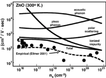
= ∑ → = ∑ (6) Therefore, the dominating scattering process will limit the electron mobilty. As we can see from Fig. 5 [18], in the case of impurity doped ZnO (similar for
impurity-doped In2O3 and SnO2), at room temperature the dominating
scattering process in TCO, (degenerately doped metal oxide, n>1019cm-3)
which limits the mobility, is the ionized impurity scattering.
Figure 5: Influence of scattering processes on ZnO mobility, at room temperature, as a function of carrier concentration
Taking into account only this scattering mechanism and very high electron density, theoretical study established an absolute limit to the TCO conductivity of about 105 S cm-1 [20, 21]. About one order of magnitude
Chapter 1: Transparent conductive materials
14
Another parameter controlling the mobility is the effective mass: the smaller the effective mass, the higher the mobility is. The effective mass is considered an intrinsic parameter of a material that depends on its composition, however the effective mass has also a strong dependence on the electron concentration by means of the dispersion relation E(k) [22]. The reciprocal of the effective mass in proportional to the curvature of the energy band, which in turn depends on the doping concentration. Therefore, we can conclude that the best strategy to achieve high conductivity is to maximize the product n µ, eq. 5, by acting on these scattering mecchanisms, which dominate the mobility at not very high doping concentration.
Finally, the electrical performances of a thin film are expressed by the electrical resistance offered by a square shaped sample of homogeneous
material having a thickness d, known as sheet resistance =
(Ω/square). The sheet resistance depends on the resistivity and thickness, while it does not depend on the film dimensions (length and width). Generally, a certain sheet resistance is needed in order to meet the electrical functionality of a specific application. For instance, a sheet resistances of 400-700 Ω/sq in touch screens, and below 10 Ω/sq in flat panel display and thin film solar cells [23].
1.2.3
Optical properties
As mentioned above, besides high electrical conductivity value ~ 105 S
cm-1, from a practical point of view, TCO should have a wide transmission
window in the near ultraviolet-visible-near infrared region. The optical transmission of a material is defined as the ratio between the incoming light intensity and the transmitted light intensity averaged over the wavelenght range. Figure 6 shows the typical reflection, transmittance and absorption spectra of a TCO film, with a high transmission in the visible range [1]. The width of the transmission window is controlled by two different phenomena taking place in the near ultraviolet and infrared regions.
Chapter 1: Transparent conductive materials
15
Figure 6: Optical spectra of typical transparent conductive oxides (ZnO)
In the near IR, for wavelengths > ~1000 nm, the decreasing of the transmission and the corresponding increasing of the reflection are due to the oscillations of the electrons in the conduction band, known as plasma oscillations, and intra-conduction band transitions. The characteristic
frequency, known as plama frequency ωp, can be predicted using the
Maxwell’s equations of the electromagnetic theory within the framework of the Drude model: the free electrons in the conduction band are assumed to oscillate in response to the electric field components of the electro-magnetic
field, i.e the light [3, 18]. We can define ωp starting from the Drude form of
the frequency-dependent dielectric function ε(ω) of the material: ( ) =
+ , with the real part and imaginary parts given by:
Chapter 1: Transparent conductive materials
16
where τ is the time between two successive collisions of the electrons in the
lattice, σ = ∗ the d.c. conductivity, ε∞ the high-frequency permittivity, εo
the vacuum permittivity and ω the angular frequency of the electric field.
Assuming that ≫ 1, the condition = 0 defines the plasma
frequency of a TCO materials which is given by:
= ∗ (8) As we can see, there is a negative correlation between the electron density
and the wavelength position in the IR region ( ∝ ) where the free carriers
start to reflects and absorbs the incident electromagnetic wave. It is important to point out as for most TCO materials, due to their electron concentration, the plasma frequency falls in the near-infrared part of the spectrum. Therefore, if we increase by doping the number of electrons in the conduction band, the conductivity increases but also the IR absorption edge shifts towards shorter visible wavelength, narrowing the transmission window.
Across the visible range (400 – 800 nm) of the solar spectrum, the transmission reported in Fig. 6 is characterized by a transparency up to 90% and oscillations due to the thin film interference effects. The high transparency is correlated to the schematic electronic structure previously shown, in which p and s orbitals produce a completely filled lower valence and an upper conduction band separated by large band-gap energy, more than 3 eV, which makes the material transparent in this wavelength range.
Moving to shorter wavelengths, in the near UV range, we observe an abrupt drop in the transmission at around ~300 nm. The TCO material becomes opaque due to the absorption of UV photons: the photon energy is higher than the band-gap energy and photons are absorbed.
As above mentioned, mostly of TCO are n-type degenerate semiconductors. Due to the high doping, the Fermi level shifts into the
Chapter 1: Transparent conductive materials
17
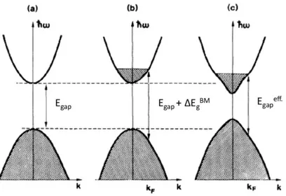
conduction band, hence the lowest energy states are occupied by free electrons, Fig. 7(a).
Figure 7: Burstein-Moss and Band-gap renormalization band-filling effect contributions to the Egap.
Now, the photon energy required to promote an electron from the the valence band to the first available unoccupied state in the conduction band will be higher than the original band-gap energy, Fig. 7(b). The wider band optical gap is consequence of Pauli's exclusion principle that forbids excitation into occupied states in the conduction band. This
doping-dependent Egap shift is known as Burstein-Moss effect [24], responsible for
the band-gap energy widening when increasing the doping concentration. The effective energy band-gap between the top of valence band and lowest empty state in the conduction band (both assumed parabolic) is given by:
Chapter 1: Transparent conductive materials
18
In this formula Egap is the intrinsic bandgap of the material, m* the effective
mass of the electrons, and n the electron concentration. Here we have a direct relationship between the carrier concentration (doping) and the UV
absorption edge, ∆ ∝ . By increasing the carrier concentration, we
increase both the conductivity and the trasmission windows, due to the shift of UV edge towards shorter wavelenght. This feature does not correctly describe the experimental data, because we employed a rigid band model, which takes into consideration only the shift of the Fermi level into the conduction band. Due to the high electronic density we have to take into account the many-body effects (electron-electron and electron-impurity scattering), which leads to a band-gap narrowing [25, 26], Fig.7(c). Moreover, we can also observe a modification in the shape and curvature of the conduction band, which can modify the effective mass of the electrons. The theory, combining the many-body and Burstein-Moss effect, provides an effective band gap energy of:
. = + ∆ − ℏ∑ (10) The term ћΣ in the equation represents the self energies due to many-body effect, causing a band gap narrowing that counteracts the Burstein-Moss effect. In particular, as demonstrated by Sernelius et al., for highly-doped ZnO this theory was found agree well with the experimental data [26].
In conclusion, the ideal TCO would be fully transparent in a wide range of wavelengths as well as have metal-like conduction but, as we have seen, the electrical and optical properties are intrinsically interconnected; therefore, TCO optimization needs the ability to trade-off carrier concentration against mobility to increase transmission window while maintaining high conductivity.
Chapter 1: Transparent conductive materials
19
1.3
Development of alternative transparent
electrodes
The best and most commercialized transparent electrodes are based on impurity-doped metal oxide, of which the most common is ITO. The key material issues related to indium and the persistent increasing in advanced devices that require transparent electrodes with higher conductivity and transparency, as well as other features such as lower cost and abundance elements, fabrication at low temperatures and plastic substrates, have stimulated the research, leading to many alternative and new transparent conductors.
This paragraph briefly explores the properties of these alternative transparent electrodes, principally covering multilayer structures and some of the current nano-materials coatings.
1.3.1 Multilayered Structures
Since early 1950s, very thin film of Ag, Cu or Au have been used as transparent electrode [27]. In order to achieve electrical properties very close to bulk material, the thickness of these films must be about 10 nm or more, depending on the metals, so have a continuos layer without holes or clusters. Higher thickness are even better for the electrical conductivity but, in this case, a high reflectance and absorption of the light are strong limiting factors for their application as transparent electrodes. In order to increase the transmittance trough metal films and exploit its excellent electrical properties, TCO/metal/TCO multilayer structure have emerged as a a promising alternative. Substantially, the outer TCOs act as anti-reflection coatings, so decreasing the reflectance [3]. A carefully adjustment of the refractive index and thickness in these structures can decrease the reflectance within a broad wavelength range. Usually the best electro-optical performances of a standard ITO are obtained with thickness higher than 500
Chapter 1: Transparent conductive materials
20
nm. These very ultra-thin multilayerstructures such as ITO/Ag/ITO, with 100
nm of overall thickness, can provide a significant drop in indium consumption and allow the achievement of electrical-properties comparable to single ITO. Analogous performance has been achieved with other TCO/metal/TCO, as reported in table 3 [28].
TCO/metal/TCO description substrate Rsh [Ω/sq] T [%] ITO 50 nm/Ag 8 nm/ITO 50 nm
GIO 40 nm/Ag 8 nm/GIO 40 nm ITO 37 nm/Ag(PdCu) 8 nm/ITO 37 nm AZO 40 nm/Ag(PdCu) 8 nm/AZO 40 nm
ITO 30 nm/Ag 8 nm/ITO 30 nm ZnO 57 nm/Ag 9 nm/ZnO 40 nm ITO 35 nm/Ag 10 nm/ITO 35 nm ITO 35 nm/Ag 10 nm/ITO 35 nm SnO2 45 nm/Ag 10 nm/ITO 45 nm GZO 30 nm/Ag 10 nm/GZO 40 nm ITO 30 nm/Ag 10 nm/ITO 30 nm ITO 40 nm/Ag 10 nm/ITO 40 nm ITO 45 nm/Ag 10 nm/ITO 45 nm AZO 40 nm/Ag 10 nm/AZO 40 nm ITO 50 nm/AgCu-alloy 10 nm/ITO 50 nm
ITO 50 nm/Ag 10 nm/ITO 50 nm ZnO 35 nm/Ag 12 nm/ZnO 35 nm GZO 30 nm/Ag 12 nm/GZO 30 nm IZO 30 nm/Ag 12 nm/IZO 30 nm AZO 40 nm/Ag 12 nm/AZO 40 nm GZO 40 nm/Ag 12 nm/GZO 40 nm ITO 40 nm/Ag 12 nm/ITO 40 nm ITO 50 nm/Ag 14 nm/ITO 50 nm ITO 70 nm/Ag 14 nm/ITO 70 nm IZTO 30 nm/Ag 14 nm/IZTO 30 nm
IZO 40 nm/Ag 14 nm/IZO 40 nm ITO 40 nm/Ag 15 nm/ITO 40 nm ITO 42 nm/Ag 15 nm/ITO 42 nm ITO 43 nm/Ag 16 nm/ITO 43 nm ITO 40 nm/Ag 16 nm/ITO 40 nm ITO 50 nm/Ag 17 nm/ITO 50 nm ITO 54 nm/Ag 20 nm/ITO 54 nm ZnO 50 nm/Cu 5 nm/ZnO 50 nm ZnO 30 nm/Cu 6 nm/ZnO 30 nm AZO 40 nm/Cu 8 nm/AZO 40 nm ITO 40 nm/Cu 14 nm/ITO 40 nm ITO 30 nm/Cu 16 nm/ITO 30 nm AZO 50 nm/Au 9 nm/AZO 50 nm ITO 50 nm/Au 10 nm/ITO 40 nm IZO 40 nm/Au 12 nm/IZO 40 nm
Glass Glass Glass Glass PEN Glass PET Glass Arton Glass Glass Glass Arton PET Glass Glass PET PES PET Glass Glass PES PET PPC PET Glass Glass Glass Glass Glass PET Glass Glass PEN Glass Glass Glass Glass PC Glass 15 11.3 10 10 6.8 7 10 9 7 7 6 6 6 6 5.7 5 10 7 6.9 7 6 4.3 11 6.5 5 4.2 4.2 3.3 8.9 4.4 6.7 3.5 10 10 9 6 6 12 5.6 5.5 89 92.9 89 88 85 95 77 80 85 90.7 90 87 86 85 83 88 75 87.2 84.8 82 87 89.3 81 68 86 87.7 85 85 79.4 86.5 83.2 75 83 88 84 69 88 83 72 81
Table 1: Sheet resistance (Rsh) and optical transmittance (T) values reported for several
Chapter 1: Transparent conductive materials
21
Usually, the best electrical performance of many TCOs are obtained after thermal treatment at high temperature, more than 250 °C, during or after the deposition process, which are incompatible with thermoplastic substrates. All the multilayer structures listed in table 3 have been prepared by several deposition techniques, such as sputtering and evaporation, on differnet substrates, among which PEN (polyethylene naphthalate), PET (polyethylene terephthalate) and PC (polycarbonate). The main feature of these structures is the achievement of the high visible transmittance and low electrical resistance at room temperature deposition, which offers the chance to substitute rigid glass with thermoplastic polymers as substrate. Moreover, the very thin thickness of the multilayer structure and the flexibility of the metallic interlayer assure a better mechanical stability than thicker TCO single layers [29]. From the point of view of the manufacturing, advantages like simply deposition techniques, flexibility of the material and lower production costs (plastic substrate and no thermal treatments) make multilayer structures extremely favourable in the development of low-cost, high quality, flexible electronics and photovoltaic devices. Other characteristics such as surface roughness, thermal stability [30,31] and durability against humidity and chemical agent have been evaluated by several tests [32-34], because in addition to the crucial requirements of flexibility, low cost and high conductivity-transparency these features can also be decisive for their commercial applications. Nowadays, these features allowed the use in several conventional and emerging applications such as flexible random access memories [35], organic photovoltaic devices (OPVs) [29, 36-38] and organic luminescent displays (OLEDs) [39, 40].
1.3.2
Emerging nanomaterials
Over the last years, a high level of technological abilities, from synthesis to in-depth analysis, opened the door to several emerging nanoscale materials. These new materials offer new physical properties
Chapter 1: Transparent conductive materials
22
combined with low costs, making them excellent candidates for the next generation of transparent conductors [3-6]. Here we will focus on carbon nanostructures such as graphene and carbon nanotubes, and metal nanostructures, as silver nanowire networks.
Single or multiple graphene sheets, Fig.8 (a), are rapidly emerging as transparent electrodes due to the intrinsic high in-plane conductivity and transmittance.
Figure 8: (a) Carbon atoms arranged in a graphene lattice, (b) AFM of a network of random graphene flakes.
The high conductivity in a single layer of graphene is due to the low
concentration of charge carriers and very high electron mobility, up to ~104
cm2/V s over the sheet, like a two-dimensional electron gas [41, 42]. While
the high optical transmittance is due to the low optical opacity of a single graphene layer, about 2.3%. Moreover, as predicted by Peumans et al. the sheet resistance and the optical transmittance of a large and defects-free
structure of graphene, linearly decrease with the number of layers N: Rsh~
62.4/N Ω/sq and T ~ 100 - 2.3N % [42-45], respectively.
The extensive research and the various fabrication methods developed to study and grow large, defects-free and industrially scalable graphene sheets, such as mechanical exfoliation of highly oriented pyrolytic graphite (HOPG) [46], chemical vapor deposition on Ni films [47] and solution
Chapter 1: Transparent conductive materials
23
based process [48], have drastically improved the opto-electrical properties of this material. From Rsh~2000 Ω/sq and T ~85%, to Rsh ~700 Ω/sq and T
~90% in the cases of solution and CVD processes, respectively. However, the high sheet resistance prevents their application in solar cells and flat panel display, which require a value of ~10 Ω/sq. With the goal of decreasing the sheet resistance, two main strategies are pursuited: to increase the carrier mobility synthesizing large and single sheets without defects, or to increase the carrier concentration by doping. For example, Bae et al. [4] achieved sheet resistance and optical transmission of ~30 Ω/sq & T ~90 %, respectively, growing a layer-by-layer stack to fabricate a doped four-graphene layer film by chemical vapor deposition onto Cu foil and then transferring it onto plastic substrate. For practical use, thermal [49] and mechanical/electrical stability [50] have also been demonstrated. These outstanding properties of graphene make it very attractive for applications in many fields, from flexible electronics to photovoltaics. However, large-area deposition technologies of graphene films are still in their infancy, and a main drawback is related to the higher temperature (~700-900 °C) needed to grow graphene. Moreover, instead of a single sheet of graphene, often a network of graphene flakes is synthesized, Fig.8 (b), which shows high resistivity due to the contact areas [4].
Another emerging subclass of carbon based transparent electrodes is carbon nanotubes (CNTs), cylindrical structures of carbon atoms, Fig. 9. Although the first experimental synthesis was made in the early 1990s [51], and the subsequent studies have shown amazing electrical (mobilty higher
than 105 cm2/V s), optical and mechanical properties, CNTs needed several
years to find widespread appeal as transparent electrodes due to several issues.
Chapter 1: Transparent conductive materials
24
Figure 9: Single walled CNT.
One of major factor limiting their application is the high conductivity of CNTs compared to single CNT, because the high junction resistance betweeen CNTs, typically of the order of 200 kΩ-20 MΩ, produces a drastically increasing in the conductivity. There has been much work done to increase the conductivity value, such as doping with nitric acid or using longer CNTs [52, 53], however films of CNTs still have a much lower opto-electrical performance than commercial ITO. Another impediment is related to the material synthesis. Typically, as produced CNT films consist of a mixture of both seminconducting and metalllic CNT, with the metal/semiconductor ratio influencing the opto-electrical performances. The metallic CNTs have a much higher conductivity than semiconductor ones, moreover the latter absorb light, so reducing the optical transmission. The junction resistance between two metallic CNTs is much lower than metallic-semiconductor CNTs, which form a schottky barrier, therefore the whole conductivity can be decrease if we made a film entirely of metallic CNTs [54]. Although some methods have been introduced to separate metal and semiconductor CNTs
Chapter 1: Transparent conductive materials
25
or to synthesize only metallic CNTs, these challenges are still to be won, also including large e low-cost fabrications for commerial applications.
In order to use the high conductivity of silver and also to avoid the absorption and/or reflection in the visible/NIR range, silver ultra-thin films have been replaced with silver nanowires networks [55-58]. One of the main advantages of using nanowires lies in the increased transparency, because the light can pass through the empty spaces. Another advantage is the simply and low cost solution-based synthesis, especially when they are fabricated as network of silver nanowires randomly oriented. Silver nanowire films can be fabricated either at room temperature, or at low annealing temperatures [59, 60], which make them compatible with plastic flexible substrates.
Networks of silver nanowires can achieve low sheet resistance, Rsh ~10-20
Ω/sq, and high transparency, T ~ 90 % by using pure and smooth metallic nanowires with suitable diameter and length [4]. Moreover, a denser network will result in a decreasing of the sheet resistance but also of the transmission of light, Fig.10. Recent works proved that sheet resistance and surface roughness of this mesh can be decreased by mechanical pressing, melting the nanowire junctions [59]. This network also shows the noticeable feature of scattering the transmitted light, known as haze, which is not desired for displays and touch panels but it can be very useful to increase the light absorption in solar cells. In order to decrease the haze, nanowires can be in theory made with diameters smaller than 50 nm, although, to date, the published results range from 50 to 200 nm, with a length in between 1 and 20 μm. In any case, thinner nanowires would result in a worsening of the conductivity due to the increasing of surface scattering.
Chapter 1: Transparent conductive materials
26
Figure 10: SEM images of Ag NW films with different densities. The different densities lead to different sheet resistances: (a) 100, (b), (c) 50, and (d) 15 Ω /Sq.
Although a network of silver nanowires is low cost, flexible, and shows desirable transparency and conductivity values, there are some issues that need to be addressed before these transparent electrodes can be used in commercial devices, such as the structurabilty, the long-term stability and large-scale fabrication.
In conclusion, in Figure 11 reports the best otpical (lower graph of (a)) and electrical (b), results for CNTs, graphene, silver nanowires and standard transparent electrodes, along with the luminosity function of the human eye and the spectral irradiance from the Sun under AM1.5 conditions (upper part of (a)) [2].
Chapter 1: Transparent conductive materials
27
Figure 11: (a) spectral transmission of several transparent electrodes: ITO (black line), FTO (green line), AZO (orange line) carbon nanotubes (dashed black line), silver nanowires (dotted blu line) and SnO2/Ag/ SnO2 (red line). (b) sheet resistance, Rsh, as a function of the thickness
for different transparent electrodes.
Although this new materials show a significant progress in improving opto-electronic performances, and also offer some advantages such as low costs, room temperature deposition, flexibility, etc., they still have to reach the performance of ITO and, moreover, to demonstrate the capability of large area industrial production.
1.4
Industrial applications
TCOs materials found a widespread use in many important technologies ranging from architectural (low-ε windows) to information & energy applications (e-paper, display, touch-screen, photovoltaics) [1-8]. Briefly, several of these consolidate and emerging technologies will be described in the following two sub-paragraphs.
Chapter 1: Transparent conductive materials
28
1.4.1 Solar energy
Over the last decade there has been an increasing interest in the use of photovoltaic (PV) technology as a renewable and inexpensive energy source, which has resulted in a plenty of solar cells technologies: mono and polycrystalline silicon solar cells, thin-films, organic and hybrids. While the absorber materials can vary a lot, each one with advantages and disadvantages, all photovolaic technologies use very similar geometry and operation mode [61]. The solar cells is fabricated by sandwiching the absorber materials between two electrodes (with the exception of the all back contact solar cells). One of the electrodes, "front or top" electrode, is typically a transparent conductive oxide material, and usually is placed between a transparent supporting substrate (glass) and the absorber material. The sunlight passes through the glass and TCO before it is absorbed by the active layer. The "back or bottom" electrode which is opposite to the front electrode, generally comprises a metal thin-film or alternatively a transparent conductive material. Some of the most consolidate and emerging photovoltaic devices, with the required properties of TCOs, are listed in table 4 [62].
As we can see, beyond the crucial requirements of high transmission and high conductivity, the choice of the best TCO for a specific solar cell should also be considered, along with processing, cost, material compatibility, work function and energy band alignment. In fact, for a widespread use of PV technologies, it is essential to take into account lower production cost and environmental impact. In this contest, the high price, scarcity and toxicity of In are a remarkable drawback, which endangered the expanding use of ITO and the development of In based solar cells.
Chapter 1: Transparent conductive materials
29
Cell type TCO in current use TCO needs Materials goal
Heterojunction with intrinsic thin layer (HIT)
cell
ITO
Smooth and good interfacial properties, optimum conductivity, low temperature deposition, light trapping IZO, indium-free material, ZnO Copper indium gallium selenide (CIGs) i-ZnO/Al:ZnO Inferfacial stability to CdS, Low temperature deposition, resistance to diffusion and shorting, need to make/improve the junction. Single-layer TCO to replace two layers and CdS layer CdTe SnO2 Zn2SnO4/Cd2SnO4 Stable interface to CdS/CdTe at high temperature, diffusion barrier Doping of Zn2SnOx materials, Single layer TCO
Nano-hybrid
polimer cell ZnO, SnO2,TiO2
Nanostructure with right length scale, work-function, interface with organic and correct doping level
Self-organized structures core-shell structure,
new non conventional TCOs
Grätzell cell TiO2
Nanostructure with high electron mobility
Improved TiO2 morphology and possible used of doped materials, new non-TiO2 materials Amorphous Si
SnO2,ITO and
ZnO many cells employ two TCOs
Temperature and chemical stability, and appropriate texture for both TCO
Higher conductivity, texture and ohmic contact for both TCO
Chapter 1: Transparent conductive materials
30
In the Heterojuctions with Intrinsic Thin-film layer (HIT) solar cell, Fig 12 (a), two TCO layer are employed, one for the top and one for the bottom of the cells [62,63].
Figure 12: (a) Typical configuration for HIT solar cell. (b) Schematic view of an organic photovoltaic cell using a nanostructured TCO grown on a planar TCO layer and intercalated with a conjugated polymer
.
As the lateral conductivity of doped a-Si:H layers is poor, the front of the devices must be coated with a TCO layer to transport charge to the device terminals. The front TCO also serves as an antireflecting coating in order to limit losses. Usually ITO has been used, but the low thermal stability of crystalline/amorphous structure limited the thermal treatments up to temperature value that does not allow the reaching of the ITO’s best performance. For this reason, there is an increasing interest to use amorphous IZO, which shows high quality even at room temperature deposition. This represents an important driving factor to further improve the device performances. While the other TCO acts primarily as a transparent electrode without incurring contact resistance losses.
In wafer-based and thin-film type solar cells, a specific feature, beyond high transparency and conductivity, is required for TCO: texturing. A textured surface will not only reduce reflection, but will also give a longer optical path to the light inside the absorber material (light-trapping). As a result, the incoming light will be completely absorbed during one single pass. The light scattering is usually achieved by texturing TCO substrate (before or after the deposition) by wet-chemical and lithography etching steps. Therefore, the
Chapter 1: Transparent conductive materials
31
optimization of the texturing technique can lead to an improving of the solar cells efficiency and a reduction of the absorber thickness, with strong advantages on the production costs.
In CdTe and Cu(InGa)Se2 (known as CIGS) thin film solar cells, low
temperature deposition and thermal stability after the deposition also play a crucial role for choosing the most suitable TCO. In particular, in CIGS solar cells, a three-layer TCO (CdS/i-ZnO/AZO) is used, which acts both as defect passivation layer and as transparent electrode. While in cadmium telluride solar cells, where the CdTe/CdS stack begins with TCO coated glass, the goal is to find an optimum tredoff between the resistivity value and the ability to act as barrier against diffusion during the high temperature deposition of the CdTe layer.
Transparent conductive oxides are traditionally used in devices as thin film, while hybrid and dye sensitized (Grätzel) solar cells, Fig.12 (b), require TCO materials of different type, for instance, three dimensional nanostructures like nanorods. Nanostructured TCO electrodes help to maximize the inorganic/organic interface and reduce the distance between the organic film and the TCO contact. The poor exciton and charge carrier transport in the organic layer require very short distance, less than 10 nm, between TCO and organic layer for a successful device. Additional properties of the TCO used to contact the organic layer are important, such as work function, surface morphology and chemistry. The work function must be
optimized to match the energy levels in the organic absorber material in
order to facilitate the charge collection, while the surface chemistry is critical for the charge transfer at the interface.
1.4.2
Towards transparent electronics
After the advent of flat-panel display (FPD) technology, around 1970, this field became one of the largest and fastest-growing applications of TCO. Traditionally, this role has been well performed by ITO due to its excellent electro-optical properties and the relative ease of acid etching.
Chapter 1: Transparent conductive materials
32
Briefly, in FPD each pixel consists of a layer of nematic liquid crystal aligned between two ITO thin film layers, and two polarizing filters (parallel and perpendicular) which have axes of transmission (in most of the cases) perpendicular to each other. Without the liquid crystal between the polarizing filters, due to their polarization, the light passes through the first filter but will be blocked by the second filter. Viceversa, by controlling the applied voltage across the liquid crystal layer in each pixel, we will modify the polarization of the light. Therefore, light can pass through the liquid crystall with different intensities, thus constituting different levels of gray. Generally ITO is etched as pattern of lines oriented perpendicular to each other on the two substrate, this allows addressing individual pixels by applying a voltage to the row and column lines which intersect at a given pixel [64,65]. Thus patterning of the ITO film is a crucial requirement.
Touch panels are the other devices using TCO thin film, with an exponential growth rqte. In touch screen applications, usually, very low overall sheet resistance of TCO is not fundamental, but rather the long-term post-deposition stability and mechanical durability. In this application, TCO allowed to define the x-y position on the surface of the screen, therefore a change in the resistance, either locally or globally, leads to a shift of the contact position [64, 65].
Another dominant markets for TCOs is the architectural window applications. In application such as defrosting windows, TCO coated glass is used because by applying an electrical current to the TCO layer, it warms up due to the Joule effect and prevents the condensing of the air. While in the low-ε windows the conductivity of TCO is irrelevant and they are used only for their optical properties: the high reflectivity in the the infrared spectral range. To this purpose, depending on which side the TCO layer is exposed, i.e. outside or inside the building, we can control the heat and light flux passing through the window. This feature is used to minimize air conditioning in summertime and heating in the wintertime. Fluorine doped tin oxide (FTO) is the TCO most often used in this application due to the advantages that it is inexpensive both in terms of raw material and processing .
Chapter 1: Transparent conductive materials
33
In addition to the conventional and consolidated TCO applications, there is an emerging area that could rapidly be mature and increasing the TCO use on a large scale: oxide based thin film transistor (TFTs and T(ransparen)TFTs) [3]. All TCOs discussed and employed are n-type semiconductors, however p-type TCOs have been also developed and represente an important milestone in transparent electronic, allowing frabrication of wide band-gap p-n junction. Though significant progresses have been achieved over the last ten years, further intensive research is needed because type TCOs are still a critical issues, as demonstrated by
p-type ZnO. High carrier concentration (>1019cm-3), high mobility and
persistence of p-type behaviour for long times is needed in order to win the
challenge to obtain p-type TCO with resistivity lower than about 10-3 Ωcm
[3-17]. Another important issue is the development of transparent amorphous semiconductors ([In2O3]x[ZnO]1-x;[Ga2O3]x[In2O3]1-x) discovered by the Hosono
group more than 10 years ago [66-68]. The advantages of these materials are the deposition at lower temperature (amorphous material) with respect to crystalline TCO materials and performances comparable to the TCO polycrystalline materials. Other remarkable properties are their high temperature stability and flexibility, thus allowing the use of plastic substrate. Therefore, if a pn-junction with good performance and stability is fabricated with polycrystalline and/or amorphous TCOs on plastic susbtrate by cheap deposition technique, this would be a breakthrough for flexible electronics.