0
UNIVERSITA’ DELLA CALABRIA
Dipartimento di Fisica
Scuola di Dottorato
Scuola di Dottorato “Archimede” in Scienze, Comunicazione e Tecnologie
Indirizzo
Fisica e Tecnologia Quantistica
CICLO XXVIII
Graphene synthesis by top-down and bottom-up strategies
Settore Scientifico Disciplinare : Nanotecnologia
Direttore: Prof. Pietro Pantano
Firma _____________________________
Supervisore: Prof. Lorenzo S. Caputi
Firma______________________
Supervisore: Dott.ssa Adalgisa Tavolaro
Firma______________________
Dottorando: Dott./ssa Denia M. Cid P.
Firma _____________________
Anno academico: 2014 – 2015
1
Graphene synthesis
by top-down and bottom-up
strategies
2
ABSTRACT (Italian version)
Il Grafene è un materiale che ha una struttura bidimensionale composto da atomi di carbonio disposti in una forma esagonale (simile ad un nido d'ape) a formare un film ed ha proprietà fisico-chimiche uniche, tanto che ha suscitato notevole interesse nella comunità scientifica per le sue proprietà e applicazioni. Per produrre Grafene, vengono utilizzati diversi metodi che possono essere divisi in due grandi categorie caratterizzate da un diverso approccio metodologico: l'approccio bottom-up e l’approccio top-down. In questo lavoro, saranno esplorate entrambe le vie.
Questo lavoro di ricerca ha riguardato entrambe le categorie ed in particolare, per quanto riguarda l’approccio bottom-up, saranno riportate le proprietà del grafene su una superficie di nickel monocristallino ottenuto per Deposizione Chimica di Vapori da etilene (CVD).
Nel approccio top-down, la grafite naturale è stata utilizzata per la preparazione di materiali a base di grafene ottenuto per mezzo di una preparazione innovativa.
Tutti i materiali ottenuti sono stati caratterizzati tramite spettroscopia elettronica Auger, Diffrazione di elettroni a bassa energia (LEED), Microscopia elettronica a scansione (SEM) ed a trasmissione (TEM), Spettroscopia Raman, Spettroscopia fotoelettronica a raggi X (XPS) e Spettroscopia di perdita di energia degli elettroni (EELS).
Come risultato, nell’approccio bottom- up, gli atomi di cesio restituiscono la linearità al grafene e questo si comporta come grafene quasi-libero.
Nel approccio top-down, sono stati ottenuti estesi e transparenti strati di ossido di grafene, privi di difetti. Gli strati preparati chimicamente sono stati ottenuti in forma solida e sembrano coordinare la zeolite ottenendo probabilmente, così, la necessaria stabilizzazione energetica.
3
ABSTRACT
Graphene is a two-dimensional structure arranged in a hexagonal form (similar to a honeycomb) that has unique physicochemical properties and has generated interest in the scientific community for its properties and applications. To produce graphene, several methods are used, all of them can be divided in two approaches: the bottom-up approach and top-down approaches. In this work, both routes will be explored.
In the bottom-up approach, the properties of graphene over a mono crystalline nickel surface obtained by chemical vapor deposition (CVD) will be studied.
In the top-down approach, natural graphite will be used to construct graphene based materials with innovative approaches.
Obtained products are characterized by Auger electron spectroscopy, Low energy electron diffraction, Scanning (SEM)and transmission (TEM) electron microscopy, Raman spectroscopy , X-ray photoelectron spectroscopy (XPS) and Energy electron loss spectroscopy (EELS).
As a result, in the bottom-up approach, Cesium restored the linearity of the graphene and it behaved as a free-standing graphene, when is well known that exist a strong interaction between graphene and the metal substrate.
In the top-down approach, graphene oxide free-defect layers that are very large and transparent were obtained. Preparated layers chemically seem to coordinate zeolite crystals probably to obtain the necessary energetic stabilization.
4
INDEX
ABSTRACT (ITALIAN VERSION) ... 2
ABSTRACT ... 3
ABBREVIATIONS ... 6
INDEX OF FIGURES ... 7
1. GENERAL PROPERTIES OF GRAPHENE ... 9
1.1INTRODUCTION ... 10
1.2GRAPHENE STRUCTURE ... 11
1.4HOW TO OBTAIN GRAPHENE ... 14
1.5 EXPERIMENTAL APPARATUS ... 15
1.6EXPERIMENTAL TECHNIQUES ... 19
1.6.1LOW-ENERGY ELECTRON DIFFRACTION (LEED): ... 19
1.6.2 AUGER SPECTROSCOPY ... 22
1.6.3X-RAY PHOTOELECTRON SPECTROSCOPY(XPS)... 23
1.6.4ELECTRON ENERGY LOSS SPECTROSCOPY (EELS) ... 25
1.6.4.1 Introduction ... 25
1.6.4.2 EEL spectrum ... 27
1.6.4.3 EELS theory ... 31
1.6.4.5 EELS in reflection geometry: ... 36
1.7RESULTS ... 39
2. GRAPHENE FROM GRAPHITE: EXFOLIATION AND OXIDATION ... 45
2.1INTRODUCTION ... 46
2.2 HOW TO OBTAIN GRAPHENE (SECOND PART) ... 47
2.2.1 EXFOLIATION ... 47
2.2.1.1 Mechanical Exfoliation: ... 47
2.2.1.2 Exfoliation in the presence of solvents ... 48
2.2.2CHEMICAL PREPARATION ... 48
2.2.2.1 Preparation of Graphite Oxide by oxidation ... 48
2.2.2.2 Graphene oxide ... 49
2.2.2.3 GO structure: ... 50
5
2.4EXPERIMENTAL TECHNIQUES ... 54
2.4.1SCANNING ELECTRON MICROSCOPY (SEM) ... 54
2.4.2TRANSMISSION ELECTRON MICROSCOPY (TEM) ... 56
2.4.3RAMAN SPECTROSCOPY ... 57
2.5RESULTS ... 61
2.5.1GRAPHITE AND HYDROGEN PEROXIDE(H2O2): ... 61
2.5.2GRAPHITE WITH HYDROCHLORIC ACID (HCL)AND GRAPHITE WITH NITRIC ACID (HNO3): ... 62
2.5.3GRAPHITE OXIDE (GRAPHITE AND AQUA REGIA) ... 65
2.5.4OXIDE GRAPHENE WITH ZEOLITE 4A ... 69
3 FINAL CONCLUSIONS ... 77
4 REFERENCES... 79
PUBLICATIONS ... 84
ACKNOWLEDGMENTS ... 85
6
Abbreviations
CVD Chemical vapor deposition
EELS Electron energy loss spectroscopy GO Oxide graphite
GO+4A Oxide graphene and zeolite
GR Graphene
LEED Low energy electron diffraction RT Room temperature
SEM Scanning electron microscopy TEM Transmission electron microscopy UHV Ultra-high vacuum
7
Index of figures
Fig. 1 Unit cell of monolayer graphene, a and b are the real space unit vector. [4] ... 12
Fig. 2 Brillouin zone of monolayer graphene[4] ... 13
Fig. 3 Scheme of different forms to obtain graphene ... 15
Fig. 4 Ultra-high vacuum chamber ... 16
Fig. 5 Hemispherical selector ... 18
Fig. 6 Ewald’s sphere construction for the case of diffraction from a 2D-lattice. The intersection between Ewald’s sphere and reciprocal lattice rods define the allowed diffracted beams. ... 20
Fig. 7 Diagram of the LEED optics ... 21
Fig. 8 LEED used for the experiments on this thesis ... 22
Fig. 9 Schematic representation of an Auger process ... 23
Fig. 10 Electrons mean free path as function of their energies ... 26
Fig. 11 Energy distribution of the electrons emitted by the crystal after the interaction with a primary electrons beam of energy Ep ... 28
Fig. 12 Real and imaginary part of the dielectric function (upper side) and real and imaginary part of of 1/ (bottom side) for the Drude model. ... 33
Fig. 13 real and imaginary part of the dielectric function (upper side) and real and imaginary part of 1/ (bottom side) for the Lorentz model. ... 35
Fig. 14 EELS reflection geometry representation ... 36
Fig. 15 VSW HA50 hemispherical spect ... 38
Fig. 16 Auger spectroscopy of graphene over Ni(111) ... 39
Fig. 17 LEED of graphene over Ni(111) ... 40
Fig. 18 EELS spectrum of Graphene on Ni(111) (incidence 45°, analyzer 39°), the red spectrum is the above spectrum after the subtraction of Ni(111) clean spectrum. ... 41
Fig. 19 Graphene on Ni(111) dispersion curve [21] ... 42
Fig. 21 Scanning transmission electron microscopy(STEM) images of Plasmon contribution of Graphene different layers[22] ... 43
Fig. 20 Cs Auger calibration by using the p(2x2) Cs overlayer on clean Ni(111)[59] ... 43
Fig. 22 Energy loss values of the interface- p-plasmon peak plotted vs q for the Graphene/Ni(111) filled circle and for the Graphene/Cs/Ni(111) system (open circle)[21] ... 44
8
Fig. 24 SiO2 and AlO2 tetrahedra that forms zeolite. ... 52
Fig. 25 Image of zeolite type A took with a Scanning electron microscope (SEM) ... 53
Fig. 26 Scanning Electron Microscope- FEI Quanta 200 Instrument ... 55
Fig. 27 Transmisison Electron Microscopy ... 56
Fig. 29 Thermo Fisher DXR Raman microscope ... 59
Fig. 28 Jablonsky Diagram used for represent Raman and Raleigh scattering: ... 59
Fig. 30 The typical Raman spectrum of bulk graphite and graphene with an incident laser, taken from Ferrari et al, 2006 [5] ... 60
Fig. 31. SEM image of graphite and hydrogen peroxide ... 61
Fig. 32 Raman spectrum of graphite with hydrogen peroxide ... 62
Fig. 33 SEM images of a) graphite with nitric acid and b) graphite with hydrocloridric acid. ... 63
Fig. 34 Raman spectra of Graphite and graphite with some acids. ... 64
Fig. 35. Distribution of the final product. ... 65
Fig. 36 SEM image of top sample graphite and aqua regia. ... 66
Fig. 37 SEM images of the center part of the sample graphite and aqua regia ... 66
Fig. 38 SEM images from the bottom part of the sample. ... 67
Fig. 39 TEM images of graphite with aqua regia ... 67
Fig. 40 Raman spectra of graphite and graphite and aqua regia ... 68
Fig. 41 SEM images of a) GO (Hummer’s improved) b) GO+4A after first filtration ... 71
Fig. 42 Raman spectra of GO and GO+4A ... 72
Fig. 43 SEM images of GO+4A after several washes. ... 73
Fig. 44 TEM images of GO+4A. ... 74
Fig. 45 Sample prepared for UHV system ... 74
Fig. 46 XPS spectra of the GO+4A sample ... 75
Fig. 47 Electron energy loss spectrum in the transmission mode for a single layer of Graphene Oxide[47] ... 76
9
1. General properties of Graphene
10
1.1 Introduction
Carbon is one of the best-known elements in nature, and has developed an important role in the development of the human history.
Before 1980, just two allotropic forms of carbon were known, graphite and diamond. In 1980 started the so-called “Carbon revolution” because other allotropes were observed.
In 1985, Fullerenes were observed, their name originate from Buckminster Fuller that predicted the structure, and for the discovery and characterization of C60 H. Kroto and R. Smalley received the Nobel price. In 1991, carbon nanotubes were observed by S. Ijima[1][2].
In 2004, a graphene flake was isolated by Geim and Novoselov for the first time using scotch tape, and for this work they received the Nobel prize in 2010[1], [3].
Graphene is a two-dimensional structure arranged in a hexagonal form (similar to a honeycomb) that has unique physicochemical properties and can be considered as the building block for all the graphitic materials (for example fullerenes= wrapped graphene, nanotubes=rolled graphene )[4][5]. Graphene has generated interest in the scientific community for its properties and applications.
To produce graphene, several method are used, all of them can be divided in two approaches: the bottom-up approach and top-down approach. In the top-down the graphite is used as a raw material to obtain graphene layers, while the bottom-up approach takes isolated atoms mainly coming from de dissociation of hydrocarbons, and arrange them in graphene layers. The last route is very important because high-quality graphene is obtained. In this first chapter, the preparation of graphene by the bottom-up method CVD will be studied.
11
1.2 Graphene structure
Before to start an intensive study about the applications of graphene, we give a basic review of the properties of carbon.
Carbon has two stable isotopes: 12
C [Nuclear spin : ; Nuclear magnetic moment: 0 ] 13
C [Nuclear spin : ; Nuclear magnetic moment: ] Has six electron and electronic configuration:
with total spin s=1, orbital moment L= 1 and angular moment J= 0.
The attractiveness of carbon is its capacity to form various structurals forms (called allotropes), this is due to a special electron configuration.
The formation of carbon is tetravalent due to the formation of hybridized states. When carbon promotes one of the 2s electrons into empty orbital 2pz, hybrid orbitals are formed.
As it was told before, graphene has a honeycomb crystal lattice. To form graphene, the s, px and py orbitals hybridize, giving rise to orbital σ (occupied) and σ * (unoccupied) with four electrons, that are distributed two in the orbital s and one in px and py respectively. This electron interacts with other electrons in the same condition and forms strong covalent σ bonds. The pz orbital is discordant with respect to planar symmetry and can not interact with σ states, but it interacts with the nearest pz orbital creating delocalized π orbital and π*. The Bravais lattice is triangular, with lattice vectors:
Where:
is the nearest neighbor distances (Carbon-Carbon ).
12
The honeycomb lattice contains two atoms per elementary cell, named A and B (showed in fig.1, they belong to two sublattices), and the reciprocal lattice is also triangular and is described by the unit vectors:
corresponding to a lattice constant length . In the Brillouin zone, the points ubicated in the center, the corner and the center of the edge are named Γ, K,K’ and M, and are high symmetry points (See: fig 2). And they have wave vectors K, K’ and M that can be expressed mathematically as:
Fig. 1 Unit cell of monolayer graphene, a and b are the real space unit vector. [4]
13
Among the more interesting features of the graphene we mention the following:
Massless Dirac Fermions: One of the major peculiarities of the graphene is that the band structure shows the points in which the bands are linear and intersect at the Fermi level, these areas are called Dirac cones. And for this the electrons behave as massless particles with a speed which is approximately c / 300 (constant velocity even if the energy changes).
Electron high mobility: electrons have high mobility on graphene, reaching 10000 cm-2 V-1s -1
to 50000cm2V-1S-1 at room temperature with an intrinsic mobility of 200000 cm-2V-1S-1 [6] [7]but under vacuum; the presence of defects, impurities and number of the layer can hinder the electronic properties of graphene.
Membrane-like nature: Impermeable to gasses.[4]
Softness
Strength: Is the strong material measured with a Young’s modulus of E=1 TPa and intrinsic strength of 130 GPa in its pristine form[7].
14 The thinnest material[8].
High surface area / mass ratio (2600 m2/g) Has the highest specific surface area of all materials with a theoretical value of 2630m2g-1 and makes it an ideal candidate for a process involving adsorption or surface reactions[6][7].
Highest thermal conductivity (5.3 x10³WmK-1)[7]
Highest electron mean free path at room temperature (about 500 nm).
Highly transparent (absorbs about 2% in the visible).
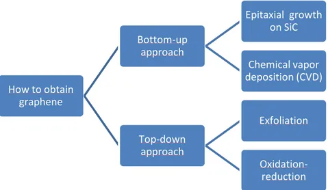
1.4 How to obtain Graphene
To produce graphene, there are two ways you could choose: bottom-up and top-down approaches.
The bottom-up approach takes the atoms and uses it to construct the desired structures, usually using the CVD technique. In the top-down approach, the graphite is used as a raw material to obtain graphene layers.
Between this two approaches there are several methods for produce graphene as can be seen in Fig.3, more information will be given below.
15
In the epitaxial growth of graphene on SiC, heating the sample results in the sublimation of Si atoms, while C atoms organize spontaneously in an honeycomb graphene layer on the surface[9].
Chemical vapor deposition (CVD) is a process where a substrate is exposed to a hydrocarbon gas (normally ethylene or methane) that decomposes onto the surface leaving adsorbed carbon atoms which, under suitable temperature conditions, can arrange in a graphene layer. Historically, graphitic layers were formed over Ni by exposure to hydrocarbons[1]. The first reported work on graphene layers produced by this method were in 2008 by Q. K. Yu and his group that used Ni[10] as a substrate and X.Li et al that used Cu[11]. This technique has, as advantages that the quality of the samples is extremely high (low defects density), has acceptable lateral dimensions( monolayers of the order of mm) and it is easy to control the thickness.
1.5 Experimental apparatus
1.5
Experimental apparatus
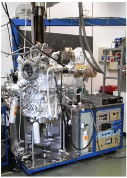
Experiments were carried out at the Surface Nanoscience Laboratory of the Department of Physics of University of Calabria (Unical) in an ultra-high vacuum (UHV) chamber made of stainless steel capable of a base pressure of 2x10⁻¹⁰ mbar.
How to obtain graphene Bottom-up approach Epitaxial growth on SiC Chemical vapor deposition (CVD) Top-down approach Exfoliation Oxidation- reduction
16
Ultra-high vacuum is the vacuum regime characterized by pressures lower than about 10−9 mbar and it is a necessary condition for many surface analytic techniques to reduce surface contamination, by reducing the number of molecules reaching the sample over a given time period. Typically, UHV requires high pumping speed, possibly multiple vacuum pumps in series and/or parallel. The sample inside the vacuum chamber can be translated, rotated and heated by a manipulator. To avoid perturbations to the electron trajectories, all the internal surfaces are grounded, and two -metal screens inside the chamber limit the intensity of the magnetic field.
The chamber is divided in two sections, which communicate through an hole in the inner -metal shield. The upper part contains a conventional electron gun that generates an electron beam with energy in the 20-2000 eV range, an X-Ray source which can generate Al and Mg Ka lines, and an hemispherical analyzer to measure energetic spectra of the electron emitted by the sample. In the upper part is also present a Retarding Field Analyzer to study the diffraction of low-energy electrons (LEED), and a gas line to fill the chamber with the desired gases. Also at this level is present an ion gun to clean the surfaces under investigation. At this level it is possible to perform Auger Electron Spectroscopy (AES), X-Ray Photoelectron Spectroscopy (XPS), Low Energy Electron Diffraction (LEED) and conventional Electron Energy Loss Spectroscopy (EELS).
The lower part of the chamber contains an High Resolution Electron Energy Loss (HREELS) spectrometer, made of a fixed monochromator and a rotating analyzer, both based on hemispherical electrostatic analyzer with mean radius of 50 mm.
17
The monochromator generates a collimated electron beam with energy in the range 0-300 eV. Scattered electrons are analyzed by the rotating analyzer, which has an acceptance angle of 2°
Ion Gun
The ion gun consists of a cathode which emits electrons by the thermionic effect, that are accelerated and spiralized to ionize Ar atoms inside the gun. Such ions are then accelerated towards the sample to remove contaminants by the sputtering effect. Such a procedure results not only in the cleaning of the surface, but also in the degradation of the surface order, which is usually recovered by annealing the sample at a suitable temperature, allowing the surface atoms to rearrange in their crystalline lattice.
Electron Gun
The system contains two different electron guns. The one present in the upper part is a conventional gun, in which electrons emitted by an heated filament are accelerated and focused to the sample, to carru out AES and EELS spectroscopies. The gun present in the lower section of the chamber, which is part of the HREELS spectrometer, generates a monochromated electron beam, employed to investigate the electronic and vibrational properties of surfaces. Also in this case, an hot filament emits electron with an energy spread which is unsuitable is we want to distinguish energy loss peaks close in energy, so we need monochromatic electron, with a spread of few meV. The monochromatization is obtained by passing electron in an hemispherical capacitor with radii R1 and R2 and through an electrostatic lens system, as shown in fig. 5.
18
Fig. 5 Hemispherical selector
Different voltages are applied to the hemispheres, so among the electrons entering at S with different energies , only those with energy Epass will follow a circular path with radius R0=(R1+R2)/2. The pass energy is related to the potential difference between the inner and the outher sphere by the relation
In this way the hemispherical capacitor is able to decrease de energy spread of the electron beam. Of course, the monochromatic beam will have a proper spread, determined by the finite apertures S and F, so the electron beam energy is Epass ± E, which can be considered as an error in the determination of Epass. The energy spread E depends on Epass, on the width d of the slits S and F, and on the angular acceptance a according to the equation
After passing through the capacitor, the electron beam is focused on the sample by two planar electrostatic deflectors and by an electrostatic cylindrical optics.
19 Electron analyzers
Due to the interaction with impinging electron or X-rays, the sample emits electrons in different directions. Such electrons have to be energy scanned to investigate the properties of the surfaces. The electron analizers in the upper and in the lower parts of the experimental apparatus consist of hemispherical capacitor similar to that shown in fig. 5. The electron coming from the sample in the solid angle determined by the aperture of the analyzer are focused by an electrostatic optics into the capacitor, and then dispersed by the capacitor depending on their energies. The electrons which follow the right path at the energy Epass are then detected at the exit. If this detection is made while scanning the potential difference E between the spheres, an energy spectrum is obtained. As mentioned above, lower values of Epass implies a lower energy indetermination, so a retarding potential at the entrance of the selector reduces the energy of the incoming electrons down to the Epass value. By changing the retarding potential it is possible to scan the energy and intensity of all the electrons, while, maintaining fixed the pass energy value, the instrumental energy indetermination remains constant for the whole spectrum. Moreover the analyzer can rotate around the z axis so it is possible to acquire energy spectra at different angles respect to the normal to the sample.
As for all experimental instruments, increasing of accuracy (low Epass) implies a decreasing in the intensity of signal and vice versa, so a good setting is a good balance between these two conditions.
1.6 Experimental techniques
1.6.1 Low-energy electron diffraction (LEED):
The Low Energy Electron Diffraction (LEED) is a technique which allow to study the surface long range order of crystalline materials by studying the diffraction of a collimated beam of low energy electrons (20-200 eV). If electrons are represented by plane waves with wavelength in accordance to the de Broglie hypothesis
20
it is clear that diffraction will take place if the electron beam energy is in the above range.
The interaction between the incident electrons and the scatters on the surface is conveniently described using the reciprocal lattice of the surface. In three dimensions, the primitive reciprocal lattice vectors are related to the real space vectors a, b and c in the following way:
, ,
For an incident electron with wave vector , the condition for constructive interference and hence for diffraction is given by the Laue condition
Where is the scattered wavevector and is a vector of the reciprocal lattice, with (h,h,l) a set of integers. The magnitude of the wavevectors k and k0 is the same, because only elastic scattering is considered. In two dimensions, the Laue condition reduces to the form
,
where and are the primitive translations vectors of the two-dimensional reciprocal lattice of the surface, and and denote the component parallel to the surface of the reflected and incident electrons respectively.
Fig. 6 Ewald’s sphere construction for the case of diffraction from a 2D-lattice. The intersection between Ewald’s sphere and reciprocal lattice rods define the allowed diffracted beams.
21
Elastically reflected electrons are revealed by a retarding field analyzer (RFA) with an integrated electron gun, as schematically shown in fig. 7.
Fig. 7 Diagram of the LEED optics
The electron gun can produce electron which are accelerated and focused into a beam, typically about 0.1 to 0.5 mm wide, by a series of electrodes serving as electron lenses beams. with the energy of 20-200 eV. Some of the electrons incident on the sample surface are backscattered elastically, and diffraction can be detected if sufficient order exists on the surface. A series of metallic grids (three or four) are used for screening out the inelastically scattered electrons; the first grid screens the space above the sample from the retarding field, the next grid is at a potential to block low energy electrons and is called the suppressor. Only the elastically scattered electrons are accelerated and hit a fluorescent screen producing on the screen the projecting of the reciprocal lattice of the sample. The screen usually is located on the wall of the vacuum chamber and it’s possible to observe the diffraction LEED pattern from the outside. By looking at fig. 6, it is clear that the image observed on the fluorescent screen is a direct picture of the surface reciprocal lattice.
22
Fig. 8 LEED used for the experiments on this thesis
1.6.2 Auger spectroscopy
Auger spectroscopy measures the kinetic energy of the emitted electrons, determines the composition of materials depending on the depth, film growth and cleanliness in the surface.
In 1920, Klein and Roseland observed the relaxation of an excited atom can be obtained through photon or electron emission and this is the physical process that forms the base of Auger spectroscopy. In 1923, P. Auger found that the energy of the emitted electrons was independent of the frequency of the primary X-ray beam and the electron energy was characteristic for each element. The first AES surface analysis was performed by Lander in 1953 using UHV.
Auger effect happens when a vacancy in an inner shell of an atom is created. After that, the vacancy is occupied by an electron from a higher energy level, and the emitted energy is transmitted to a third electron that leaves the crystal with an energy KE that mathematically can be represented as
Where
is the energy of the atom with a vacancy
23
Is the energy of the electron that leaves the crystal.
Auger Electrons are classified in the base at the energetic levels that participate in the process.
Fig. 9 Schematic representation of an Auger process
One of the advantages of this technique is the ability to analyze just a fragment of the surface, the limitation of this technique is that the samples must be solid. Because its high sensitivity was used for appreciating crystal growth and monitor during cleaning surfaces of samples, detecting impurities in the surface and interface.
Is a useful complement to LEED because Auger electron comes from about the same depth making possible the analysis of the region that determinates the diffraction pattern[12].
When AES is combined with EELS is easy to obtain information about the bulk composition and bonding.
1.6.3 X-ray Photoelectron spectroscopy(XPS)
XPS consists in irradiating a surface with monoenergetic soft X-rays and in analyzing in energy the photoelectrons emitted. Each element of the periodic table has a unique spectrum, related to the binding energies of its electronic energy levels. The spectrum from a mixture of elements is approximately the sum of the spectra of the single constituents. Because photoelectrons have small mean free paths, XPS is a surface-sensitive technique. Quantitative measurements of surface atomic concentrations can be obtained by peak heights or peak areas, and the high resolution determination of the peak positions can allow the identification of chemical states. A conventional XPS system is made of a source of X-rays, based on the emission of X-rays from a magnesium or
24
aluminum anode bombarded by electrons with energy of the order of some keV. Non-monochromatic magnesium X-rays have a wavelength of 9.89 angstroms which corresponds to a photon energy of 1253 eV. The energy width of the non-monochromatic X-ray is roughly 0.70 eV, which, in effect is the ultimate energy resolution of a system using non-monochromatic X-rays. The energy of the photoelectrons depends on the photon energy according to the following equation:
where K is the kinetic energy of the detected electron, hv is the energy of the incident photon, is the binding energy of the involved atomic orbital, and f is the analyzer work function. The binding energy is a characteristic of a specific element, in fact, usually, the XPS spectra are represented as function of the binding energy and each peak of these spectra can be used to identify the presence of the element that has a unique set of binding energies. As said above, in addition to photoelectrons emitted in the photoelectric process, Auger electrons may be emitted because of relaxation of the excited ions remaining after photoemission. The Auger peaks energy (EA) are independent from the photon incident energy, so in the binding energy representation of XPS measurements, the Auger energies are given by:
For many XPS investigations, it is important to determine the relative concentrations of the various constituents. Methods have been developed for quantifying the XPS measurement utilizing peak area and peak sensitivity factors. This approach is satisfactory for quantitative work. For a sample that is homogeneous in the analysis volume, the number of photoelectrons per second in a specific spectra peak is given by:
where n is the number of atoms of the element per cm3 of the sample, f is the x-ray flux, is the photoelectric cross section for the atomic orbital of interest, is an angular efficiency factor for
the instrumental arrangement based on the angle between the photon path and detected electron, is the efficiency in the photoelectric process for formation of photoelectrons of the normal photoelectron energy, is the mean free path of the photoelectron in the sample, A is the
area of the sample from which photoelectrons are detected and T is the detection efficiency for electrons emitted from the sample. From previous expression we obtain
25
and the denominator can be defined as the atomic sensitivity factor S. If we consider a strong line from each of two elements, then = . Therefore, a general expression for determining the atom fraction of any constituent in a sample, Cx , can be written as an extension of previous equation
Cx = =
For transition metal spectra it is best to include the entire 2p region when measuring peak area. It has to be noted that an overlying contamination layer can affect this quantitative analysis, because atoms placed only on the surface have the effect of modifying the intensity of electrons coming from underlying layers, diminishing the intensity of high binding energy peaks more than that of low binding energy peaks.
1.6.4 Electron energy loss spectroscopy (EELS)
1.6.4.1 Introduction
Electron Energy Loss Spectroscopy (EELS) is used to investigate the excitations in a crystal, caused by an incident electrons beam called primary beam, by analyzing the energy spectrum of electrons backscattered from the surface. Primary electrons can interact with electron clouds of the sample and transfer some of its kinetic energy to them. There are two kinds of EELS, they are:
1. Electron Energy Loss Spectroscopy (EELS)
2. High Resolution Electron Energy Loss Spectroscopy (HREELS)
EELS uses electrons from 0.1 to 10 keV originating from a conventional electron gun. The incident electrons beam interacts with the surface of the material of interest and the reflected beam contains inelastically scattered electrons whose energy is decreased by amounts corresponding to
26
characteristic absorption energies in the solid. Bulk and surface plasmons are the principal features of these spectra.
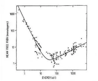
HREELS - The high resolution energy in the incident beam is achieved by monochromatizing a thermionic electron beam. The incident electrons are of quite low energy (a few eV) and the losses are in the meV range. This technique allows to study in detail the low-energy plasmons, the phonons and the vibrational properties of adsorbates. As such, it is a competitive technique with Reflection Absorption Infra Red Spectroscopy (RAIRS). RAIRS has the advantage of significantly greater energy resolution, but HREELS can study vibrational features of energy right down to a few meV (depending upon the width of the incident beam). The energy of the primary beam has fundamental importance to understand how deep the sample is probed. The figure 10 represents the mean free path (counted in monolayers) versus the energy of the incident electron beam.
Fig. 10 Electrons mean free path as function of their energies
The mean free path, that is the mean distance covered by an electron in a medium before to undergo an inelastic collision, shows a minimum around 50 eV, and after this minimum, increasing primary energy implies the increasing of the mean free path. This graph is universal, it means that it’s a good estimate of electrons mean free path in all media, and also shows that to probe more than 10 monolayers (10-20 Å) of materials it’s necessary to use electrons of more than 1000 eV of energy. Therefore, all our HREELS measurements, carried out at a primary energy of about 100 eV, carry informations mainly coming from the first atomic layers of the sample.
27
1.6.4.2 EEL spectrum
In electron energy-loss spectroscopy, we deal directly with the primary process of electron excitation, in which primary electrons undergo losses of different amounts of energy. A portion of the primary electrons scattered by the sample are analyzed by the high-resolution electron spectrometer, that separates the electrons according to their kinetic energy and produces an electron energy-loss spectrum showing the number of electrons (scattered intensity) as a function of their decrease in kinetic energy.
Many of the scattered electrons have almost the same energy of the incident electron beam (elastic peak), while some electrons are emitted with lower energy with respect to the primary energy. These latter are inelastic electrons and the energy they lost (Eloss) is the same energy that the crystal absorbed to produce an excitation.
The sample excitations induced by an electronic perturbation, are mainly divided into three groups, each for a specific energy range:
1. Core electron excitations (Eloss of the order of hundreds of eV)
2. Valence band excitations (single particle interband or intraband transitions), surface and bulk collective excitations (plasmons) (Eloss of the order of tens of eV)
3. Vibrational excitations of the sample (acoustic and optic phonon) and vibrational excitations of atoms or molecules adsorbed on the surface (Eloss of the order of meV)
28
Fig. 11 Energy distribution of the electrons emitted by the crystal after the interaction with a primary electrons beam of energy Ep
In the previous graph is plotted the general energy distribution N(E) of the electrons emitted by the crystal as a result of the interaction with a primary electrons beam of energy Ep. The graph can be divided in four sections, representing different ranges of Eloss with different sample information:
The region I includes the highest peak of the energy distribution with energy Ep that is the elastic peak and allows finding information about the structure of the sample. It contains all electrons that are reflected by the specimen with an elastic interaction only. In the vicinity of the elastic peak, there are vibrational excitations which can be determined only by the high resolution EELS (HREELS). By means of these losses it is possible to obtain information about the vibrational modes of the crystal (phonons) and the vibrational excitations of atoms and molecules adsorbed on the surface.
29
In the second region (II) it is possible to distinguish all the electrons that had inelastic interaction with the solid. The EELS spectroscopy is used, in this energy range, to have information about surface and bulk collective excitations and also about its dielectric function. Here, the plasmon peaks are the predominant features.
In the third region (III) are electrons which suffered higher energy losses, and secondary electrons at high energy. In this energy range can be found Auger electrons and core electron excitations. As in an X-ray spectrum there are additional peaks at well-defined sites in the EELS above the background. These ionization edges appear at electron energy losses that are again typical for a specific element and thus qualitative analysis of a material is possible by EELS. The onset of such ionization edges correspond to the threshold energies that are necessary to promote inner shell electrons from their energetically favored ground state to the lowest unoccupied levels. These energies are specific of the shell and of the element. Above this threshold energy, all energy losses are possible since an electron transferred to the vacuum might carry any amount of additional energy. If the atom has a well-structured density of states (DOS) around the Fermi level, not all transitions are equally likely. This gives rise to a fine structure of the area close to the edge that reflects the DOS and gives information about the bonding state. This method is called electron energy loss near edge structure (ELNES). From a careful evaluation of the fine structure farther away from the edge, until hundreds eV above the core excitations, information about coordination and interatomic distances are obtainable (extended energy loss fine structure, EXELFS).
The last region (IV) contains an high and wide peak caused by the secondary electrons, also this peak has a fine structure that can be analyzed by the angle-resolved Secondary Electron Emission (SEE). This analysis provides information about the density and the dispersion of empty states just above the Fermi level.
30
There are several basic ways to perform EELS, primarily classified by the geometry and by the kinetic energy of the incident electrons. Probably the most common today is transmission EELS, in which the kinetic energies are typically 100 to 300 keV and the incident electrons pass through the material sample. Usually this occurs in a transmission electron microscope (TEM), although some dedicated systems exist which enable extreme resolution in terms of energy and momentum transfer at the expense of spatial resolution.
The transmission EELS can be used on very thin sample, because the analyzer acquires the electron beam that passes through the material (transmitted beam) and from this analysis it’s possible to extract proprieties about the bulk of the sample. The first reports of this spectroscopy was about the transmission geometry and it was used a primary beam of (50-200 KeV) on thin samples [13]–[16]. Instead, the reflection geometry is particularly sensitive to surface properties but is limited to very small energy losses such as those associated with surface plasmons or direct interband transitions. Lucas et al [17] made the first publications about this, followed by Evans[18], [19] and Mills[20].
The EELS spectroscopy has several analogies with the optic one, in fact both techniques give information about the density of electronic states in the examined solid. EELS, however, makes it possible to change easily the energy of the incident beam, in order to probe a larger energy range. Furthermore, the low mean free path of electrons in the reflection geometry makes this technique more sensible to the surface proprieties with respect to optical spectroscopy.
31
1.6.4.3 EELS theory
In a continuous and homogeneous medium, the response to an electric external perturbation can be described by the dielectric theory. When an electron approaches a dielectric material, the electrons density inside the solid changes to shield the long range electric field produced by the incoming perturbation. The density fluctuations generated inside the medium are related to the wave vector and the frequency of the external field, so the transferred energy depends on the field density energy variation inside the solid.
An electron inside the solid can acquire energy and impulse , because of inelastic interaction with an incident electron, if it lost the same amount of energy .
The incident electron can be described by the electronic distribution:
The interaction potential produced inside the solid follows the Poisson equation:
If we pass in the Fourier space, the transform function of is:
The energy loss of the electron in length unit inside the medium is , where is the component of the electric field along the x axis, perpendicular to the surface.
Whereas
Replacing in this equation, the expression found for we obtain the loss energy probability in length unit as function of the exchanged moment and of the frequency :
32
is the bulk loss function.
So the bulk loss function describes the inelastic interaction of high energy electrons that pass through the sample.
A maximum in the loss function occurs when and . One can see the large oscillations and response will occur if , which takes place at the plasma frequency.
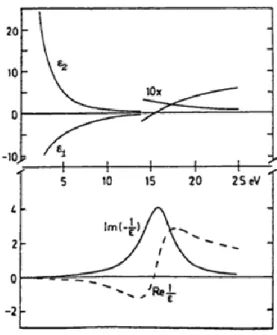
The most used models to describe a solid material are the Drude and Lorentz models. The first one deals the conduction electrons as a free electrons gas not subject to atomic potential, and in this case the dielectric function, in the limit of , is:
where is the plasma frequency and is the relaxing time that takes into account the interactions between the electrons.
33
Fig. 12 Real and imaginary part of the dielectric function (upper side) and real and imaginary part of of 1/ (bottom side) for the Drude model.
The imaginary part of the dielectric function, is monotonically decreasing and does not exhibit any structure, so a free electron gas does not generate any optical absorption. The loss function, instead, exhibits a maximum at the plasma frequency , corresponding to the excitation energy of a bulk plasmon in a free electron gas (from several eV to few tens of eV).
Lorentz model is based on treating electrons as damped harmonically bound particles subject to external electric fields. This model describes successfully bound electrons in a solid interacting with an electric field E and affected by an elastic-like restoring force with a own resonance frequency . Furthermore, to adapt, this ideal model to the experimental reality, the existence of a viscous term is assumed that can explain the linewidths experimentally observed and avoid annoying divergences. The real materials have different resonances with different intensities, so it is associated at the resonance frequency , an empirical parameter called oscillator strength factor through which it possible to weigh the different intensities, so it satisfies the relation:
To obtain the Lorentz oscillator relation, in the single resonance frequency case, we start from the second law of dynamics:
34
Where is the electron mass, is the electron charge and is the electron external field applied to the material. Solving the equation for and replacing the external field by , it is obtained:
Using the equations for the microscopic dipole and for macroscopic polarization it is extracted:
Knowing that polarization and electric field are related through the equation the dielectric function, for just one type of transition is
Where is the plasma frequency and is the oscillator strength factor.
So for different resonances the real and imaginary part of the dielectric function, respectively and , are:
Generally this is a good approximation for semiconductor, insulators and for all metals which possess bound electrons (d or p valence electrons).
35
Fig. 13 real and imaginary part of the dielectric function (upper side) and real and imaginary part of 1/ (bottom side) for the Lorentz model.
The peak in function represents an optical absorption at , while the loss function exhibits a maximum at a frequency > where and The occurrence of these conditions corresponds to a collective excitation in the solid known as “interband plasmon” in analogy to the free electron model.
More generally the behavior of metals is described by a dielectric function that is the sum of the intraband type (Drude model) and the interband type (Lorentz model). So the dielectric function is described by:
Observing trends of and for metals and semiconductors, it’s clear that the maximum of these two function are never in the same energy position, on the contrary we can assume that the maximum of matches with the minimum of , like if
.
In conclusion this is the evidence that the single particle excitations and the collective excitations are generally in competition, making the EEL probability, in the range of 1-20 eV, inversely proportional to the optical absorption.
36
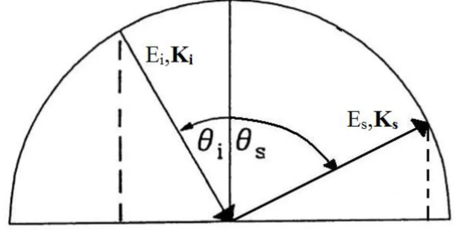
1.6.4.5 EELS in reflection geometry:
The schematic representation of the EELS in reflection geometry is shown in the following image:
Fig. 14 EELS reflection geometry representation
We assume that an electron with energy and wave vector hits the sample at an angle of incidence with respect to the surface normal and it scatters off the crystal with energy and wave vector at an angle .
We are describing an inelastic process, so the incident electron can transfer energy ( ) and momentum ( ) to the sample. From the conservation rule of energy we know that:
The conservation of the component parallel to the surface of the momentum is more restrictive, in fact just the component parallel to the surface must be preserved.
So, for the momentum we have:
Therefore, the component parallel to the surface of the momentum transfer is calculated as
Taking into account the relation between the energy and the momentum for a free electron we can calculate :
37
Thus, using monochromatic electron beam with a rotating analyzer it is possible, for each loss energy, calculate the component parallel to the surface of the momentum transfer obtaining the energy dispersion curve of the observed loss .
In the case of a 3D material, the dispersion curve shows a quadratic dependence on the momentum.
More precisely for a bulk plasmon described by the Drude model:
The bulk loss function, , found above for EELS in transmission geometry, cannot explain surface excitations treated by Mills theory[9]. For what concern electron energy loss spectroscopy in reflection geometry, we should consider the solid as a semi-infinite dielectric half-space in z≤ 0. In semi-infinite medium, Mills theory ascribes the inelastic diffusion process at the surface to electron density fluctuations induced by an incident electron on a semi-infinite materials. The loss probability function becomes proportional to:
called surface loss function.
The collective surface excitation lies at the interface between the sample and the vacuum, and the vacuum dielectric constant must be taken into account. For this reason we found “+1” at the denominator. In this case the loss probability has a pole at and . These conditions corresponds to the excitation of a surface plasmon excitation.
We can handle this process with the same theoretical concepts used for the EELS theory in transmission geometry, resulting the surface plasma frequency at:
38
It must be noted that the excitation frequency of a surface plasmon is closely connected to its counterpart in volume.
Others maxima in the loss function are in correspondence of peaks, displeased by a factor .
A surface plasmon can be understood as a crystal mode which propagates on the surface and is greatly attenuated in the direction perpendicular to it. Generally, EELS investigations in reflection geometry are a linear combination of both loss functions (bulk and surface ones) and the proportionality coefficients depends on the primary beam energy and experimental conditions.
39
1.7 Results
The Ni(111) was cleaned by repeated cycles of sputtering with 2 keV Ar ions and annealing at 1000K, until a sharp LEED pattern and the Auger spectrum showed a clean and ordered surface.
To grow graphene over Ni (111), UHV chamber worked with a base pressure of 2x10⁻¹⁰ mbar. The sample was held at a temperature of 750 K and was exposed to 1000 L (1L=10-6 mbar) of ethylene (C2H4) at 10-6 mbar partial pressure.
After the finalization of this process, Auger spectroscopy was used for its high sensitivity to the chemical composition of the sample and was observed that carbon was deposited in its graphitic form (See Fig. 16).
Fig. 16 Auger spectroscopy of graphene over Ni(111)
Low-energy electron diffraction (LEED) was used to observe the reciprocal lattice of graphene over nickel, with the result that the graphene is indistinguishable from the nickel substrate because they have similar reticular parameters, at this situation, could be said that graphene is in perfect register with nickel (fig. 17).
40
Fig. 17 LEED of graphene over Ni(111)
Various EELS spectra were taken at different angles and plasmon was observed. The spectrum in fig. 11, taken with a primary energy of 100 eV and incident and analysis angles of 45° and 39° respectively, shows the presence of the -plasmon centered at about 7 eV.. In the same figure, is also presented the spectrum obtained by subtracting from the above spectrum, that obtained in the same geometry on the clean Ni surface. In the subtracted spectrum, where de Ni contribution has been eliminated, the plasmon peak is even more evident.
41
Fig. 18 EELS spectrum of Graphene on Ni(111) (incidence 45°, analyzer 39°), the red spectrum is the above spectrum after the subtraction of Ni(111) clean spectrum.
With the values observed for Plasmons in different angles, a dispersion curve has been created and the form of the curve is a square root that represents the interband transitions of a two-dimensional plasmon.
42
Fig. 19 Graphene on Ni(111) dispersion curve [21]
After this analysis, Cs atoms were dosed onto the graphene-Ni(111) system at room temperature. Cesium is deposited over an out gassed filament that is used for sublimation. Cs coverage was controlled with Auger spectroscopy and LEED, Cs formed a ordinate structure called p(2x2) with a coverage of 0.25 ML (one monolayer is defined as the number of Cs atoms that equal those of the Ni(111) surface)[21].
After the saturation of the surface with Cs atoms, Auger spectra were collected repeatedly while increasing the temperature in rates of 50 K. In the first Auger spectra is clearly visible the cesium peak and a low contribute of carbon. When the temperature increases cesium peak decreases and the C Auger peak increases. When the carbon intensity is equal to that measured for graphene on Ni(111), the presence of a residual intensity of the Cs peak can be interpreted as due to Cs atoms located in some space between graphene and nickel.
43
In literature Eberlein et al[22], reported the values of the collective excitations for different layers of graphene obtained by Scanning transmission electron microscopy (STEM). -plasmon is observed at 4.7 eV in the single layer.
Fig. 21 Scanning transmission electron microscopy(STEM) images of Plasmon contribution of Graphene different layers[22] Fig. 20 Cs Auger calibration by using the p(2x2) Cs
44
The EELS spectra of the system Cesium-graphene-Ni(111) reveals the -Plasmon peak at 7eV [21] , Fig. 16 shows the curve, which has a quasi-linear behavior, similar to the free-standing graphene dispersion curve reported by M.K Kinyanjui et al [23].
Fig. 22 Energy loss values of the interface- p-plasmon peak plotted vs q for the Graphene/Ni(111) filled circle and for the Graphene/Cs/Ni(111) system (open circle)[21]
The results are then indicative of an almost perfect isolation of the graphene layer by the intercalated Cs atoms, even if some degree of hybridization is still present, giving the p-plasmon at an energy higher with respect to that observed on free-standing graphene (7 eV vs. 4.7 eV)
45
2. Graphene from graphite: Exfoliation and
oxidation
46
2.1 Introduction
One of the forms to preparing and obtain graphene is mixing graphite with some elements and compounds that can lead ( depending on the preparation ) to graphene with different degrees of defects and the improvement of the characteristic that can be used in several applications.
This approach for obtaining graphene, is known as a top-down approach. This approach has several routes to obtain graphene, but in a general view, this routes can be separated with the general titles of exfoliation and oxidation.
The first stages of those processes produces novel materials with features and functionalities lightly different to those of graphene, and can be used in applications where the graphene does not work at its finest, and for its low production cost are attractive to the scientific community , this materials , are named as “ graphene based materials”.
In this chapter, innovative approaches based in process of exfoliation and oxidation for graphene production are proposed and explored.
47
2.2 How to obtain graphene (second part)
As mentioned in the first chapter, there are several methods to obtain graphene. In the top-down approach, graphite is used as the starting material to obtain graphene layers, exfoliation and oxidation processes are the general methods in this approach.
2.2.1 Exfoliation
Exfoliation is the removal of the outermost layer of a solid in sheets or flakes. Exist numerous exfoliation methods, but, as a general line can be mentioned two procedures: mechanical and chemical exfoliation.
2.2.1.1 Mechanical Exfoliation:
Refers to the process where a mechanical force is used to separate graphene layers from graphite[1]. Is the most popular route to obtain graphene due to low cost and easy production. The disadvantage of this technique is that it cannot be used in many applications because the resulting material often contains agent remnants. Nevertheless, this method is still attractive as a facile method to obtain graphene due to its simplicity and the possibility of obtaining graphene with high quality[1], [24]. The more known exfoliation technique is micromechanical exfoliation for its historical value.
Early attempts to micromechanically exfoliate graphene are from 1997, when Ohashi and his group mechanically exfoliated between 20-100 layers of graphene[1].
Several groups worked in this way using AFM tip manipulation but it was in 2004, when started the boom of graphene when Geim and Novoselov exfoliated graphene using scotch-tape: they separate an characterize few and single layer graphene[25].
48
2.2.1.2 Exfoliation in the presence of solvents
The bulk graphite can be separate in layers using solution based chemistry. In this process, a polar solvent is used to break the strong Van der Waals forces that stick graphene layers and should prevent their restacking.
Many of the early successes in this kind of exfoliation came for previous works in carbon nanotubes. In 2008, Geim and Novoselov, observing the limitations of mechanically exfoliated graphene, reported a simple method in which graphite was sonicated with dimethylformamide (DMF) to produce thin graphite pieces and some monolayer sheets. Few month later, Hernandez et al[26], made the first systematic about monolayer suspensions of graphene formed with organic solvents as N-methyl-pyrrolidone (NMP)[26], N-Dimethylacetamide(DMA)[26], -butyrolactone(GBL) [26] and others.
2.2.2 Chemical preparation
The chemical preparation of graphene using a chemical treatment consists of two separated reactions: oxidation and reduction. The oxidation reaction is performed using very strong reaction parameters and media so that chemical-physics and morphological characteristics of obtained products are non-homogeneous and difficult to control. Generally, this reaction produces variously sized graphite oxide and graphene oxide materials.
On the contrary, the reduction reaction is a simple, high-yield, easy controlled reaction. For this reason, in this research work the first type of reaction has been stressed in order to realize innovations in reported preparation methods.
2.2.2.1 Preparation of Graphite Oxide by oxidation
Graphite oxide is the bulk of graphene oxide and is similar to graphite but has a larger layer spacing depending on the preparation procedure. The product has a C:O atomic ratio of 2.0 to 2.9. Is a hydrophilic material and can be easily exfoliated.
49
The chemical composition of the graphite oxide has been estimated to be approximately C4O(OH)[27].
The history of graphite oxide is the same history of graphene oxide and is really extended because started with the first studies of graphite.
Graphite oxide was prepared for the first time by B. C. Brodie in 1859 by a treatment of a mixture of potassium chlorate (KClO3) and fuming nitric acid with graphite with the resulting increase in the overall mass of the flake graphite and a molecular net formula C2.19H0.80O1.00 [28].
Approximately 40 years after, L. Staudenmaier improved Brodie’s method by adding sulfuric acid to the mix and adding the chlorate in multiples phases of the reaction[28].
Hummer’s method uses the graphite prepared with a mixture of a concentrated sulfuric acid (H2SO4), sodium nitrate (NaNO3) and potassium permanganate (KMnO4)[29] making an improvement in the quality of the oxide graphite, the preparation time (about two hours) and eliminates the formation of acid fog.
The Hummer’s method has the disadvantages of releasing toxic gases and the difficulty to remove the residual N2O4 and NO2[30].
Looking for a less aggressive treatment, Marcano et al [31] in 2010 proposed a modification of the Hummer’s method excluding NaNO3 and adding a mixture of H2SO4/H3PO4 and increasing the quantity of KMnO4.; this changes resulted in an increase in the security of the process because the production of toxic gases is reduced, and there are no large exothermic reactions. The final product is more oxidized, has more regular structure and makes less damage to the basal planes of graphite than the Hummer’s method.
2.2.2.2 Graphene oxide
GO is a hydrophilic material[32]–[36] that can form stable suspensions in aqueous media. This hydrophilic nature, combined with the high surface area and functional group density, allows for a wide variety of chemical functionalization to be performed on GO sheets. GO is considered as a building block for novel graphene based-nanomaterials[6][37].
50
GO does not exist as a static structure with a definite set of functional groups. The Ajayan model is held by the fact that GO prepared by chemical oxidation exhibits strong variance in its structure and degree of oxidation depending on the particulars oxidants used, but also on the graphite source and reactions conditions[37].
To obtain graphene oxide, graphite oxide must be exfoliated by sonication or prolonged stirring in water. Graphene oxide disperses well in water due to negative surface charges on the sheets that arises from the carboxilics acids groups and keep it from reagregating[1].
2.2.2.3 GO structure:
In graphene oxide the common functional groups are[38]:
a) Epoxy groups (C-O-C) b) Carbonil groups
c) Hydroxyl groups (OH) d) Carboxyl groups (-COOH)
The GO structure depends on the oxidation conditions, and the graphite precursor. For that reason, Dreyer et al consider that GO may be though as a family of materiasl[39] that can have differences between them. In the fig. existing models for the GO structure are proposted. There are just little modifications between them.
51
Fig. 23 Proposed atomic models for Graphene oxide[39]
Hofmann in 1939 proposed a simple models with epoxyl groups distributed randomly over the basal plane[28] Ruess suggested a structure with epoxy and hydroxyl and ether groups that forms oxygen brigdes between carbon atoms. Scholz and Boehm in 1969 presented a structure with carbonil and hydroxyl groups[28]. Nakjima-Matsuo proposted (1994), as difference from other models that oxygen atoms of epoxyl groups had adyacent layers[28].
The Lerf-Klinowsky model is the most widely accepted, this model takes elements from Sholz-Boehm’s and Ruess’, it considers that hydroxyl and epoxide groups “decorate” the basal plane which are segregated into island[39][28] and depending on the pH of the solution, the carboxyl groups are present on the edges of the sheets.
52
2.3 Zeolites
Zeolites are crystalline aluminosilicate made of elements from groups IA and IIA in the periodic table. Chemically they are presented by the general formula:
where n is the valence of cation M, is the number of water molecules per unit cell, x and y are the total number of tetrahedra per unit cell (values in the range 1-5). Zeolites consist of interconnected SiO2 and AlO2 tetrahedra and cations+ (see fig.18). Actually exist 170 different types and about 17 of them have commercial interest.
Fig. 24 SiO2 and AlO2 tetrahedra that forms zeolite.
Zeolites can be divided into natural and synthetic. Natural zeolites are minerals of volcanic origin and typically occur in cavities in basaltic and volcanic rocks. They can be found in sedimentary deposits and some occur in large monomineralic deposits suitable for mining. Zeolites can be used in adsorbent applications, concrete, paper, soil conditioner and fertilizers.[40].
The word zeolite derived from the greek words, “” and “” meaning “to boil” and “ a stone” [40].
In 1756, A. F. Cronsted discovered the first mineral zeolite. He analyzed some properties and classified them as a group inside the minerals.
21 years after, Fontana observed an adsorption phenomenon in the presence of charcoal, several groups observed in the next years that zeolite crystals could reversibly be dehydrated with
53
no apparent change in their morphology. reference In 1925, Weigel and Steinhoff reported the first molecular sieve effect[40].
The pioneering work about the zeolite synthesis and adsorption was made between mid-1930’s to 1945 by R. M. Barrer which presented the first zeolite classification[41]. depending on the dimension of the molecules and the velocity of adsorption at room temperature.
After this work, zeolites started to grow commercial interest because Barred showed a synthetic analog of a type mineral zeolite called Mordenite. [41]
Between 1949 and 1954, R.M. Milton and D. W. Breck from Union Carbide developed commercial synthetic zeolites type A, X, and Y[40].
Zeolite A was the first synthetic zeolite commercialized as an adsorbent material for separation and purification. Union Carbide started it commercialization in 1953.
Henkel in 1974 introduced zeolite A in detergents as a replacement for the environmentally suspect phosphates. Union Carbide inserts in 1977 zeolites for ion-exchange separations.
Fig. 25 Image of zeolite type A took with a Scanning electron microscope (SEM)
![Fig. 1 Unit cell of monolayer graphene, a and b are the real space unit vector. [4]](https://thumb-eu.123doks.com/thumbv2/123dokorg/2875343.9786/13.892.296.595.76.396/fig-unit-cell-monolayer-graphene-real-space-vector.webp)
![Fig. 2 Brillouin zone of monolayer graphene[4]](https://thumb-eu.123doks.com/thumbv2/123dokorg/2875343.9786/14.892.270.621.79.364/fig-brillouin-zone-of-monolayer-graphene.webp)

![Fig. 19 Graphene on Ni(111) dispersion curve [21]](https://thumb-eu.123doks.com/thumbv2/123dokorg/2875343.9786/43.892.209.681.113.530/fig-graphene-on-ni-dispersion-curve.webp)
![Fig. 22 Energy loss values of the interface- p-plasmon peak plotted vs q for the Graphene/Ni(111) filled circle and for the Graphene/Cs/Ni(111) system (open circle)[21]](https://thumb-eu.123doks.com/thumbv2/123dokorg/2875343.9786/45.892.215.591.217.700/energy-values-interface-plasmon-plotted-graphene-graphene-circle.webp)
