UNIVERSIT `
A DEGLI STUDI DI CATANIA
Dipartimento di Ingegneria Elettrica Elettronica e Informatica
Ph.D. Course in Systems Engineering (XXVI cycle) Ph.D. Thesis
MEMRISTORS AND NETWORKS:
NEW STRUCTURES FOR COMPLEXITY
Lucia Valentina Gambuzza
TUTOR: PROF. MATTIA FRASCA COORDINATOR: PROF. LUIGI FORTUNA
To my mom
“...but it was only fantasy the wall was so high, as you can see...”
Synopsis
One of the most interesting aspects of complexity is that it occurs at dif-ferent levels. It may occur at the level of interactions among the agents that compose a complex network: despite the relatively simple behavior of each single unit, the whole network may exhibit holistic collective dy-namics, such self-organization, synchronization, robustness to failure, and so on; and it may occur, in the form of an aperiodic irregular be-havior, at the level of a system described by a low-order set of ordinary differential equations, three, for instance, in the case of continuous-time systems. This thesis focuses on both levels of complexity.
The first part, in particular, deals with complexity at the level of a single dynamical system. The main contributions of the work summa-rized in this thesis refer to the use of a new electronic component for the design of chaotic circuits. This new component, the memristor, is at the same time a memory element and a nonlinear element and for this reason has been regarded in literature as an effective block to reduce the minimum number of components needed to build a chaotic circuit. The original aspect of this thesis is the focus on a realistic model of
memristor device discovered in the HP laboratories. The use of such approach introduces constraints in the design that are not considered in idealized models such as piece-wise linear ones. The main results were: i) the introduction of a configuration of two memristors in antiparallel which has been used as the fundamental block to design a gallery of autonomous and non-autonomous nonlinear circuits exhibiting a rich dynamics, including chaos; ii) the design of a hybrid circuit which takes from the characterization methodology of real memristors the idea of using a simple digital linear control circuitry which allows chaos to be observed with the driving of a single memristor.
The second part of the thesis focuses on synchronization on com-plex networks. In particular, the onset of a new form of synchronization, named remote synchronization, in complex networks has been investi-gated. Remote synchronization appears in star-like networks of coupled Stuart-Landau oscillators, where the hub node is characterized by an oscillation frequency different from that of the leaves, as a regime in which the peripheral nodes are synchronized each other but not with the hub. In this thesis we have investigated if similar conditions can be observed in more general frameworks. We have found that networks of not homogeneous nodes may display many pairs of nodes that, despite the fact that are not directly connected nor connected through chains of synchronized nodes, are phase synchronized. We have introduced measures to characterize this phenomenon and found that it is com-mon both in scale-free and Erdos-Renyi networks. Furthermore, this is
Synopsis IX an important mechanism to form clusters of synchronized nodes in a network. Finally, we have linked the appearance of pairs of remotely synchronized nodes to a topological condition of inhibition of direct paths or paths through chains of synchronized nodes, thus elucidating a mechanism which has lead to the definition of a series of topologies where remote synchronization is found.
Finally, we have explored the use of memristor as a synapse for com-plex networks. Also in this case, we have used a configuration of two HP memristors and shown that such configuration provides an adap-tation rule for the links of a complex network, enabling the emergence of a set of weights leading to synchronization.
Contents
Part I Memristors
1 The memristor . . . 1
1.1 The memristor: the theoretical postulation . . . 1
1.2 The memristor: the discovery in Hewlett-Packard labs . . 5
1.3 Memristive device models . . . 12
1.4 Memristors and flexible electronics . . . 15
2 Chaotic circuits based on HP memristor . . . 21
2.1 Introduction . . . 21
2.2 The fundamental brick: two HP memristors in antiparallel 24 2.3 The HP memristor-based Chua’s oscillator . . . 27
2.4 The HP memristor-based canonical Chua’s oscillator . . . . 33
2.5 The HP memristor-based hyperchaotic Chua’s oscillator . 36 2.6 The driven HP memristor based chaotic circuit . . . 39
3 Experimental characterization of memristors . . . 49
3.1 Introduction . . . 49
3.4 Experimental characterization . . . 59
3.4.1 Characterization of the printed memristors . . . 60
3.4.2 Characterization of the drop coated memristors . . . 61
3.5 A data driven model of T iO2 printed memristors . . . 63
3.5.1 Analysis and results . . . 64
3.6 An hybrid chaotic circuit based on memristor . . . 69
Part II Complex networks 4 Remote synchronization . . . 77
4.1 Introduction . . . 78
4.2 Remote synchronization in star-like networks . . . 80
4.3 Measures of remote synchronization in complex networks 85 4.4 Results . . . 86
5 Mechanism of remote synchronization . . . 97
5.1 Networks with a bimodal frequency distribution . . . 97
5.2 Networks with arbitrary frequency distribution . . . 107
5.2.1 Frequency-degree correlated networks . . . 108
5.2.2 FGC random networks . . . 108
5.2.3 Frequency-weighted networks . . . 110
Part III Memristors in complex networks 6 The memristor as a synapse for complex networks . . . 119
Contents XIII
6.2 Coupling a pair of nonlinear circuits with memristors . . . 121
6.3 Memristor-based synapses in a complex network of Chua’s circuits . . . 124
7 Concluding remarks . . . 127
8 Acknowledgements . . . 131
Publications . . . 133
Part I
1
The memristor
In this chapter a brief overview on memristor models will be given. The properties of the memristor, from the mathemati-cal model introduced by L. Chua, to the device realized in the HP laboratories, will be introduced and the use of the mem-ristor as nonlinear element in the design of chaotic circuits will be discussed.
1.1 The memristor: the theoretical postulation
First theoretically postulated in 1971 by Leon O. Chua [1], a memris-tor, crasis for memory-resismemris-tor, is the fourth basic circuital element. It can be defined as a dynamical resistor in which the resistance R(w) is a function of the internal state variable w or, equivalently, in which there is a relationship between charge and magnetic flux linkage. The memristor fundamental equation is a generalization of the Ohm’s law v = M (q)i, where the memristance M (q), unlike constant resistances, is function of the quantity of charge that has passed through the device.
the v − i characteristic is a straight line of slope R, in a memristor the relation is nonlinear and the v − i characteristic is a curve where the slope varies point by point. The curve takes a form of an hysteresis loop pinched in the origin, in fact whenever the voltage is zero, so is the current. In this curve the same voltage can yield to two different current values.
An important property of memristors is that the v − i characteristic depends on the frequency and the pinched hysteresis loop shrinks when the frequency increases. In the theoretical limit of infinity frequency, the memristor acts as a linear resistor.
The memristor is a nonlinear element with memory. For this reason, memristors are gaining an increasing interest in the scientific commu-nity for their possible applications, e.g. high–speed low–power proces-sors or new biological models for associative memories. Due to the intrinsic nonlinear characteristic of memristive devices, it is also possi-ble to use them in the design of new dynamical circuits apossi-ble to show complex behavior, like chaos, which is the main interest of the use of memristor in this thesis.
In its seminal paper, Leon O. Chua [1] followed arguments based on the symmetry between the four fundamental circuital variables, current i, voltage v, charge q and magnetic flux ϕ, and the corresponding three basic circuital components, resistor, capacitor and inductor. Chua pre-dicted the existence of a further basic element modeling a relationship ϕ = ϕ(q) between flux and charge (charge-controlled model) or a
rela-1.1 The memristor: the theoretical postulation 3 tionship q = q(ϕ) between charge and flux (flux-controlled model). The notable property of memristor is that, if its constitutive relationship is represented in terms of the voltage across its terminal (which is the in-tegral of the flux) and the current (i.e., the inin-tegral of the charge), one obtains a nonlinear relationship which depends on an internal variable (the charge or the flux), i.e., it acts as a nonlinear resistor (or a nonlin-ear conductance) with memory. In this way the fourth basic circuital element can be defined as a dynamical resistor in which its resistance R(w) is a function of the internal state variable w, that is a relation between charge and magnetic flux.
In terms of the v − i relationship a memristor can be conveniently defined following [1]. This passive two–terminal circuital element is described by:
v = M (q)i, or i = W (ϕ)v, (1.1)
where v, i, q, and ϕ are the voltage, the current, the charge and the flux associated to the device, M (q) is the memristance and W (ϕ) is the memductance defined as:
M (q) = dϕ(q)
dq , (1.2)
and
W (ϕ) = dq(ϕ)
of the charge–controlled and flux–controlled memristor, respectively. The concept of memristor was then generalized (again by Chua) in [2],introducing the class of memristive system defined as:
vM = R(x)iM
˙x = f (x, iM)
(1.4)
where R(x) is the memristance and f (x, iM) the internal state function
of the memristor.
The memristive device has a state variable, w, describing the phys-ical properties of the device in any time, and characterized by the two Eq. (1.4). In the first equation current and voltage are related through the memristance, and in the second equation the state variable varying as function of itself and the current flowing into the device. As results of this extension, any electronic circuit element whose resistance depends on the internal state of the system and the relation between current and voltage is a pinched hysteresis loop, could be modeled by the Eq. (1.4). The knowledge of the dependence of the state variable on the current or on the voltage is important to describe the dynamical behavior of the device. Following this generalization the memristor is a particular case of the memristive systems.
Furthermore, in [3], it was shown that the concept of memory de-vice is not related only to the resistance, but it can be generalized to capacitive and inductive systems; the authors have introduced two new classes of memory devices, the memcapacitative systems and the me-minducitve systems. The first class (charge-controlled memcapacitor)
1.2 The memristor: the discovery in Hewlett-Packard labs 5 is defined by a relationship between charge and voltage:
q(t) = C(x, vc, t)vc
˙x = f (x, vc, t)
(1.5)
where q is the charge on the capacitor, C the memcapacitance, func-tion of the internal state of the system, and vc the voltage across the
capacitor. In the plane q − vc the system shows a pinched hysteresis
loop passing through the origin. The memcapacitor changes its behav-ior depending on the frequency, in fact acts as linear capacitor at high frequency, as nonlinear capacitor at low frequency.
The meminductor systems (flux-controlled) are defined by the fol-lowing equations:
ϕ(t) = L(x, Il, t)Il
˙x = f (x, Il, t)
(1.6) where ϕ is the flux of the meminductor, L the meminductance, and Il the current flowing in the meminductor. Also in this case, when a
sinusoidal signal is applied to the terminal of the device, a pinched loop in the flux-current plane appears; increasing the frequency the memory effect decreases and the loop disappears.
1.2 The memristor: the discovery in
Hewlett-Packard labs
For many years the memristor was considered just as a mere theoretical curiosity, until the first physical realization of a two–terminal
memris-the researchers of HP labs [4]. After this first device based on a T iO2
thin film, several other memristive devices based on the same principle of the T iO2 memristor have been fabricated with different materials
and techniques (see for instance [5, 6, 7, 8, 9]). In these memristors the state depends on the oxygen vacancies that, under the effect of external bias, move from one layer to the other one, changing the resistance and the state of the device.
Memristors based on other mechanisms have been also introduced. For instance, in spin-based memristive systems [10] the memristive be-havior depends on the degree of freedom in the electron spin. In these devices the level of the electron spin polarization changes by the in-fluence of an external control parameter. As result, there is a mag-netic domain wall, i.e. a boundary between two states, that moves as a function of the external control parameter. The memristive behavior is found in a semiconductor/half-metal junction where a flow of only spin-up electrons may form, since spin-down electrons cannot enter the half-metal and form a cloud of spin-down electrons. Attention has been also devoted to develop spintronic memristors [11, 12]. In this type of device there are two ferromagnetic layers (one is the reference layer, the other one is the free layer). The free layer is divided in two parts magnetized with opposite directions creating a domain wall. The resis-tance of the device is determined by the position of the barrier between the two layers with opposite electron spin directions which in turns is controlled by the external control parameter.
1.2 The memristor: the discovery in Hewlett-Packard labs 7 The HP memristor is a T iO2 thin film, of thickness D, doped with
oxygen vacancies and sandwiched between two metal (Platinum) con-tacts as schematically represented in Fig. 1.1. The width of the doped region is indicated as w and changes as a function of the current in-jected in the device.
Fig. 1.1. Schematic representation of the T iO2 memristor.
The doped region and the undoped one have different resistivity val-ues (the doped region has a typical low value, while the undoped one an high value). When the width of the doped region is equal to the whole thickness (i.e., w = D), the memristor has a resistance equal to RON,
while, in the opposite case, when the undoped region covers the whole thickness of the device (i.e., w = 0), the memristor has a resistance equal to ROF F. In all the other intermediate cases, the HP
memris-tor is modelled as the series of two resistances, one corresponding to the region with a high concentration of dopants (of value DwRON) and
the other to the region with a low concentration of dopants (of value (1 − Dw)ROF F). In summary, the HP memristor is modelled in terms
the internal state variable w.
The width w of the doped region changes under the application of an external bias i(t) in the device: when a positive current is applied, the oxygen vacancies in the doped region move towards the undoped region, in this way the boundary between the two layer moves, causing an increase of the width of the conducting layer and decreasing the resistance of the device. When a negative current is applied, the oxygen vacancies move out from the undoped region increasing the resistance of the device. When the current is turned-off the boundary between doped and undoped region stays in its new position.
The relation between voltage and current of the HP memristor is described by the following equation:
v(t) = RON w(t) D + ROF F(1 − w(t) D ) i(t) (1.7)
The variable w(t) is limited to values between zero and D and is linked to the charge q by:
w(t) = ηµvRON
D q(t) (1.8)
or equivalently to the current i by: ˙
w(t) = ηµvRON
D i(t) (1.9)
where the parameter η characterizes the polarity of the memristor, η = 1 if the doped region in memristor is expanding, η = −1 otherwise. This is known as the linear drift model.
1.2 The memristor: the discovery in Hewlett-Packard labs 9 However, according to what experimentally observed in the HP memristor, a few volts causes a large electric field in the nano-scale device, thus producing a high nonlinearity in the ionic-drift trans-port. This nonlinearity becomes more evident at the boundaries, where w → 0 or w → D. To include this into the model, an additional term, called window function F (w), has to be inserted in the right side of the equation (1.8): w(t) = ηµvRON D F ( w(t) D )q(t) (1.10) or ˙ w(t) = ηµvRON D F ( w(t) D )i(t) (1.11)
In [4] the proposed window function depends only on the state vari-able and it is defined as:
FS(x) = x(1 − x)/D2 (1.12)
where FS(0) = 0 and FS(D) = 1−DD ≈ 0, so that it takes into account
the boundary conditions and x = w/D is the normalized state variable.. When the memristor reaches one of the boundary, x = 0 or x = D,
dw
dt = 0 and no external field can change the state. This window function
approximates the nonlinear behavior in the active layer of the device. Joglekar and Wolf [13] proposed the following window function:
FJ(x, p) = 1 − (2x − 1)2p (1.13)
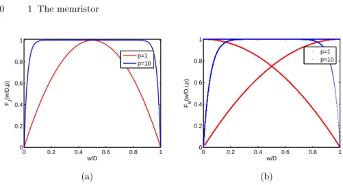
where p is a positive integer which controls the nonlinearity. The func-tion F (x) is equal to zero at the boundaries, and reaches its maximum value at x = 0.5, as it can be observed in Fig. 1.2.
0 0.2 0.4 0.6 0.8 1 0 0.2 0.4 0.6 0.8 w/D FJ (w/D,p) p=1 p=10 (a) 0 0.2 0.4 0.6 0.8 1 0 0.2 0.4 0.6 0.8 w/D FB (w/D,i,p) p=1 p=10 (b)
Fig. 1.2. Two examples of memristor window function: (a) FJ(x, p) = 1 − (2x − 1)2p for
p = 1, 5 and p = 10; (b) FB(x, p) = 1 − (x − stp(i))2p for p = 1, 5 and p = 10.
The problem at the terminal state remains and, when the state variable reaches one of the edges, its value remains unchanged for any external signal. To overcome this drawback, Biolek and colleagues [14] introduced another window function, displayed in Fig. 1.2(b), that also depends on the sign of the memristor current i:
FB(x, i, p) = 1 − (x − stp(−i))2p (1.14)
where stp(i) = 1 when i >= 0, and stp(i) = 0 when i < 0. With this window function when x = 0, the function FB(0) = 1, and when x = D,
the function FB(D) = 0. Changing the current direction, the function
immediately switches its value, FB(D) = 1 and, when x decreases to
0, the function also FB(0) = 0.
Where not differently specified, all the simulations in this thesis have been done by assuming a window function as in Eq. (1.14) with p = 1,
1.2 The memristor: the discovery in Hewlett-Packard labs 11 and the value of the technological parameters as in [4] (D = 10nm, µv = 10−14cm2s−1v−1, RROF FON = 100).
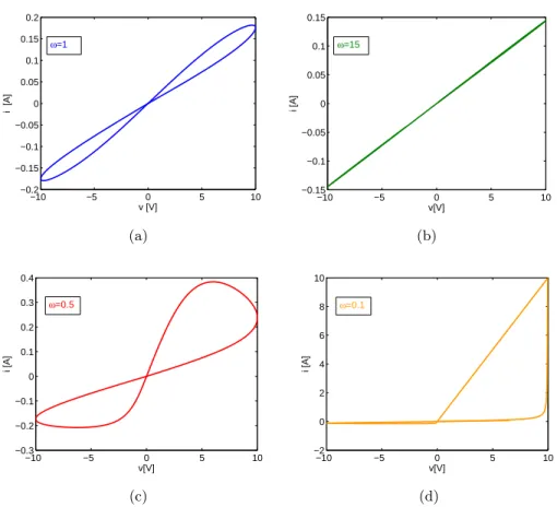
The way in which a two–terminal circuital element is shown to be memristive is to test if its v − i characteristic exhibits a pinched hys-teresis loop [1, 4]. This can be tested by applying an external bias (a sinusoidal voltage v(t)) across the device terminals and monitor-ing the current flowmonitor-ing into it (Fig. 1.3). We considered as in [14] ROF F/RON = 100 and used as in [4] normalized time units τ = t/t0
where t0 = D2/µv0 and v0 = 1V .
The behavior of the memristor depends on the frequency of the applied signal. If the frequency is comparable to the time scale of the memristor dynamics, the v −i characteristic is a symmetrical hysteresis loop pinched at the origin as shown in Fig. 1.4(a). If the frequency of the applied voltage input is larger, the pinched hysteresis shrinks into a straight line as shown in Fig. 1.4(b). However, if the frequency is smaller with respect to the time scale of the memristor dynamics, the internal state variable w may saturate to its boundary values. If such input is applied to the HP memristor, then a characteristic which is not symmetrical with respect to the applied input appears as in Fig. 1.4(c) - 1.4(d), since for w = 0 the memristor shows a resistance equal to ROF F, while for w = D the memristor shows a resistance equal to
RON. At the same time, this is the most interesting behavior for chaotic
circuit design, since it represents a highly nonlinear behavior that can be exploited to generate chaotic dynamics.
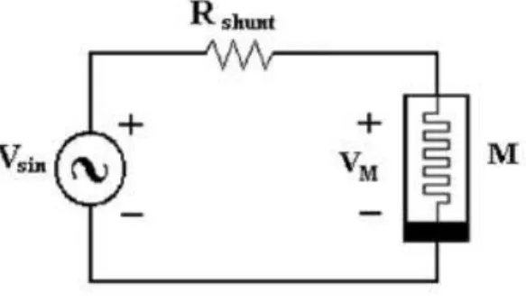
Fig. 1.3. Schematic of the circuit used to test the pinched hysteresis behavior of a single HP memristor.
1.3 Memristive device models
In the model proposed in [4] and briefly recalled in Section 1.2, the memristor properties have been attributed to the motion of oxygen vacancies activated by current flow in a T iO2 thin film device. This
model assumes that the device is constituted by two regions with dif-ferent concentrations of dopants, represented by two resistors in series. The linear drift model satisfies the characteristic of a memristive sys-tem but, even in the presence of the window function, does not fully capture the real nonlinear behavior of memristor devices.
To account for this, in [5] the authors have proposed to model the relationship between current and voltage as:
i = w(t)nβsinh(αv(t)) + χ[eγv(t)− 1] (1.15) where n is a parameter that regulates the influence of the state variable on the current, the other are fitting parameters. When w = 1 the device
1.3 Memristive device models 13 −10 −5 0 5 10 −0.2 −0.15 −0.1 −0.05 0 0.05 0.1 0.15 0.2 v [V] i [A] ω=1 (a) −10 −5 0 5 10 −0.1 −0.05 0 0.05 0.1 0.15 −0.15 v[V] i [A] ω=15 (b) −10 −5 0 5 10 −0.3 −0.2 −0.1 0 0.1 0.2 0.3 0.4 v[V] i [A] ω=0.5 (c) −10 −5 0 5 10 −2 0 2 4 6 8 10 v[V] i [A] ω=0.1 (d)
Fig. 1.4. Behavior in the v − i plane of a single HP memristor subjected to a sinusoidal input of amplitude A = 10V and frequency ω: (a) ω = 1; (b) ω = 15; (c) ω = 0.5; (d) ω = 0.1.
is in ON state and the main contribution to the current is given only by the first term in the Eq.(1.15). Otherwise in the OFF state, the current is due to the second term and w = 0.
A more detailed model has been proposed in [15] where a nonlinear and asymmetric switching behavior is adopted. A schematic view of the physical model is reported in Fig. 1.5.
Fig. 1.5. Schematic representation of the switching model proposed in [15].
The electroforming process, that is the application of an high voltage or current producing a significant change of electronic conductivity in the T iO2 structure, creates a conducting channel and a tunneling
gap between this channel and one of the electrodes. In Fig: 1.5 w is the tunneling barrier width and Rs the resistance of the electroformed
channel. The width of this gap w represents the state variable of the system, that is modulated when a voltage signal is applied to the device, inducing a motion of the oxygen vacancies. The current i that flows into the device can be modeled with Simmons tunneling equation [16]and taking into account a channel resistor, Rs, in series.
Defining as v the voltage across the whole device, vg the voltage
of the tunnel barrier, and vR the voltage across the resistance of the
channel, the relationship between the voltage v and the current i in the device is given by:
i = j0A ∆w2[ϕIe−BϕI 1/2 − (ϕI+ evg)e−B(ϕI+evg 1/2 ] vg = v − vR= v − iRS (1.16)
1.4 Memristors and flexible electronics 15 where j0 = e/(2πh), ∆w = w2 − w1, w1 = 1.2λwϕ0 , w2 = w1 + w(1 −
9.2λ
3ϕ0+4λ−2e|vg|). ϕI, B and λ are function of w, w1, w2, and ϕ0 is the
barrier height in electron volts.
The oxygen vacancy drift velocity is represented by the following nonlinear functions of i and w:
dw dt =
fof fsinh(iof fi )exp[−exp( w−aof f wc − |i| b) − w wc] i > 0
fonsinh(ioni )exp[−exp(−w−awcon − |i|
b) − w
wc] i < 0
(1.17)
where all the parameters in the equations are fitting parameters. Exper-iments on memristive devices have shown that ON and OFF switching speed are different and dependent on the polarity and on the amplitude of the applied voltage, with the OFF switching being slower. Following this model a positive voltage applied to the device produces an increase of the tunneling gap w, due to the fact that positive charged oxygen vacancies are repelled towards the conducting channel. This model pro-vides a physical explanation for the ionic transport and the switching dynamics of the T iO2 memristive devices.
This model is very accurate but of not simple use due to the expo-nential dependance of the movement of the ionized dopants and to the presence of many fitting parameters.
1.4 Memristors and flexible electronics
Recently there has been a considerable increase in the interest towards the study of chaotic circuits, thanks to the growing number of possible
provement of already existing technologies which can benefit from the peculiarities of chaos and results in improved performance.
Most of the phenomena occurring in nature, but also some human behaviors, do not proceed with rhythms that are repeated, but suddenly show bifurcations, critical points turbulence and emergent behaviors. This is a phenomenon that gives rise to so-called strange attractors. In nature there are few linear phenomena, while almost all the existing systems are nonlinear. There are some common natural phenomena such as the variation of weather and the formation of clouds that are chaotic, the heartbeat is also chaotic, an healthy heart has a chaotic rhythm, whereas in a diseased heart the rhythm is more regular. These phenomena which are the subject of of chaos theory, belong to complex nonlinear dynamical systems and share some peculiar characteristics: • sensitivity to initial conditions;
• unpredictability;
• evolution of the system characterized by many orbits that remain confined within a finite space, called attractor.
One of the most interesting aspects of the study of the dynamics of nonlinear systems is the organization that emerges spontaneously from the interaction of many elementary components. Complex sys-tems respond to the changes of the external environment, reorganizing themselves to exhibit novel properties. Self-organization is not imposed
1.4 Memristors and flexible electronics 17 from the external but naturally emerges from the evolution of the sys-tem as a function of its dynamics.
Many physical systems exhibit chaotic behavior. One of the most important is the Lorenz system obtained by discretization of Navier-Stokes fluid dynamics equations [17]. Chaos appear also in electronic chaotic circuits, either as an undesired behavior or as the result of an intentional design. The first circuit exhibiting chaos was the Chua’s circuit built in 1983. The implementations of integrated chaotic circuits are in a limited number, despite the significant benefits arising from the availability of integrated chaotic circuits. Until a few years ago the production of integrated circuits was based only on silicon devices. The processes used to create these ICs are not cheap. To address these issues, the tendency was to miniaturize the devices even more, so that they can integrate a larger number of transistors on a single wafer.
For about a decade, an alternative and efficient answer to the re-quest a low-cost technology has been searched for. In this context the use of organic materials for the manufacturing of electronic devices has been recently proposed. The devices using organic semiconductors as the active element are no longer an inorganic semiconductor like silicon or gallium arsenide, but a series of molecular materials such as conjugated polymers or small molecules. The organic electronics is economically advantageous because the active substances, based on or-ganic compounds of carbon, have important properties, including those to be flexible and easy to deposit over large areas. This can be done
processes.
Methods typical of the printing industry, such as screen printing or ink jet printing for the manufacture of electronic components can be therefore used for the realization of these devices. The ability to create devices through simple and low cost realization processes is one of the unique aspects of organic electronics. Another important advantage is the possibility to produce large-area devices with consequent reduction of production costs and reducing time. Despite the significant benefits of organic electronics, the science in this field still faces problems such as low mobility of charge carriers, which in turn requires a too high operating voltage, and the strong interaction of these materials with the environment (moisture, oxygen, light) which alters the basic properties. In the context of organic electronics, it is interesting to explore the possibility to design circuits able to generate chaos. Organic chaotic circuits in fact could be applied to the production of food packaging, which will have the opportunity to include in the package, instead of labels with a bar code or in addition to the standard bar code tag, active labels that can monitor the status of the product by controlling volatile organic compounds (odors) present in the box, typical of a certain food. If over time the product were modified (so for example if the smell would change because of the deterioration of the product), the circuit would respond immediately by signaling the event [18]. The organic chaotic circuits, thanks to the characteristics of chaos, in such labels could provide a secure key to prevent product counterfeits.
1.4 Memristors and flexible electronics 19 Organic chaotic circuit can be used in the product identification step for product traceability. The instruments most used in practice are al-phanumerical labels, bar codes and radiofrequency identification tags (RFID). Actually, products are mostly identified through bar codes which also allow to reconstruct the history of the product and its lo-calization in order to trace the product itself.
The idea is to integrate the techniques based on traditional tools for product identification with organic circuits that show chaotic dynamics when activated by an external generator. Such circuits have intrinsic safe identificability properties, since only a copy of this circuit is able to identify it. Therefore, the information encoded in this chaotic tag can be decoded only in the presence of a circuit which can be synchro-nized to it. In this way, a chaotic key to make safe the identification procedure can be added. In particular, several possibilities arise for the development of chaotic circuits in organic technology and some of them are currently being explored.
As memristors in organic, or more generally in flexible, electronics have been already fabricated, the basic idea of this thesis is to exploit the nonlinearity plus memory capabilities of such devices for designing chaotic circuits in organic/flexible electronics. For this reason in the next two Chapters we will focus on electronic oscillators where the source of nonlinearity is provided by memristors.
2
Chaotic circuits based on HP memristor
In this Chapter the design of chaotic circuits based on mem-ristors modelled with the nonlinear drift model is dealt with. This physical model, being representative of real devices, in-troduces constraints in the design that reduce the gap to the final implementation of the circuit. We propose a configura-tion based on two memristors in antiparallel as the nonlinear element for chaotic oscillators and discuss a series of nonlin-ear, autonomous and non-autonomous, circuits derived from existing topologies of chaotic circuits by replacing the nonlin-earity with such configuration.
2.1 Introduction
The availability of memristive devices, being nonlinear elements, is use-ful to design circuits able to show complex dynamics like chaos. In particular, if we consider the Chua’s circuit, the first example of elec-tronic circuit able to show chaos [19], the memristor can be used as
implemented by the Chua’s diode.
The same consideration hold for the canonical Chua’s oscillator: in particular in [20], the Chua’s diode in the canonical Chua’s oscilla-tor is replaced assuming for the memrisoscilla-tor a piecewise-linear (PWL) function: ϕ(q) = bq + 1 2(a − b)(|q + 1| − |q − 1|), (2.1) or q(ϕ) = dϕ + 1 2(c − d)(|ϕ + 1| − |ϕ − 1|). (2.2) If at least one of the two slopes of the constitutive relations, a and b for the charge–controlled memristor (or c and d for the flux–controlled memristor), is negative then the memristor is active. Otherwise, the memristor is passive. In this case, a negative resistance in parallel with the memristor is needed to guarantee that at least one active device is in the circuit, that is a well-known necessary condition for the onset of chaotic dynamics.
There are other examples of memristor-based chaotic circuits that assume an ideal characteristic for the memristor, in [21] it is shown that a chaotic circuit can be obtained with only three elements: a capacitor, an inductor and an active memristive system, whose memristance is defined as R(x) = β(x2 − 1), while in [22] a memristor with a cubic q − ϕ characteristic is considered.
2.1 Introduction 23 Concerning circuital implementations of memristor-based oscilla-tors, several approaches based on the use of discrete-component circuits mimicking ideal memristor features have been introduced. To this aim, mutators [1], multipliers [22], micro-controllers [23] or Cellular Nonlin-ear Networks [24] have been used.
Most of the memristor-based oscillators, assume ideal characteris-tics of the memristor such as, for instance, cubic or PWL nonlinearities. Here, we introduce a different approach. We start from the model of the HP memristor ([4]) and not considered in the papers mentioned above, and introduce a gallery of chaotic circuits exploiting this device model. The HP memristor is a passive non-symmetrical element having a nonlinearity different from that more frequently investigated (often symmetrical), so that its use for chaotic circuit design is not trivial. We show that using two HP memristors in antiparallel a symmetri-cal nonlinearity can be recovered and suitably adapted to become the nonlinear element of canonical topologies for chaos generation. We dis-cuss such topologies and show the chaotic attractors obtained and the bifurcation scenarios with respect to some constitutive parameters of the memristor. The analysis of the i − v characteristics of the two HP memristors in antiparallel is carried out by using the so-called Biolek’s window function.
antiparallel
We have already shown that, when the period of the input signal, ap-plied to the memristor, is large with respect to the time scale of the memristor dynamics, the internal state variable w may saturate to its boundary values. If such input is applied to the HP memristor, then a characteristic which is not symmetrical with respect to the applied input appears, since for w = 0 the memristor shows a resistance equal to ROF F, while for w = D the memristor shows a resistance equal to
RON. At the same time, this is the regime to which we are interested
to, since it represents a highly nonlinear behavior that can be exploited to generate chaotic dynamics.
We now show that a symmetrical characteristic can be recovered by connecting two memristors in antiparallel, i.e., with the two terminals shortened but with opposite polarities (Fig. 2.1). In such configuration the voltage across each memristor is equal to the voltage of the resulting two-terminal device, v = vM 1 = vM 2, while the current is the sum of the
current through each memristor i = iM 1+ iM 2. Fig. 2.2 illustrates the
behavior of this configuration (we assume as in [14] ROF F/RON = 100
and use as in [4] normalized time units τ = t/t0 where t0 = D2/µv0 and
v0 = 1V ). A sinusoidal voltage input is applied to the HP memristor
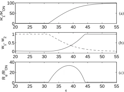
model. The amplitude A = 10V and the frequency ω = 0.1rad/s are such that the state variable w oscillates between its boundary values. Fig. 2.2(a) shows the resistance of memristor 1, clearly exhibiting a
2.2 The fundamental brick: two HP memristors in antiparallel 25 non-symmetrical behavior. Fig. 2.2(b) shows the trend of the state variables w1 and w2 associated to the two memristors (they oscillate at
opposite phases). A symmetrical behavior is obtained in the equivalent resistance (Re = 1 R1(w1)+ 1 R2(w2) −1
), as shown in Fig. 2.2(c). The same behavior can be observed in terms of pinched hysteresis. The hysteresis curve of each of the two memristors is not symmetrical, but when they are considered together the symmetry is recovered.
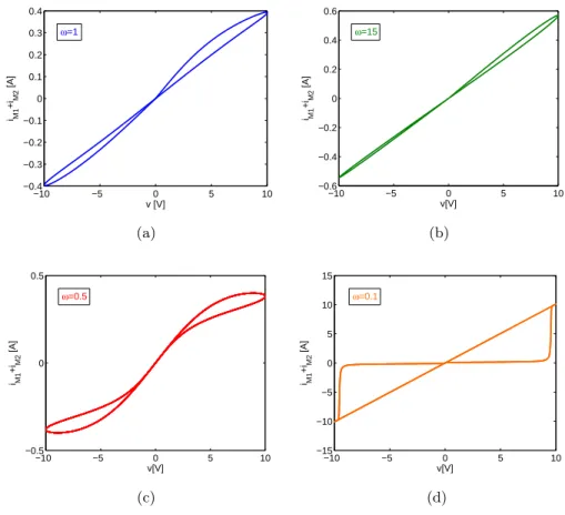
Fig. 2.3 shows the pinched hysteresis at different values of ω. Fig. 2.3(a) represents the case when the input period is comparable to the time scale of the memristor dynamics. If the frequency of the applied voltage input increases, also in this case, the pinched hystere-sis shrinks into a straight line as shown in Fig. 2.3(b). Figs. 2.3(c) and 2.3(d) represent the case when the input period is larger with re-spect to the time scale of the memristor dynamics. In particular, when ω = 0.1 an highly nonlinear behavior is obtained, since the internal state variable w saturates to its boundary values (zero and D). This is clearly the most interesting case for the design of chaotic circuits. It is worth noticing that in this latter case, even if the pinched hysteresis of each memristor is not symmetrical, as shown in Fig. 1.4(d), when the two HP memristors are considered together the symmetry is recovered. This configuration will be used to design a series of nonlinear circuits able to generate chaos starting from Chua’s oscillators and replacing the Chua’s diode with two HP memristors in antiparallel. For this rea-son it will be considered as the fundamental brick for the design of chaotic circuits based on HP memristors.
Fig. 2.1. Two memristors connected in antiparallel. 20 25 30 35 40 45 50 55 0 50 100 R 1 /R O N 20 25 30 35 40 45 50 55 0 20 40 τ R e /R O N 20 25 30 35 40 45 50 55 0 0.5 1 w 1 , w 2 (a) (b) (c)
Fig. 2.2. Behavior of two memristors in antiparallel when a sinusoidal input v(τ ) = 10sin(0.1τ ) is applied: (a) trend of R1/RON; (b) trend of w1 (dashed line) and w2
2.3 The HP memristor-based Chua’s oscillator 27 −10 −5 0 5 10 −0.4 −0.3 −0.2 −0.1 0 0.1 0.2 0.3 0.4 v [V] iM1 +iM 2 [A] ω=1 (a) −10 −5 0 5 10 −0.4 −0.2 0 0.2 0.4 0.6 −0.6 v[V] iM1 +iM 2 [A] ω=15 (b) −10 −5 0 5 10 −0.5 0 0.5 v[V] iM1 +iM 2 [A] ω=0.5 (c) −10 −5 0 5 10 −15 −10 −5 0 5 10 15 v[V] iM1 +iM 2 [A] ω=0.1 (d)
Fig. 2.3. Behavior in the v−i plane of a configuration of two HP memristors in antiparallel subjected to a sinusoidal input of amplitude A = 10V and frequency ω: (a) ω = 1; (b) ω = 15; (c) ω = 0.5; (d) ω = 0.1.
2.3 The HP memristor-based Chua’s oscillator
In this section the chaotic oscillator, obtained starting from the Chua’s oscillator by replacing the Chua’s diode with the parallel between a negative conductance and the two HP memristors connected in the configuration introduced in section 2.2, is described. The circuit, shown in Fig 2.4, consists of eight elements, namely one inductor, two
capaci-Fig. 2.4. HP memristor-based Chua’s oscillator.
tors, two resistors, a negative conductance and the two HP memristors in antiparallel.
The circuit dynamics is described by the following set of differential equations: dvC1 dt = 1 C1( vC2−vC1 R + GvC1 − vC1 R1(w1) − vC1 R2(w2)) dvC2 dt = 1 C2( vC1−vC2 R − iL) diL dt = 1 L(vC2 − riL) dw1 dt = η1µRON D F ( w1 D) vC1 R1(w1) dw2 dt = η2µRON D F ( w2 D) vC1 R2(w2) (2.3) where Ri(wi) = RON wi D + ROF F(1 − wi D) (2.4) and η1 = −η2 = 1.
We now consider the following scaling:
X = vC1/v0, Y = vC2/v0, Z = iL/i0,
W1 = w1/D, W2 = w2/D, τ = t/t0
2.3 The HP memristor-based Chua’s oscillator 29 with v0 = 1V, i0 = v0/RON, t0 = D2/µv0 C0 = D 2 µv0RON, L0 = D2R ON µv0 (2.6)
so that Eqs. (2.3) become:
dX dτ = C0 C1( RON R Y − RON R X + GRONX − X ˆ R1(W1)− X ˆ R2(W2)) dY dτ = C0 C2( RON R X − RON R Y − Z) dZ dτ = L0 L(X − r RONZ) dW1 dτ = η1F (W1) X ˆ R1(W1) dW2 dτ = η2F (W2) X ˆ R2(W2) (2.7) where ˆRi(Wi) = Wi+RROF FON (1 − Wi).
We have taken into account the following typical values for the HP memristor parameters: RON = 100Ω, ROF F/RON = 100, D = 10nm
and µ = 10−14cm2s−1v−1. This leads to i
0 = 10mA and t0 = 10ms.
For such parameters, if we set C1
C0 = 0.2564, C2 C0 = 0.75, L L0 = 0.2, GRON = 0.6, RR ON = 2.7 and r
RON = 0.01, the circuit exhibits the
chaotic attractor shown in Fig. 2.5.
As it can be noticed in the rescaled Eqs. (2.7), the technological parameters of the memristor (such as RON or µ) only affect the
nor-malization of the circuit components, with the unique exception of the technological parameter β, defined as β = ROF F/RON. Hence, the
dy-namical behavior of the HP memristor-based Chua’s oscillator is now studied with respect to this parameter. The bifurcation diagram with respect to β and the corresponding Lyapunov spectrum are reported in
−40 −20 0 20 40 −10 0 10 −20 −10 0 10 20 X Y Z (a) −10 −5 0 5 10 −20 0 200 0.5 1 1.5 Y Z W 1 (b)
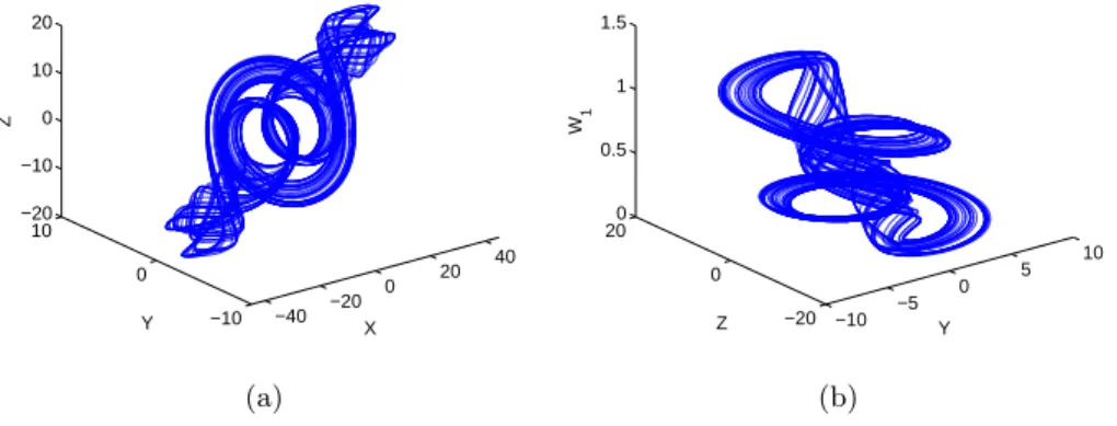
Fig. 2.5. Chaotic attractor of the HP memristor-based Chua’s oscillator: (a) X − Y − Z, and (b) Y − Z − W1phase space.
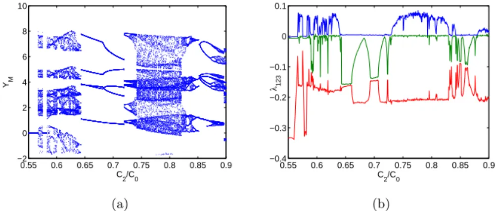
Fig. 2.6. The bifurcation diagram has been obtained by plotting the lo-cal maxima of the state variable Y . It can be observed that the chaotic behavior of the circuit is preserved for a wide range of values of β.
80 100 120 140 160 180 200 0 5 10 15 β YM (a) 80 100 120 140 160 180 200 −0.25 −0.2 −0.15 −0.1 −0.05 0 0.05 0.1 β λ1,2,3 (b)
Fig. 2.6. (a) Bifurcation diagram and (b) Lyapunov spectrum of the HP memristor-based Chua’s oscillator with respect to β. For sake of clarity the first three Lyapunov exponents λ1 (in blue), λ2 (in green) and λ3(in red) are only reported.
2.3 The HP memristor-based Chua’s oscillator 31 The circuit exhibits a rich dynamical repertoire also when the other circuital parameters (C1, C2, L or G) are changed. As an example of
the different dynamical behaviors generated by the circuit, we restrict our analysis to changes in the parameter C2
C0. The bifurcation diagram
and the corresponding Lyapunov spectrum with respect to this param-eter are shown in Fig. 2.7. Windows of chaotic behaviors and periodic behaviors appear in the bifurcation diagram as it is also evident from the analysis of the Lyapunov spectrum.
0.55 0.6 0.65 0.7 0.75 0.8 0.85 0.9 −2 0 2 4 6 8 10 C 2/C0 YM (a) 0.55 0.6 0.65 0.7 0.75 0.8 0.85 0.9 −0.4 −0.3 −0.2 −0.1 0 0.1 C 2/C0 λ12 3 (b)
Fig. 2.7. (a) Bifurcation diagram and (b) Lyapunov spectrum of the HP memristor-based Chua’s oscillator with respect to C2
C0. For sake of clarity, the first three Lyapunov exponents
λ1 (in blue), λ2 (in green) and λ3 (in red) are only reported.
Following the approach described in [25], a realization of the HP memristor-based Chua’s oscillator without inductor is obtained by ex-ploiting the well-known Wien bridge configuration. The circuit, re-ported in Fig. 2.8, consists of a resistor, a capacitor, a Wien bridge circuit, and the nonlinear active element realized through a negative
Fig. 2.8. A realization of the HP memristor-based Chua’s oscillator based on Wien bridge configuration.
conductance in parallel to the two HP memristors. Applying the Kirch-hoff’s laws to the circuit, we obtain the following set of differential equations: dvC1 dt = 1 C1( vC2−vC1 R + GvC1 − vC1 R1(w1) − vC1 R2(w2)) dvC2 dt = 1 C2(− vC3 R1 + ( R3 R4R1 − 1 R2)vC2− vC2−vC1 R ) dvC3 dt = 1 C3(− vC3 R1 + R3 R4R1vC2) dw1 dt = η1µRON D F ( w1 D) vC1 R1(w1) dw2 dt = η2µRON D F ( w2 D) vC1 R2(w2) (2.8)
By applying the same scaling reported in Eqs.(2.5), Eqs. (2.8) can be scaled as follows: dX dτ = C0 C3( RON R Y − RON R X + GRONX − X ˆ R1(W1)− X ˆ R2(W2)) dY dτ = C0 C2(− RON R1 Z + ( RONR3 R4R1 − RON R2 )Y − RON R Y + RON R X) dZ dτ = C0 C1(− RON R1 Z + RONR3 R4R1 Y ) dW1 dτ = η1F (W1) X ˆ R1(W1) dW2 dτ = η2F (W2) X ˆ R2(W2) (2.9)
2.4 The HP memristor-based canonical Chua’s oscillator 33
Fig. 2.9. HP memristor-based canonical Chua’s oscillator.
where we have assumed that the parameters have the same value of the circuit in Fig. 2.4. The behavior of this circuit is perfectly analogous to the HP memristor-based Chua’s oscillator, but the circuit avoids the use of inductors.
2.4 The HP memristor-based canonical Chua’s
oscillator
The second nonlinear circuit presented in this thesis is derived from the canonical Chua’s oscillator by replacing the nonlinear resistor with a negative conductance in parallel to the two HP memristors. The circuit is shown in Fig. 2.9 and is governed by the following equations:
diL dt = 1 L(vC2 − vC1) dvC2 dt = 1 C2(GvC2 − iL) dw1 dt = η1µRON D F ( w1 D) vC1 R1(w1) dw2 dt = η2µRON D F ( w2 D) vC1 R2(w2) (2.10)
By applying the scaling as in Eqs. (2.5), the following dimensionless equations are obtained:
dX dτ = C0 C1(Y − X ˆ R1(W1) − X ˆ R2(W2)) dY dτ = L0 L(Z − X) dZ dτ = C0 C2(−Y + GRONZ) dW1 dτ = η1F (W1) X ˆ R1(W1) dW2 dτ = η2F (W2) X ˆ R2(W2) (2.11)
Also in this case, we have observed that the circuit is able to gener-ate chaotic behavior for a wide range of the parameters. For instance, if here the parameters of the HP memristor are chosen as in the previous section and C1 C0 = 0.25, C2 C0 = 1/3, L L0 = 1.6, GRON = 0.14, the chaotic
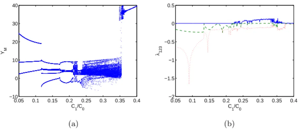
attractor shown in Fig. 2.10 is obtained. The behavior of the circuit with respect to the technological parameter β is illustrated in Fig. 2.11. Both the bifurcation diagram and the corresponding Lyapunov spec-trum clearly indicate that the onset of chaos can be observed even in presence of large variations of β from the value assumed in our simu-lations.
Fig. 2.12 reports an example of the behavior of the circuit with re-spect to one of the other circuit elements. In particular, the parameter
2.4 The HP memristor-based canonical Chua’s oscillator 35 −20 −10 0 10 20 −10 0 10 −20 −10 0 10 20 X Y Z (a) −10 −5 0 5 10 −20 0 20 0 0.5 1 Y Z W 1 (b)
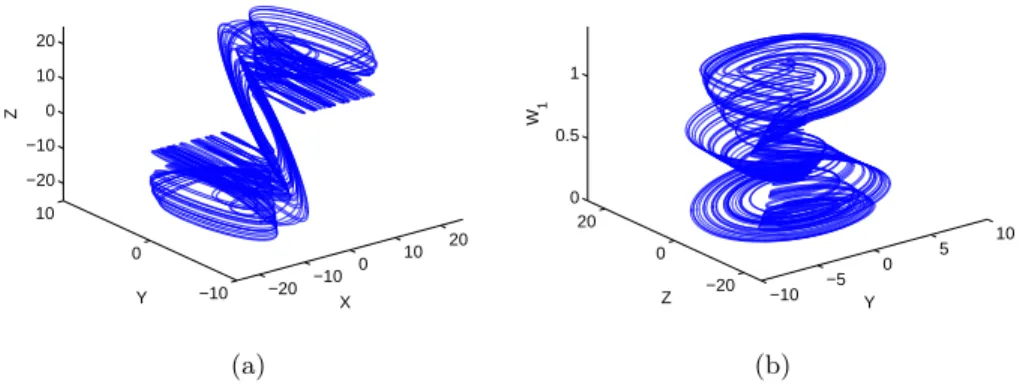
Fig. 2.10. Chaotic attractor of the HP memristor-based canonical Chua’s oscillator: (a) X − Y − Z, and (b) Y − Z − W1phase space.
0 100 200 300 400 −40 −20 0 20 40 60 β YM (a) 50 100 150 200 250 300 350 400 10 −0.4 −0.3 −0.2 −0.1 0 0.1 β λ1,2,3 (b)
Fig. 2.11. (a) Bifurcation diagram and (b) Lyapunov spectrum of the HP memristor-based canonical Chua’s oscillator with respect to β. The first three Lyapunov exponents λ1 (in blue), λ2 (in green) and λ3 (in red) are reported.
C1
C0 has been varied. The analysis of the bifurcation diagram, in
accor-dance with the corresponding Lyapunov spectrum, allows to assess the presence of several windows of chaotic behavior and of limit cycles of different periodicity.
behavior in several regions of the parameter space, which is not evident in the bifurcation diagram of Fig. 2.12, obtained for a fixed set of initial conditions. To illustrate this, we have calculated the trajectory of the system for different initial conditions. In particular, we restricted our analysis to the hyperplane with Z(0) = 0.2, W1(0) = 0.1 and
W2(0) = 0.9, while we varied X(0) and Y (0). The result of this analysis
is summarized in the map shown in Fig. 2.13, where each point of the color-coded map represents the number of different local maxima found for the state variable Y calculated at the corresponding pair of initial condition X(0) and Y (0). Four distinct attractors coexist for this set of parameters: the large green area indicates the chaotic attractor reported in Fig. 2.10, while the areas in the different blue tones indicate two limit cycle attractors (one of period-2 and one of period-3) and a stable equilibrium point 0 0 0 0.09 0.97
.
2.5 The HP memristor-based hyperchaotic Chua’s
oscillator
The third example of HP memristor-based oscillators is derived by in-troducing an additional inductor, indicated as L2, in the HP
memristor-based canonical Chua’s oscillator discussed in Section 2.4. L2 is
intro-duced in parallel to the negative conductance G, so that the circuit shown in Fig. 2.14 is obtained.
2.5 The HP memristor-based hyperchaotic Chua’s oscillator 37 0.05 0.1 0.15 0.2 0.25 0.3 0.35 0.4 −10 0 10 20 30 40 C 1/C0 YM (a) 0.05 0.1 0.15 0.2 0.25 0.3 0.35 0.4 −2 −1.5 −1 −0.5 0 0.5 C1/C0 λ12 3 (b)
Fig. 2.12. (a) Bifurcation diagram and (b) Lyapunov spectrum of the HP memristor-based canonical Chua’s oscillator with respect to C1
C0. For sake of clarity the first three
Lyapunov exponents λ1 (in blue), λ2 (in green) and λ3 (in red) are only reported.
X(0) Y(0) −50 0 50 −80 −60 −40 −20 0 20 40 60 80 0 10 20 30 40 50 60
Fig. 2.13. Color-coded map of the HP memristor-based canonical Chua’s circuit with respect to different initial conditions X(0) and Y (0) (with Z(0) = 0.2, W1(0) = 0.1 and
Fig. 2.14. HP memristor-based hyperchaotic Chua’s oscillator. dvC1 dt = 1 C1(iL1 − vC1 R1(w1) − vC1 R2(w2)) dvC2 dt = 1 C2(GvC2 − iL1 − iL2) diL1 dt = 1 L1(−vC1 + vC2 − RiL1) diL2 dt = 1 L2vC2 dw1 dt = η1µRON D F ( w1 D) vC1 R1(w1) dw2 dt = η2µRON D F ( w2 D) vC1 R2(w2) (2.12)
Eqs. (2.12) can be scaled according to the scaling reported in Eqs.(2.5), with the additional dimensionless variable Ω = iL2/i0, as
follows: dX dτ = C0 C1(Z − X ˆ R1(W1) − X ˆ R2(W2)) dY dτ = C0 C2(GRONY − Z − Ω) dZ dτ = L0 L1(−X + Y − R RONZ) dΩ dτ = L0 L2Y dW1 dτ = η1F (W1) X ˆ R1(W1) dW2 dτ = η2F (W2) X ˆ R2(W2) (2.13)
2.6 The driven HP memristor based chaotic circuit 39 We notice that system (2.12) is able to show a transition from torus to chaos and, then, to hyperchaos when the bifurcation parameter is L2
L0.
In fact, for the parameter values reported in Fig. 2.15, different attrac-tors can be observed for increasing values of L2
L0: a torus (Figs. 2.15(a)
and 2.15(b)); a chaotic attractor (Fig. 2.15(c)) and an hyperchaotic attractor (2.15(d)). The complete scenario with respect to changes in the parameter L2
L0 is illustrated in Fig. 2.16, which allows to detect the
transition from torus to chaos occurring approximately at L2
L0 ≃ 1.9 and
that from chaos to hyperchaos at L2
L0 ≃ 3.2.
The analysis of the behavior of the system when the technological parameter β is varied has been carried out by considering the circuit in the hyperchaotic region (i.e. L2
L0 = 3.6). The bifurcation diagram and
the Lyapunov spectrum shown in Fig. 2.17 allow to conclude that the hyperchaos can be obtained in the interval β ∈ [88 ÷ 194], whereas outside this interval either chaos or periodic behavior appears.
2.6 The driven HP memristor based chaotic circuit
The circuit proposed by Murali, Lakshmanan and Chua [26], in the fol-lowing referred to as the MLC circuit, is a dissipative non-autonomous circuit, made by an inductor, a capacitor, a resistor and a Chua’s diode. In this circuit the nonlinearity is modeled with a three-segment charac-teristic. The circuit is driven by an external sinusoidal signal of ampli-tude A and frequency ω. By varying the ampliampli-tude of the forcing signal, the circuit exhibits a variety of dynamical behaviors, from limit cycle
−200 −100 0 100 200 −50 0 50 −40 −20 0 20 40 Y Z Ω (a) −20 −10 0 10 20 −10 0 10 −10 −5 0 5 10 Y Z Ω (b) −20 0 20 −10 0 10 −10 −5 0 5 10 Y Z Ω (c) −50 0 50 −20 0 20 −20 −10 0 10 20 Y Z Ω (d)
Fig. 2.15. Attractors of the HP memristor-based hyperchaotic Chua’s oscillator in the Y − Z − Ω phase space. Parameter values are C1
C0 = 0.25, C2 C0 = 1/3, L1 L0 = 1.6, GRON = 0.192, and (a) L2 L0 = 1.3 (torus), (b) L2 L0 = 2.8 (torus), (c) L2 L0 = 3.2 (chaos), and (d) L2 L0 = 3.6 (hyperchaos).
to chaotic attractors. A memristive MLC circuit built by substituting the Chua’s diode with a PWL flux controlled memristor has been pro-posed in [27] and, recently, this system has been modeled as a piecewise smooth system of second order with two discontinuous boundaries and deeply numerically studied by Ishaq Ahamed and Lakshmanan [28], who have shown that it exhibits a wide range of chaotic behaviors
in-2.6 The driven HP memristor based chaotic circuit 41 1 1.5 2 2.5 3 3.5 −20 0 20 40 60 80 100 120 140 L 2/L0 YM (a) 1 1.5 2 2.5 3 3.5 4 −0.25 −0.2 −0.15 −0.1 −0.05 0 0.05 0.1 L 2/L0 λ12 3 (b)
Fig. 2.16. (a) Bifurcation diagram and (b) Lyapunov spectrum with respect to L2 L0. For
sake of clarity the first three Lyapunov exponents λ1 (in blue), λ2 (in green) and λ3 (in
red) are only reported.
50 100 150 200 −50 0 50 100 150 β YM (a) 50 100 150 200 −0.3 −0.2 −0.1 0 0.1 0.2 β λ1,2,3,4 (b)
Fig. 2.17. (a) Bifurcation diagram and (b) Lyapunov spectrum of the HP memristor-based hyperchaotic canonical Chua’s oscillator with respect to β. For sake of clarity the first four Lyapunov exponents λ1(in blue), λ2(in green), λ3 (in red) and λ4(in cyan) are
want to realize a non-autonomous chaotic circuit using a different model for the memristor, that is, a model adopted to mimic the behavior of the real memristor realized in the HP laboratories.
Starting from the MLC topology, we show how a new driven mem-ristive chaotic circuit can be obtained by replacing the Chua’s diode with our fundamental brick in parallel with a negative resistor. The proposed chaotic circuit is shown in Fig. 2.18.
Fig. 2.18. The non-autonomous memristive chaotic circuit.
The circuit dynamics is described by the following set of differential equations: dvC dt = 1 C(iL− vC R1(w1) − vC R2(w2) + GvC) diL dt = 1 L(−riL− vC+ A sin ωt) dw1 dt = η1µRON D F ( w1 D) vC R1(w1) dw2 dt = η2µRON D F ( w2 D) vC R2(w2) (2.14)
where A and ω are the amplitude and the frequency of the external signal.
2.6 The driven HP memristor based chaotic circuit 43 A dimensionless form of Eqs. (2.14) is derived by considering the same scaling proposed for the previous circuits:
dX dτ = C0 C(Y − X ˆ R1(W1)− X ˆ R2(W2) + GRONX) dY dτ L0 L(− R RONY − X + A sin ωt) dW1 dτ = η1F (W1) X ˆ R1(W1) dW2 dτ = η2F (W2) X ˆ R2(W2) (2.15)
Eqs. (2.15) have been widely investigated through numerical simu-lations with different values of the parameters. Chaos is obtained for different sets of parameters. Two examples of chaotic attractors are reported in Fig. 2.19, showing the projection of the attractors on the X − Y plane, obtained fixing the following set of parameters: CC
0 = 0.8,
L
L0 = 0.44, GRON = 0.7,
R
RON = 1.8, and changing the value of the
amplitude A and of the frequency ω of the input signal.
A more comprehensive picture of the behavior of the circuit as a function of the parameters of the input signal is shown in Fig. 2.20. Each point of the bifurcation map is a color coded representation of the number of different local maxima for the state variable X corresponding to a pair of values (A, ω). The map allows to visualize periodic behavior along with their periodicity and chaotic behavior which corresponds to points with a high number of different local maxima. In the map, colors towards red correspond to higher values of this number, thus coding for chaotic behavior. Simulations have been performed by considering fixed initial conditions (X(0) = 0.1, Y (0) = 0.4, W1(0) = 0.1, W2(0) = 0.2)
−20 −10 0 10 20 −10 −5 0 5 X Y (a) 0.5 1 1.5 2 2.5 3 x 10⁵ −20 −15 −10 −5 0 5 10 15 time X (b) −15 −10 −5 0 5 10 15 −8 −6 −4 −2 0 2 4 6 8 X Y (c) 0.5 1 1.5 2 2.5 3 x 10⁵ −15 −10 −5 0 5 10 15 time X (d)
Fig. 2.19. Chaotic behavior of the non-autonomous memristive circuit driven by a sinu-soidal signal with different parameters: (a-b) ω = 0.4, A = 2.4,(c-d) ω = 0.86, A = 3.3. (a,c) Projection of the attractor on the X − Y plane. (b,d) Trend of the state variable X(t). The other parameters of the circuit are fixed to C
C0 = 0.8, L
L0 = 0.44, GRON = 0.7, R
RON = 1.8.
Different windows of chaotic behaviors appears as one of the pa-rameters (either A or ω) is fixed and the other is changed. To better illustrate an example of this, we considered a section of the map ob-tained for ω = 0.54 and reported in Fig. 2.21 the bifurcation diagram
2.6 The driven HP memristor based chaotic circuit 45 with respect to the parameter A. Windows of chaotic behaviors alter-nated to windows of periodic behaviors can be observed.
We also carried out an analysis of the behavior of the circuit when the other parameters (C, L, G, R) are changed. From the bifurcation diagrams with respect to these parameters, we found that different chaotic regions can be obtained, eventually by tuning the values of the amplitude and frequency of the input signal.
ω A 0.2 0.4 0.6 0.8 1 1.2 1.4 1 2 3 4 5
Fig. 2.20. Color-coded map of the driven memristive circuit with respect to the two parameters A and ω.
In this Chapter, we have considered the problem of designing memristor-based chaotic circuits under the assumption that the dy-namics of the memristor is given by the physical model introduced in [4]. This model has been successfully used to capture the characteristics of the T iO2 memristor fabricated in the HP laboratories, but is quite
different from other ideal curves often used in memristor-based oscil-lators. We demonstrated that, if two such memristors are used in an
0 1 2 3 4 5 −10 −5 0 5 10 15 20 A x M
Fig. 2.21. Bifurcation diagram with respect to the amplitude A of the applied input signal.
antiparallel configuration, a symmetrical nonlinearity can be obtained and suitably used in chaotic circuit topologies such as the Chua’s os-cillator and the canonical Chua’s osos-cillator.
We presented a gallery of nonlinear circuits derived from Chua’s oscillators, including the MLC circuit, by replacing Chua’s diodes with two HP memristors in antiparallel.
All the topologies investigated have a rich dynamic behavior as shown by the examples of attractors reported and by the numerical bifurcation diagrams and maps presented. Furthermore, an important analysis has been carried out with respect to one constitutive parameter of the memristor, β, in view of implementations based on real devices which may have parameters different from process to process. The con-clusion is that very often the chaotic behavior is preserved when this parameter is varied. The results also demonstrate that the topologies investigated are paradigmatic not only in the sense that they can be
2.6 The driven HP memristor based chaotic circuit 47 used to generate a wide spectrum of chaotic attractors and nonlinear behaviors, but also because the Chua’s diode can be easily substituted by physical models of real devices.
3
Experimental characterization of
memristors
The memristor performance is influenced by the fabrication technique and by the materials used, for the electrodes and the switching layer, both important to create a cost-effective device. For this reason new materials and techniques for mem-ristor are currently explored. In this chapter the steps process in the fabrication of the memristor, and the characterization of the devices, will be discussed.
3.1 Introduction
The typical memristor has a simple structure, consisting of a switching layer interposed between two electrodes. The important characteristic of the device is the hysteretic behavior that has been attributed to the movement of the oxygen vacancies.
After the first physical realization of the memristor in HP labs, the titanium dioxide, T iO2 has become the most used switching material
materials and methods for its fabrication have been explored.
Currently, there are few known methods for the fabrication of the memristor. The most widely used are the nano-imprint lithography (NIL) and atomic layer deposition (ALD), both of these processes re-quire annealing step at high temperature, and are very expensive. Re-cently new methods, typical of the printing industry, such as screen printing or ink-jet printing, have been investigated for the realization of these devices. In the memristive device proposed in [5] the plat-inum electrodes were deposited by electron-beam evaporation at room temperature and the T iO2 films were fabricated either by sputter
de-position or atomic layer dede-position (ALD) methods.
In [29] the fabrication of memristor device (Ag/T iO2/Cu) is
re-ported, the electrodes, bottom and top, and the active layer, were pat-terned using the electrohydrodynamic (EHD) printing technique. EHD jet printing is a method of creates patterns directly to the surface of a substrate without lithography, using electric field energy to eject the liquid from the nozzle.
A breakthrough in the memristors manufacturing was the fabrica-tion of a device by spinning a titanium isopropoxide solufabrica-tion on the flexible plastic substrate [30]. This process is less expensive, in fact it requires no annealing to form the active layer and the deposition of the electrodes is made by thermal evaporation through shadow mask. Choi et al. in [31] proposed the fabrication of memristive device with a zinc oxide layer between two silver electrodes, using EHD printing
3.2 Printed memristors 51 technology for electrodes deposition and spin coating for the active layer.
Other switching materials have been used as active layer for the memristors. For example tantalum oxide T aOxmemristors have
demon-strated superior endurance with respect to other nanoscale devices in terms of write/erase switching cycles and high switching speed [32]. Different behaviors have been obtained also by changing the thickness or the materials for the electrodes fabrication, for example by using silver, aluminium or copper instead of platinum used in the HP mem-ristor [33], or by using glass and ITO-glass as substrate for the device [34].
In this chapter the results of the characterization of two different types of memristor will be presented. The first device is a printed mem-ristor, that has been realized within the framework of the FP7 APOS-TILLE project. The second memristor is a drop-coated Al − T iO2− Al
memristor realized at University of West England, Bristol.
3.2 Printed memristors
The aim of this Section is to illustrate the study and the issues re-lated to the realization of an organic memristive device with a printed technology, in particular the results obtained in collaboration with the Faculty of Technical Sciences (FTS) of Novi Sad, Serbia.
Initial attempts were performed in order to analyze the suitable sub-strates, materials and the methods for the characterization of the
mem-glass, ITO-glass and Kapton foil, cleaned by absolute ethanol. For the electrodes the silver ink, ink-jet printed by using a piezoelectric, drop on demand, ink-jet printer, has been used. The substrate used for the first experiments was a square of Kapton with a thickness of 50µm. De-position and patterning were performed with ink-jet Fujifilm Dimatix DMP 3000 (Fig. 3.1(a)), a fluid deposition system for printing different functional fluids. A cartridge of 16 nozzle printhead with a capacity of 1.5mL has been used. The printhead and the substrate were placed on the platen and, after that, the software initialization was performed. By a pattern editor the user can create or modify the drop pattern for printing. In our case simple patterns were created, usually square or rectangular patterns of different dimensions.
Before each printing session, depending on the result of the drop watcher testing (Fig. 3.1(b)), some cleaning cycles were run, for exam-ple purge cycle, to force air out of the fluid path and to clear several clogged nozzles, blot cycle, to remove excess fluid from the nozzles plate bringing an absorbent medium in close proximity of the nozzles plate, or a flush cycle, similar to the purge but with longer duration. The sub-strate temperature was maintained constant during the ink-jet printing process resulting in better surface properties and film uniformity. Ink-jetting conditions were optimized to obtain a highly conductive layer by controlling the waveform voltage, the cartridge temperature, the ink drop velocity and the fire frequency considering silver ink properties. The drop formation characteristics of the ink were studied by means
3.2 Printed memristors 53 of built-in stroboscopic camera and interaction with substrate was ob-served by an optical microscope. During the preliminary testing period the optimal printing conditions were defined. With the drop watcher camera system the users can view directly the jetting nozzles, in par-ticular the jetting of the fluid. In this way the users can turn off the blocked nozzles, the jetting of the fluid is controlled by adjusting the voltage of the single nozzle (deforming the piezoelectric actuator) in order to change the drop velocity.
The drop watcher also allows to have images with drops frozen in flight, so that the voltage amplitude, firing frequency and waveforms may be selected to optimize the printing quality. Meniscus pressure control, the low level vacuum which is applied to the ink reservoir to prevent ink from flowing out of the cartridge nozzle, could also be changed depending on the properties of the used ink. The voltage wave-form can be changed by the user by setting some parameters such as the slew rate, the pulse amplitude or the pulse duration to reach the best performance.
The number of activated nozzles influences the duration of the print-ing process. The duration of the printprint-ing process is also influenced by the position and the form of the pattern to be printed, because the printhead moves only in vertical direction during printing, so vertically lines would be printed more rapidly and more accurately than horizon-tal ones.
A SunTronic U5603 ink, which has a silver content of 20wt%, was used. This ink is especially designed for piezoelectric ink-jet
print-(a) (b)
Fig. 3.1. (a) The ink-jet Fujifilm Dimatix DMP 3000, and (b) an image from the drop watcher .
ing. The average diameter of the silver nanoparticles is approximately 20nm. The silver ink were loaded into a syringe and after that the car-tridge was filled, without filtering. The silver ink was printed with a drop velocity of about 7m/s and a drop spacing (from center to center) of 25µm. These two parameters determine thickness and width of the silver electrodes. After the gate electrode was printed, the substrate was annealed at 200◦C for 30 min in a convection oven. The material used for the fabrication of the active layer of the memristor is titanium dioxide. Titanium dioxide (T iO2) is a semiconductor, and in its pure
state it is highly resistive. The Degussa P 25 titania is bought in form of nanopowder. From these powders there is not yet standard technique to create an ink suitable for Dimatix printing. Aqueous T iO2 colloid
prepared by the hydrolysis of titanium butoxide was used. A colloid containing 60g/L T iO2 solid was obtained. The T iO2 colloidal ink was