Analysis of S-rich CuIn
„S,Se…
2layers for photovoltaic applications:
Influence of the sulfurization temperature on the crystalline properties
of electrodeposited and sulfurized CuInSe
2precursors
V. Izquierdo-Roca,1A. Pérez-Rodríguez,1,a兲J. R. Morante,1J. Álvarez-García,2
L. Calvo-Barrio,3V. Bermudez,4P. P. Grand,4L. Parissi,4C. Broussillon,4and O. Kerrec4
1
EME/CERMAE/IN2UB, Departament d’Electrònica, Universitat de Barcelona, C. Martí i Franquès 1, 08028 Barcelona, Spain
2Centre de Recerca i Investigació de Catalunya (CRIC), Trav. de Gràcia 108, 08012 Barcelona, Spain 3Lab. Anàlisis de Superficies, SCT, Universitat de Barcelona, C. Lluis Solé i Sabarís 1-3,
08028 Barcelona, Spain
4Institute of Research and Development of Photovoltaic Energy (IRDEP) (UMR 7174, CNRS/EDF/ENSCP), 6 Quai Watier, BP 49, 78401 Chatou Cedex, France
共Received 31 December 2007; accepted 10 April 2008; published online 23 June 2008兲
This paper reports the microstructural analysis of S-rich CuIn共S,Se兲2 layers produced by
electrodeposition of CuInSe2precursors and annealing under sulfurizing conditions as a function of
the temperature of sulfurization. The characterization of the layers by Raman scattering, scanning electron microscopy, Auger electron spectroscopy, and XRD techniques has allowed observation of the strong dependence of the crystalline quality of these layers on the sulfurization temperature: Higher sulfurization temperatures lead to films with improved crystallinity, larger average grain size, and lower density of structural defects. However, it also favors the formation of a thicker MoS2
interphase layer between the CuInS2 absorber layer and the Mo back contact. Decreasing the
temperature of sulfurization leads to a significant decrease in the thickness of this intermediate layer and is also accompanied by significant changes in the composition of the interface region between the absorber and the MoS2layer, which becomes Cu rich. The characterization of devices fabricated with these absorbers corroborates the significant impact of all these features on device parameters as the open circuit voltage and fill factor that determine the efficiency of the solar cells. © 2008
American Institute of Physics.关DOI:10.1063/1.2939833兴
I. INTRODUCTION
Thin film solar cell technologies are an attractive alter-native in terms of cost to crystalline and multicrystalline sili-con cells. Chalcopyrite photovoltaic technology has already reached a mature state, being currently produced at an indus-trial scale. In particular, by modifying the composition and growth conditions of Cu共In,Ga兲共S,Se兲2 alloys, it has been
possible to optimize the optoelectronic properties of these absorbers, which have been proven to be able to render effi-ciencies above 19%.1In a constant effort toward reducing the manufacturing cost of chalcopyrite photovoltaic modules, an active research is currently ongoing in order to develop new, scalable manufacturing processes based on nonvacuum deposition technologies. In this sense, electrodeposition methods are highly interesting approaches for producing large area modules. In recent years, many fundamental and technological problems related to the electrodeposition of semiconducting materials have been overcome, and efficien-cies up to 11% have been achieved using absorbers produced using a two step process.2In the first step, CuInSe2precursor
nanocrystalline layers are obtained by means of electro-chemical methods. In order to improve the crystalline quality of the films, these precursors are annealed under sulfurizing conditions, resulting in CuIn共S,Se兲2absorbers with good
op-toelectronic characteristics. However, the efficiencies ob-tained with electrodeposited films are still below those at-tained with similar chalcopyrite absorbers grown using conventional vacuum-based processes.
Optimization of the optoelectronic properties of elec-trodeposited absorbers requires a deeper understanding of the properties of the material, as well as of the influence of the different growth parameters involved in film formation. In previous works, we presented a detailed Raman spectroscopy characterization study of electrodeposited CuInSe2precursor
films, as well as annealed absorbers.3The present paper aims to investigate the influence of the annealing temperature on the crystalline properties of the final absorbers. As it will be shown, this parameter has a critical influence on the quality and properties of the layers, which in turn has a significant impact on the characteristics of the solar cells fabricated with these absorbers.
II. EXPERIMENTAL
S-rich CuIn共S,Se兲2 absorber layers have been grown on
a Mo coated glass using a two step process. First, a nano-crystalline CuInSe2 precursor layer was obtained by
elec-trodeposition in an acidic bath containing Cu2+, In3+, and H2SeO3 electroactive species. Electrodeposition conditions
were chosen in order to produce films with overall stoichi-ometry given by In/Cu=0.9 and Se/共Cu+In兲=1.2. After a兲Electronic mail: [email protected].
electrodeposition, the films were annealed in a sulfur con-taining atmosphere using a rapid thermal process. In order to investigate the effect of the sulfurization temperature on the film properties, precursor layers have been processed using three different nominal temperatures 共Tnomof 550, 600, and
680 ° C兲. In the experimental setup, the nominal temperature is controlled by two thermocouple sensors: One is used as a reference for the furnace power control and the second one is placed in the back of the cell共which means just below the glass兲, giving us the temperature at this point. Due to the thermal resistance of the glass substrates 共which are 3 mm thick兲, measured temperatures overestimate the actual film temperature during the annealing process. At the temperature range of interest, the absolute error in the temperature was found to be between +30 and +50 ° C, according to the ref-erence measurements carried out in equivalent heating pro-cesses with the measure thermocouple just on the surface of a virgin glass substrate. According to these measurements, the actual sulfurization temperatures were in the range be-tween 520 and 630 ° C. After the sulfurization reaction, the absorbers were treated in a NaCN bath in order to etch the Cu-rich excess segregating at the surface of the films in the form of Cu共S,Se兲 phases. Selected samples from these ab-sorbers were used for the fabrication of solar cell devices. In this case two further process steps were applied to the samples, corresponding to the chemical bath deposition of a thin CdS buffer layer and the rf sputtering of the ZnO win-dow layer.
Samples obtained were characterized by means of Ra-man spectroscopy combined with optical microscopy, scan-ning electron microscopy 共SEM兲, x-ray diffraction 共XRD兲, and Auger electron spectroscopy共AES兲. Raman microprobe measurements were performed using a T64000 Jobin-Yvon spectrometer coupled to an Olympus metallographic micro-scope. Excitation was provided with the 514.5 nm emission line of an Ar+ laser. Measurements were made in a back-scattering configuration using a 100⫻ 共NA=0.95兲 micro-scope objective, providing a submicronic spot size. Laser power was limited to 0.5 mW in order to avoid thermal ef-fects on the spectra. Under these conditions, the estimated irradiance on the samples was about 150 kW/cm2.
A Hitachi S-4100 scanning electron microscope was used in order to investigate the nanostructure and morphol-ogy of the layers. In-depth chemical compositional profiles were obtained by means of AES using a Phi 670 scanning Auger nanoprobe. The electron gun parameters selected for the measurements were electron beam energy of 10 keV and filament current of 10 nA. The scanned area for the AES measurements was about 10⫻10 m2 for a focused beam
diameter below 100 nm. For the in-depth measurements, ion sputtering was carried out with an Ar+ beam with energy
below 5 keV in order to avoid inducing significant damage. Combined in-depth Raman/AES measurements were also performed by acquiring sequentially a series of Raman spectra after sputtering the sample in the AES system be-tween every Raman measurement. Since the penetration depth of the green light in CuIn共Se,S兲2 is only around 100
nm, this procedure allows obtaining complete information of the bulk of the films. A detailed description of this combined technique can be found elsewhere.4
2/ XRD measurements were carried out in a Phillips MRS diffractometer, and ⍀-scan XRD measurements were done in a Siemens D-500 diffractometer using the K␣ emis-sion line of copper. Finally, the microstructural analysis of the layers was correlated with the parameters of the final devices. The efficiency of the solar cells was derived from
I共V兲 measurements performed at room temperature using a
solar simulator at standard air mass 1.5 conditions.
III. MICROSTRUCTURAL ANALYSIS: EXPERIMENTAL RESULTS
A. Morphological characterization
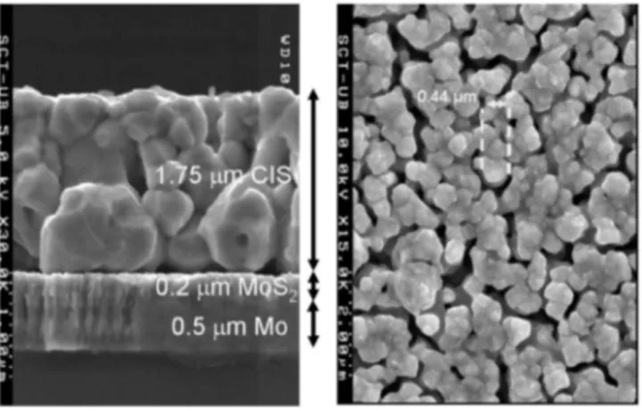
Figure 1 shows SEM pictures obtained from samples grown at the lowest temperature共Tnom= 550 ° C兲. In the cross section image the molybdenum coated glass substrates, onto which the absorber layers are formed, can be appreciated. In this case, the CuIn共S,Se兲2 phase exhibits a polycrystalline microstructure with a quite large dispersion in the grain size, which varies roughly from 100 nm to 1 m. Even though the film appears compact, it is still possible to appreciate the presence of some voids. The poor compactness of the sample is more evident in the top view SEM image of this sample, where it can also be observed that the grains tend to group, forming cluster structures. This microstructure is a direct re-sult of the annealing process, which on the one hand pro-motes the sulfurization and growth of the nanometric precur-sor crystallites, and on the other hand favors the coalescence of the grains. However, it can be observed that in the case of the sample processed at 550 ° C, the thermal energy provided by the annealing process is not able to completely recrystal-lize the clusters, which finally results in the presented micro-structure. Furthermore, the cross section image also reveals the presence of an intermediate layer between the Mo and the CuIn共S,Se兲2 ones. The estimated thickness of this layer is
about 200 nm and presents a characteristic and distinctive columnar structure. This layer has been found to be consti-tuted primarily by MoS2, as will be shown in the next
sec-tions.
FIG. 1. SEM cross section共left兲 and top view 共right兲 images obtained from the precursor annealed at the lowest temperature共Tnom= 550 ° C兲.
The effect of increasing the annealing temperature on the film morphology can be observed in Fig.2. The most notice-able effect is the increase in the average grain size 共above 1 m兲 and film compactness. Moreover, a second important effect is the increase in the thickness of the MoS2 interme-diate layer which, according to the cross section images, at-tains a total thickness of the order of 1.2 m.
B. Raman/AES measurements
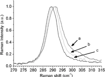
Raman spectra were obtained from the surface of samples annealed at three different temperatures共see Fig.3兲. In principle, the main peaks in the Raman spectra from CuIn共S,Se兲2 correspond to the A1 symmetry zone-center
phonon band of the chalcopyrite structure that shows a bi-modal behavior with two bands involving pure S–S and Se–Se vibrations.5 The spectra measured in the samples are characterized by a dominant peak, which corresponds to the S–S vibrational mode. The position of this band is close to the reference position obtained from a CuInS2 single crystal
共290 cm−1兲. This indicates that during the annealing process
sulfur replaces most of the selenium atoms originally present in the precursor nanocrystals. Nevertheless, the different sul-furization temperature is responsible for notorious
differ-ences in the spectra: As shown in Fig.3, decreasing the tem-perature of sulfurization leads to a blueshift and an asymmetric broadening of the peak, with an increase in the contribution at higher wavenumbers. As will be discussed in the next sections, these effects have been attributed to an increase in the density of crystalline defects in the samples annealed at lower temperatures.
Due to the exceptionally high absorption coefficient of CuInS2, the information provided by surface Raman analysis
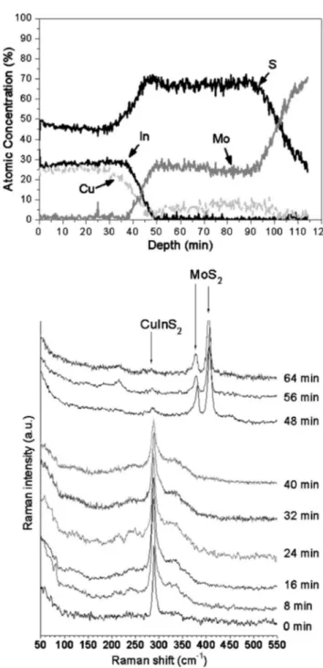
is restricted by the penetrating light in the material to the first 100 nm of the film. Nevertheless, the chemical and crystal-line properties of the bulk of the films can be assessed by using ion sputtering to etch the surface of the film. This procedure has been systematically carried out by combining Raman and AES measurements, as described in the experi-mental section. Figure4 shows the Raman spectra and AES compositional depth profile for a sample grown at Tnom
= 550 ° C. AES profiles show a bulk stoichiometry close to CuInS2, with a slightly Cu depleted region only on the film
surface. Such deviation appears to be characteristic of CuIn共S,Se兲2 compounds and has been associated in the lit-erature with an accumulation of a high number of vacancies leading to the presence of ordered vacancy compound sec-ondary phases on the surface region of the layers.6,7 Further-more, Raman spectra from the bulk of the sample confirm that the film is constituted by chalcopyrite ordered CuInS2,
even though the crystalline quality of this phase worsens toward the back interface, as can be appreciated by a signifi-cant broadening of the A1 band. The Raman spectra mea-sured in this region also show a broad contribution in the 320– 360 cm−1 spectral range. This could be related to the presence in the layers of CuIn5S8domains.8Approaching the
Mo back region, two bands clearly emerge in the spectra at 378 and 403 cm−1. These bands prove the formation of a
MoS2 intermediate layer during the sulfurization process.9
The existence of this phase is also noticeable in the AES profiles, which show a sulfur enrichment in the region where the Mo signal starts to grow. In addition, AES profiles also reveal the accumulation of Cu immediately above the MoS2 intermediate region.
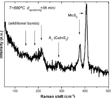
The samples grown at Tnom= 680 ° C present a similar bulk compositional profile with a slight In-rich composition, as shown in Fig.5. Deconvolution of the bulk Raman spectra reveals that the width of the A1chalcopyrite band is smaller in the case of the sample grown at the highest temperature, which indicates that the crystalline quality of the chalcopy-rite phase is improved by higher annealing temperatures. The spectra measured in this region also show a broad contribu-tion at the 320– 360 cm−1 region that could be indicative of
the presence of the CuIn5S8spinnel secondary phase. On the
other hand, it is worth noting the increase in the thickness of the MoS2 intermediate layer between the absorber and the
Mo ones, which is evidenced in the AES profile. In this case, this intermediate layer shows a significant content 共in the range of 5%–10%兲 of Cu. This is also accompanied by a significant decrease in the Cu content in the region of the absorber close to the interface of the MoS2layer. The Raman
spectra from this layer are characterized by the presence of the bands’ characteristic of pure MoS2 appearing close to
FIG. 2. SEM cross section共left兲 and top view 共right兲 images obtained from the precursor annealed at the highest temperature共Tnom= 680 ° C兲.
FIG. 3. Raman spectra obtained from the surface of the three samples an-nealed at different nominal temperatures:共a兲 550 °C, 共b兲 600 °C, and 共c兲 680 ° C.
their reference position. Accordingly, no indications of Cu alloying within the MoS2 are observed in the spectra.
Fur-thermore, some low intensity bands arise in the spectra close to the interface region共145, 185, and 213 cm−1兲, which may be directly related to the presence of Cu observed in the AES profiles共see Fig.6兲. These bands are tentatively attributed to a Cu-rich phase, though we have not been able to assign them to any referenced compound in the literature. The iden-tification of the origin of these modes requires a further analysis of these layers.
C. X-ray diffraction measurements
Figure 7 shows the 2/ diffractograms obtained from the samples grown at highest and lowest temperatures 共680
and 550 ° C, respectively兲. The diffractograms clearly indi-cate the presence of the cubic Mo phase, with a quite clear texture in the 共110兲 direction. In addition, they also contain reflections characteristic of the chalcopyrite structure of the CuInS2 compound, with a slightly preferential texture in the
共112兲 direction. An interesting difference between the two diffractograms deals with the presence of additional tions at 32.8°, 58.3°, 68.7°, and 96.7°. Initially, these reflec-tions were attributed to the presence in the layers of CuIn5S8
and CuIn5S9phases. This was done from the analysis of the
samples grown at the highest temperature, taking into ac-count the slightly In-rich composition of the absorbers and the evidence in the in-depth Raman spectra, suggesting the presence of CuIn5S8.3 However, the analysis of a broader
ensemble of samples has allowed the observation of a direct FIG. 4. AES depth profile共top兲 and Raman spectra measured at different
depths共bottom兲 from the sample annealed at Tnom= 550 ° C.
FIG. 5. AES depth profile共top兲 and Raman spectra measured at different depths共bottom兲 from the sample annealed at Tnom= 680 ° C.
correlation of the intensity of these reflections with the thick-ness of the intermediate MoS2layer. This leads to the
assign-ment of these relatively broad bands to the 共101兲, 共110兲, 共021兲, and 共211兲 reflections of MoS2. The relative intensity
of these peaks in the diffractograms suggests the presence of the rhombohedral 共R3m兲 MoS2phase. However, taking into
account the strong similarities between the XRD diffracto-grams from both rhombohedral and hexagonal phases of MoS2, the presence of the hexagonal MoS2 phase in the
samples cannot be excluded. The assignment of these bands to this compound is also supported by-scan measurements, which show that their intensity increases close to the inter-mediate region between the absorber and the back Mo con-tact. Moreover, the absence of a 共003兲 reflection points out that MoS2 grows preferentially with the c axis of the
crys-tallographic structure parallel to the surface.
IV. DISCUSSION
The changes observed in the main A1 CuInS2 mode in
the Raman spectra from the samples sulfurized at different temperatures are related to the presence of crystalline defects in the absorbers: Lower annealing temperatures produce films with higher density of crystalline defects, which lead to shorter phonon lifetimes in the crystals. As a result, the band-width of the A1band is substantially larger in the case of the samples obtained at lower temperatures. Furthermore, the lower crystalline quality of samples processed at lower tem-peratures has two additional effects on the spectra. First, it induces a clear asymmetry in the A1band. Second, it leads to a gradual 共blue兲 shift of the A1 band toward higher
wave-numbers. XRD stress measurements reveal the presence of stress levels in the chalcopyrite phase from the different samples close to the uncertainty of the measurements, with FIG. 6. Raman spectrum obtained from the bulk of samples annealed at
Tnom= 680 ° C after a sputtering time of 54 min, showing the presence of additional bands that may be related to a Cu-rich phase.
compressive stress values in the 10–50 MPa range. These stress values are too low to explain the observed shift of the Raman band. Furthermore, both effects共blueshift and asym-metric broadening of the A1 peak兲 are interpreted as direct results of the higher density of crystalline defects present in samples annealed at lower temperatures. The presence of de-fects relaxes the momentum conservation rule in the crystal, thus making possible the participation of noncenter phonons in the Raman process. As a result, the line shape of the Ra-man peak is ultimately determined by the number of defects, the density of states of phonons, and the shape of phonon dispersion curves. This is supported by a theoretical calcula-tion of the A1CuInS2dispersion curves, which show a posi-tive slope in the vicinity of the ⌫ point of the Brillouin zone.10,11 Then, the blueshift and band asymmetry toward high wavenumbers are basically a consequence of this posi-tive slope of the dispersion curves of the A1band close to the
center of the Brillouin zone.
The presence of a higher density of defects in the samples sulfurized at lower temperatures is also accompa-nied by a significant decrease in the open circuit voltage 共Voc兲 in the solar cells, from values of 0.75 V 共sample
sulfu-rized at Tnom= 680 ° C兲 down to 0.66 V 共sample sulfurized at
Tnom= 550 ° C兲. This is related to the dependence of Vocon
the density of defects acting as recombination centers in the space charge region of the devices,11,12 which are also con-tributing to the activation of noncenter phonons in the Ra-man spectra. This, together with the worsening of the layer crystallinity, contributes to the observed decrease in the effi-ciency of the devices: Cells fabricated with absorbers syn-thesized at the highest temperature of 680 ° C have typical efficiency values of⬃8.5%, and this parameter decreases down to ⬃6% when the temperature of sulfurization de-creases down to 550 ° C.
On the other hand, increasing the sulfurization tempera-ture also favors the growth of a thicker intermediate MoS2
layer between the absorber layer and the back Mo contact. In principle, the presence of this phase is desirable in terms of avoiding the formation of a rectifying union in the back con-tact. Evidence on the presence of a very thin interfacial MoS2 layer region have also been reported for CuInS2 ab-sorbers synthesized using conventional vacuum based processes,9,13this being similar to the thin interfacial MoSe2 layer observed at the back region from Cu共In,Ga兲Se2
absorbers.7 In relation to these works, the electrodeposited samples are characterized by the presence of a thicker MoS2 interfacial layer. This is specially true for the samples sulfu-rized at the highest temperature, where the thickness of the intermediate MoS2 layer becomes comparable to that of the
absorber. This could be favored by the preferential growth of this layer with the c axis of the crystallographic structure parallel to the surface, according to the XRD data. In this sense, the higher diffusivity of Cu in crystalline directions perpendicular to the 共003兲 one would allow the synthesis of thicker MoS2layers, this behavior being enhanced at higher
sulfurization temperatures. The presence of a thick MoS2
layer could contribute to an increase in the serial resistance of the solar cell device, thus degrading its performance.
However, in spite of this behavior, the analysis of the
I共V兲 characteristics of the devices measured under
illumina-tion shows similar values of the serial resistance of cells fabricated with absorbers sulfurized at different tempera-tures, which is kept at around 4.5 ⍀ cm2. This suggests that
the increase in the thickness of the MoS2 layer does not
contribute to the increase in the serial resistance of the de-vice. Then, the decrease in the efficiency of the devices sul-furized at lower temperatures is mainly related to the de-crease in Vocand the fill factor, which would be determined
by the presence of a higher density of structural defects in the absorbers, as suggested by the Raman spectra. This also correlates with the existence of significant changes in the composition of the interface region between the absorber and the MoS2 one, which can also contribute to the observed
variations in the parameters of the solar cell devices. Lower sulfurization temperatures lead to an interface region with a high Cu content, as shown in the in-depth AES composition profiles. This correlates with the existence of a Cu excess in the interface region between the CuInSe2 electrodeposited
absorbers and the back Mo layer.14After annealing, it is not clear whether this Cu excess is accommodated inside the chalcopyrite structure, or it indeed corresponds to a segrega-tion of a binary CuxSy compound. The absence of covellite
共CuS兲 characteristic bands in the Raman spectra excludes the presence of this phase, which is known to yield intense bands at 19 and 475 cm−1.15
However, the complexity of the Cu–S phase diagram makes it difficult to exclude the presence of other phases with lower Raman signals, such as Cu3S2,
Cu2−xS, and CuS2. Increasing the temperature of
sulfuriza-tion favors diffusion of Cu into the thicker MoS2 layer,
which likely determines the formation of a Cu depleted in-terface region. This could also be favored by a higher surface segregation of excess Cu in the form of Cu-rich secondary phases.3This implies the need to improve the knowledge of the structural composition of the film close to the back con-tact in order to precisely model the performance of solar cell devices based on these absorbers.
V. CONCLUSIONS
In this paper we have investigated the effect of the an-nealing temperature on the crystalline properties of CuInS2 films obtained from the sulfurization of electrodeposited CuInSe2 nanocrystalline precursors and their impact on the solar cell characteristics. Higher sulfurization temperatures lead to films with improved crystallinity and larger average grain size. However, it also favors the formation of a thicker MoS2 interphase layer between the CuInS2 absorber layer
and the Mo back contact, as supported from the SEM, Ra-man, AES, and XRD measurements. The analysis of the I共V兲 characteristics of the solar cells shows a decrease in the ef-ficiency of the devices fabricated with the absorbers sulfur-ized at lower temperatures. This is related to the worsening of the layer crystallinity and the increase in the density of structural defects共as deduced from the Raman spectra兲 ob-served when the temperature of sulfurization decreases. On the other hand, the degradation of the solar cell parameters also correlates with an accumulation of Cu close to the MoS2
this Cu excess may be responsible for the apparition of uni-dentified additional bands in the Raman spectra from the bulk of the samples. This suggests the need to improve the degree of control of the structure and composition of the interface region between the absorber and the back MoS2
layer, in addition to the crystalline quality of the absorber, for the optimization of the efficiency of the devices.
ACKNOWLEDGMENTS
EME is a member of CEMIC共Centre of Microsystems Engineering兲 of the Generalitat de Catalunya. This work was funded by the LARCIS project 共Grant No. SES6-CT-2005-019757兲 of the Sixth FM Programme of the European Com-mission.
1M. A. Contreras, K. Ramanathan, J. AbuShama, F. Hasoon, D. L. Young, B. Egaas, and R. Noufi,Prog. Photovoltaics13, 209共2005兲.
2D. Lincot, J. F. Guillemoles, S. Taunier, D. Guimar, J. Sicx-Kurdi, A. Chaumont, O. Roussel, O. Ramdani, C. Hubert, J. P. Fauvarque, N. Bo-dereau, L. Parissi, P. Panheleux, P. Fanouillere, N. Naghavi, P. P. Grand, M. Benfarah, P. Mogensen, and O. Kerrec,Sol. Energy77, 725共2004兲. 3V. Izquierdo-Roca, A. Pérez-Rodríguez, A. Romano-Rodríguez, J. R.
Mo-rante, J. Álvarez-García, L. Calvo-Barrio, V. Bermudez, P. P. Grand, O. Ramdani, L. Parissi, and O. Kerrec,J. Appl. Phys.101, 103517共2007兲. 4L. Calvo-Barrio, A. Pérez-Rodríguez, J. Álvarez-García, A.
Romano-Rodríguez, B. Barcones, J. R. Morante, K. Siemer, I. Luck, R. Klenk, and R. Scheer,Vacuum63, 315共2001兲.
5R. Bacewicz, W. Gebicki, and J. Filipowicz,J. Phys.: Condens. Matter6, L777共1994兲.
6K. Müller, R. Sheer, Y. Burkov, and D. Schmeißer, Thin Solid Films 451–452, 120共2004兲.
7H. W. Schock and U. Rau, Physica B共Amsterdam兲 308–310, 1081 共2001兲. 8N. M. Gasanly, S. A. El-Hamid, L. G. Casanova, and A. Z. Magomedov,
Phys. Status Solidi B 169, K115共1992兲.
9J. Álvarez-García, A. Pérez-Rodríguez, A. Romano-Rodríguez, J. R. Mo-rante, L. Calvo-Barrio, R. Scheer, and R. Klenk,J. Vac. Sci. Technol. A 19, 232共2001兲.
10J. Lazewski, P. T. Jochym, and K. Parlinski,J. Chem. Phys.117, 2726 共2002兲.
11E. Rudigier, Ph.D. thesis, Philipps-Universität Marburg, 2004.
12V. Izquierdo, A. Pérez-Rodríguez, L. Calvo-Barrio, J. Álvarez-García, J. R. Morante, V. Bermúdez, O. Ramdani, J. Kurdi, P. P. Grand, L. Parissi, and O. Kerrec, Thin Solid Films, “Raman scattering microcrystalline as-sessment and device quality control of electrodeposited CuIn共S,Se兲2 based solar cells”共unpublished兲.
13R. Scheer and H.-J. Lewerenz,J. Vac. Sci. Technol. A13, 1924共1995兲. 14O. Ramdani, Ph.D. thesis, Université Pierre et Marie Curie共Paris 6兲, 2007. 15M. Ishii, K. Shibata, and H. Nozaki,J. Solid State Chem.105, 504共1993兲.