Analysis of geometrical effects on the behavior of transverse
and longitudinal modes of amorphous silicon compounds
J. A. Moreno, B. Garrido,a)J. Samitier, and J. R. Morante
Electronic Materials & Engineering laboratory (E.M.E.), Departament de Fı´sica Aplicada i Electro`nica, Universitat de Barcelona, Diagonal 645-647, 08028 Barcelona, Spain
~Received 24 June 1996; accepted for publication 12 November 1996!
The peak frequency, width, and shape of the transverse-optical~TO! and longitudinal-optical ~LO! infrared absorption modes of silicon oxides ~SiO2, SiOx!, silicon nitrides ~Si3N4, SiNx!, silicon
oxynitrides ~SiOxNy!, and other silicon compounds have often been connected with stress,
stoichiometry, defects, structural order, and other properties of the layers. However, certain geometrical effects strongly influence the spectral response of the material independent of its physical or structural properties. The influence of layer thickness, multilayer configuration, substrate effects, angles, and polarization on the behavior of TO and LO bands are presented and discussed. Some corrections are suggested to reduce experimental error and for the reliable measurement of stress, composition, disorder, and structure. © 1997 American Institute of Physics.
@S0021-8979~97!05104-9#
I. INTRODUCTION
Infrared transmission spectroscopy is widely used to ob-tain information about the composition and structure of di-electrics and semiconductors. In the study of the vibrational spectra, band parameters of transmission or reflection reso-nances such as peak frequency, width, shape, and intensity are correlated with the physical and microstructural proper-ties of the materials. For instance, in thin SiO2films, intrinsic stresses are often measured from the peak frequency of the transverse-optical ~TO! and longitudinal-optical ~LO! stretching modes of the Si–O bond ~TO3 and LO3, respec-tively! by using models applicable to the short-range order of the amorphous structure.1–3 Moreover, the composition and microstructure of nonstoichiometric silicon oxides, nitrides, oxynitrides, and other silicon compounds are frequently measured from the peak frequency, shape, and other features of the infrared bands.4–19Evaluation of the hydrogen content ~or other impurities! in deposited or grown amorphous layers are routinely determined from the intensity and position of their respective infrared resonances.20–22
Spectral variations are almost always assumed to be due to variations in physical properties of the layers and less frequently in the thicknesses of the layers, angle, and polar-ization of incident light and multilayer arrangement. The re-sults are usually coherent, especially when samples with similar thicknesses and in the same experimental conditions are compared. However, comparisons between the results obtained by different workers are always difficult because experimental values of peak frequencies, widths, and inten-sities of spectral bands are scattered over a wide range. A good illustration is provided by the study of stresses in ther-mal SiO2 layers. The peak frequency given for the TO3 ab-sorption of 400 Å thick layers after relaxation of the structure by annealing is around 1075 cm21. However, for relaxed oxides of 1000 Å, in principle with the same structure, the values reported are around 1083–1084 cm21; moreover, for
the same oxides but with thicknesses around 4000–5000 Å, the values reported, always after annealing, are in the range between 1090 and 1095 cm21. Obviously, there exist encies between samples originated exclusively from a differ-ent structure~the oxide close to the interface is denser due to the presence of a compressive stress13,14!, but one must be able to separate them from thickness and interference effects. Some previous studies have reported variations in the peak parameters of the spectra with the thickness of the lay-ers, mainly for SiO2.7,23–26In view of those particular modi-fications of the spectra, it is the purpose of this paper to quantify their magnitude and influence and to propose cor-rections to reduce their effects. The paper is organized as follows: First, we present a study of the bands generated with a computer simulation program that is based on the matrix formalism for field propagation through a multilayer system. Second, these results are compared with the experimental data obtained from the infrared analysis of thermal SiO2 lay-ers with different thicknesses grown onto silicon waflay-ers. Some results concerning silicon nitrides are also considered. Third, we propose an explanation of the origin of geometri-cal effects and the corrections that should be taken into ac-count. Finally, the equations for the reflection and transmis-sion coefficients on multilayer structures are developed in Taylor series with thickness as an independent variable to evaluate analytically the geometrical effects for thin layers.
II. GEOMETRICAL EFFECTS IN LAYERED SYSTEMS: SIMULATION ANALYSIS
For the optical study of multilayered materials we used the approach of Harbecke.27–30This method allows calcula-tion of the complex–amplitude refleccalcula-tion and transmission coefficients~r and t! for a pile of faced absorbent layers. The main goal of the procedure is that it is able to eliminate the interference fringes of thick layers from the concept of the coherent and incoherent multiple reflections within the lay-ers. Thus, in the model calculations it was possible to avoid the very narrow interferences of the thick silicon substrate.
The transformation of fields across the interface between two layers and the propagation inside each layer are considered from the well-known matrix formalism developed by Abele`s.27,28 If the multilayer consists of L parallel layers ~Fig. 1!, the final transformation of fields from right to left is the result of the product of 2L11 matrices, L11 interfaces for passing~@Mj#, j51,...,L11!, and L matrices for in-layer
propagation ~@Pj#, j51,...,L!. In the case of s polarization
~transverse electric wave!, we consider the propagation of the electric field E5~0,E,0!, which is parallel to the inter-faces. For p polarization ~transverse magnetic wave!, we consider the field H5~0,H,0!, now parallel to the interfaces. Then, for s polarization, when an electromagnetic wave Eiis projected on the pile, the reflected wave Erand the transmit-ted wave Etare connected with
S
Ei ErD
z5025@ML11#@PL#@ML#•••@P1#@M1#S
Et 0D
z 5z11 [S
T11 T21 T12 T22DS
Et 0D
z5z 1 1. ~1!The modifications for p polarization and the detailed expres-sions of the transformation matrices are given in the Appen-dix, and include the Fresnel’s coefficients, which depend on the complex dielectric functionsejof the materials. Thus, the complex–amplitude reflection and transmission coefficients of the whole pile are
r5Er Ei 5T21 T11 , ~2! t5Et Ei 5 1 T11 . ~3!
Finally, the reflection (R) and transmission (T) of the multilayer are given by
R5rr*, ~4!
T5Re@Nb#
cosa tt*, ~5!
where Nbis the generalized refractive index of the back me-dia~defined in the Appendix! andais the angle of incidence ~Fig. 1!.
The inputs to the simulation program were the complex dielectric functionsej~v! ( j51,...,L) of each layer. The op-tical properties of the materials are embodied ine~v! and its dependence on frequency. We assumed the materials to be composed of a set of dumped harmonic oscillators, one for each absorption mode. All the simulations were performed by using the results of two models for the frequency depen-dence of the dielectric function. ~i! model 1 ~three param-eters! is based on oscillator terms of the following structure:
e~v!5e`1
(
k 4pVk2 v0k 2 2v22ig kv , ~6!where k runs across the relevant vibration modes, Vk,v0k, andgkare, respectively, the oscillator strength, frequency of resonance, and dumping constant of the mode k, ande` rep-resents the polarizability due to electronic resonances. ~ii! model 2 ~four parameters! has an additional parameter,sk, which accounts for the dispersion in frequency of the oscil-lator strength of each mode ~the Gaussian distribution for symmetric peaks!. The oscillator terms have the following expression: e~v!5e` 1
(
k 1 skA
pE
0 ` 4pVk2 exp@2~C2v0k!2/sk 2# C22v22ig kv dC. ~7! Model 2 has been reported to reproduce the spectra of amor-phous materials such as SiO2and SiNx successfully.4,5 The two main options of the simulation program are~i! determination of dielectric functions from reflectance or transmittance measurements ~by a fitting procedure! and ~ii! simulation of reflection and transmission spectra for any multilayered system under various experimental conditions.25,31The results based on the model 1 and model 2 for thermally grown SiO2 and deposited Si3N4 layers are shown in Table I. These results were the input data to all the simulations performed in the present work and agree with similar calculations reported in the literature.26
We simulated the reflection, transmission, and absor-bance spectra of SiO2 and Si3N4 layers grown or deposited onto silicon wafers. The absorbance spectra of some SiO2 layers are shown for illustration in Fig. 2. Briefly, the stretch-ing band of SiO2 is composed of two TO modes: the TO3 mode is associated with the asymmetric stretching motion of the oxygens atoms of two adjacent Si–O–Si units, and its high-frequency shoulder~TO4mode!, which has been attrib-uted to the symmetric stretching motion of Si–O–Si adjacent units. The TO4mode has been related to the disorder in the amorphous structure of SiO2.
5
In thermal oxides, these modes are centered, respectively, around 1070–1090 cm21 and 1200 cm21. We have also studied their related longitu-dinal modes LO3 ~;1256 cm21! and LO4 ~;1160 cm21!, FIG. 1. Schematic representation of the model and coordinates used for the
which are excited under oblique incidence by the component of the electric field perpendicular to the sample surface ~p polarization!.5,32
After baseline subtraction33we determined the peak fre-quency, peak width, and intensity of the bands. We found large variation of these features with the thickness of the layer and angle of incidence of the radiation, though we did not vary the dielectric functions used as data for the simula-tion program. In Fig. 3 we show the variasimula-tion of the TO3
peak frequency as a function of the thickness of the layer for both reflection and transmission ~model 1!. In transmission, TO3 peak frequency for 100 Å thick samples is 1077 cm21, but for 6000 Å it is 1092 cm21. These variations are similar to those mentioned in the introduction to the experimental measurements reported in the literature. In the same range of thicknesses, the width of the TO3 mode ranges between 67 and 82 cm21. The evolution of the infrared band of Si3N4is similar, i.e., it shifts to higher frequencies as thickness in-creases. These results are compared with the experimental work presented in the next section.
Important modifications of the shape of the bands are also observed. For comparison, we have plotted the simu-lated absorption spectra of a SiO2layer of 100 Å and another of 6500 Å in Fig. 4; for comparison, the scales of the y axis for the two plots were normalized so that the height of both TABLE I. Parameters of the dielectric function for thermally grown SiO2
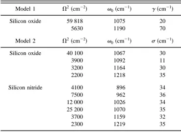
and deposited Si3N4layers. The values of model 2 for the oxide were
ob-tained after fitting the experimental reflection and transmission spectra. The values of model 1 for the oxide and model 2 for the nitride were extracted from literature~Refs. 4 and 30!. V,v0, andgare, respectively, the oscillator
strength, frequency of resonance, and dumping constant of the different modes. Model 2 has an additional parameter,s, which accounts for the dispersion in frequency of the oscillator strength of each mode. The best damping parameter for all the modes in model 2 was 8 cm21.
Model 1 V2~cm22! v0~cm21! g~cm21! Silicon oxide 59 818 1075 20 5630 1190 70 Model 2 V2~cm22! v 0~cm21! s~cm21! Silicon oxide 40 100 1067 30 3900 1092 11 3200 1164 30 2200 1218 35 Silicon nitride 4100 896 34 7500 962 36 12 000 1026 34 25 200 1070 35 3700 1159 32 2300 1219 35
FIG. 2. Simulated absorbance at 45° of incidence of SiO2 layers on Si
substrate for different thicknesses~model 2!. The intensity increases with the thickness of the layer~100 Å, 500 Å, and from 1000 to 9000 Å in steps of 1000 Å!. The peak frequencies of the transverse optical modes ~TO3and
TO4! and the longitudinal optical modes ~LO3and LO4! are indicated.
FIG. 3. Peak frequencies of the TO3band of SiO2on Si as a function of the
thickness of the layer, for simulated reflection and transmission spectra.
FIG. 4. Comparison between simulated absorption spectra at normal inci-dence of SiO2on Si for different thicknesses: 100 Å in~a!, and 6500 Å in
peaks was the same. The frequency shift of the TO3mode is evident, as is the greater high-frequency shoulder of the thicker sample ~TO4 band!. Such dependence on thickness prevents us from indiscriminately analyzing the behavior of the TO4band for quantifying disorder effects. The TO4mode is nearly absent of the spectra of the very thin SiO2 layers ~less than 50 Å!. Lange6,9
did not find experimentally this shoulder for very thin samples, and other authors speculated about this fact.12,25,34In the experimental spectra of very thin layers, superimposed to these effects there are obvious modi-fications of the structure, as the interface of SiO2 with the silicon substrate is far from being abrupt.
We found that the frequency and width dependence of the peaks on the angle of the incident radiation is not signifi-cant. In contrast, the intensities of both TO and LO peaks are strongly dependent on the angle of incidence in the following way. For SiO2 absorbance spectra, we found that the inten-sity of LO modes increased monotonically with the angle of incidence @Fig. 5~a!#. However, the behavior observed for reflection was unexpected: the LO intensity first increased, reached a maximum at approximately 45°, then decreased and changed in sign ~negative peaks! between 60° and 65° @Fig. 5~b!#. This inversion in the sign of the LO mode was found around the Brewster angle for silicon ~72°!; at this value, the reflection coefficient of the p wave at the silicon interface~which excites the LO mode! vanishes. Thus, large incident angles aid detection of LO bands ~but far from the inversion point, see Fig. 5!. However, the intensity of TO bands always decreased with the angle of incidence.
The dependence of the TO3peak frequency on thickness for oblique incidence was similar to that for normal inci-dence. In contrast, irrespective of the angle of incidence
taken, the LO3 peak frequency changed only slightly ~2–3 cm21! within the whole range of thicknesses studied ~100– 6000 Å!. Unfortunately, the LO3 mode also shows little variation with stress, composition, and microstructure.3,7,25
We also found similar spectral behavior for the simu-lated stretching bands of silicon nitride on silicon substrates. Peak frequencies and widths increased with thickness as for SiO2, so this behavior is expected to be quite general. Some experimental data on silicon nitrides are shown to correlate with the simulation results, as will be shown later.
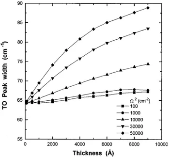
With the aim of studying these geometrical effects on infrared bands in a more general way, several single bands ~model 1! for different oscillator strengths were given as in-put data in to the simulation program. Then, the reflectance and transmittance spectra generated were analyzed as a func-tion of the thickness of the layers. The most striking finding was remarkable differences in behavior depending on the oscillator strength. For strong bands, the behavior of peak frequency and width was similar to that reported above for SiO2, but for weak bands, for example, impurity bands such as the Si–H or N–H absorptions, the variation with thickness was less pronounced, and the asymptotic limit was much lower ~Figs. 6 and 7!.
Interference fringes for thick layers tend to distort spec-tral features, so a baseline specspec-tral subtraction should be per-formed by reproducing the oscillating background.33 It can then be shown that the intensity of TO bands is linear with thickness in a wide range of thickness variation. In contrast, the intensity of the LO modes is linear for small thicknesses, but the slope of the curve changes ~Fig. 8!. Therefore, only the TO modes of the infrared spectra are suitable for thick-ness evaluation.
III. EXPERIMENTAL PROCEDURE
For the experiments, the samples used were 8000 and 2500 Å thick silicon oxide layers on silicon,100. wafers FIG. 5. ~a! Intensity of the LO3 mode of SiO2 in absorbance
~2log@transmittance#! as a function of the angle of incidence. ~b! The same
in reflection~2log@reflectance#!.
FIG. 6. TO peak frequency as a function of thickness for absorbance spectra at normal incidence, simulated from a dielectric function with a single mode
~model 1!. The curves are parametrized for different oscillator strengths ~V!
of the mode. The other parameters given as data for the simulation, where v051000 cm21andg530.
with resistivity between 3 and 5 V cm. The layers were grown by wet oxidation at 950 °C and annealed at 1100 °C in a rapid thermal annealing system for 10 s. The other thick-nesses were obtained after etching those layers in a buffered HF solution and measuring the remaining film thickness with optical interferometry by using a Nanospec AFT 200 of Na-nometrics. For each etch step we averaged at least four thick-ness measurements taken at different points on the wafer. Before the infrared experiments, the oxide on the back of the wafers was etched off. The silicon nitride layers were
ob-tained in a low-pressure chemical vapor deposition system from SiH4and NH3as precursor gases. The deposition time was adjusted to obtain a suitable range of thicknesses, which were subsequently measured by ellipsometry.
The infrared measurements were performed with a BOMEM DA3 series Fourier transform infrared spectropho-tometer with accessories to work in transmission and reflec-tion at normal incidence or at incident angles between 20° and 80°. The resolution limit was 1 cm21 and at least 400 scans were averaged for each measurement. The infrared source was a globar, the beamsplitter of KBr and the detector was a high-sensitivity mercurium–cadmium–telluride ~MCT! cooled by liquid nitrogen. From the single beam in-frared spectra of the samples, we subtracted the spectra of the bare silicon references to eliminate silicon absorption components. Depending on layer thickness, an oscillating background was superimposed to the spectra ~layer interfer-ences!, then a procedure to subtract this background was followed.33As a result, flat base lines were accomplished for all the samples, irrespective of their thickness.
IV. EXPERIMENTAL RESULTS
The experimental values of the peak frequencies of the TO3silicon oxide absorption mode versus thickness are plot-ted in Fig. 9, together with the results of the simulation analysis. The full curve accounts for the results predicted from simulation by using model 1. The dashed curve repre-sents the results obtained from model 2. Model 2 closely reproduces the experimental results for the whole range of thicknesses, except for the two thicker samples ~4600 and 8000 Å!, where some differences occur. The origin of these differences will be discussed later. The results of the band-width for the TO3mode are plotted in Fig. 10. Model 2 also reproduces the experimental results more closely, suggesting that it is more suitable for the analysis of amorphous mate-rials. Furthermore, the shape of infrared bands obtained from model 2 better reproduced the experimental ones. The ex-FIG. 7. TO peak width as a function of thickness for absorbance spectra at
normal incidence, simulated from a dielectric function with a single mode
~model 1!. The curves are parametrized for different oscillator strengths ~V!
of the mode. The other parameters given as data for the simulation where v051000 cm21andg530.
FIG. 8. Intensity of TO and LO modes as a function of thickness for simu-lated absorbance spectra at 45° of incidence of SiO2layers on Si. It is clear
that only TO modes are linear through the whole range of thicknesses stud-ied.
FIG. 9. Experimental TO3peak frequency for absorbance at normal
inci-dence as a function of the thickness of the SiO2layer~triangles!. Simulated
behavior taking model 1~full line! and the model 2 ~broken line! for the dielectric function. Experimental data are very close to the predictions of model 2.
perimental peak frequencies for silicon nitride were also in agreement with the results of the simulations~Fig. 11!.
The reflection spectra of SiO2 measured with different angles of incidence are plotted in Fig. 12. The most impor-tant effect is the band distortion and inversion of the LO peak at around 60°, which was predicted above. The experi-mental inversion of the LO peak in SiO2at increasing angles of incidence was reported previously by other authors.35 V. DISCUSSION
In the previous sections we demonstrated, by both simu-lation and experiment, geometrical or optical effects in the study of the infrared spectra of multilayered systems.
More-over, we showed that simulation and experiment correlate well in a wide range of thicknesses, in different materials, and for both reflection and transmission spectra. However, we have not discussed the origin of these effects, nor yet given any procedure to sort out this dilemma. These effects are because the absorption spectrum is not an intrinsic prop-erty of the material, as is the dielectric function. However, the calculation of frequency dependence of the dielectric function is difficult without sophisticated software and some previous knowledge of the optical constants.
The origin of these effects in layered systems is due to two main factors. First, we have to distinguish the problem of the boundaries and the interference effects of the partial beam intensities. The transformation of fields across the in-terface between two layers is given by the Fresnel coeffi-cients, which depend on refractive indexes, extinction coef-ficients, and the angle of incidence. They give the fraction of the light that is transmitted or reflected across the boundary, and from their dependence they will mainly be influenced by the polarization and the angle of incidence of the incoming wave. Thus, polarization and angle effects on the spectra have their origins in the boundary conditions for the field across an interface. Then, the intensity of signal obtained from the TO and LO modes strongly depends on angles and polarization as we have reported above, predicting the dis-tortion and inversion of the LO mode in reflection.
Alternatively, interference within the layers gives a sinu-soidal base line dependence ~Fabry–Perot resonances!. Ob-viously, for multilayered systems, the equations governing the interferences are more complicated. The frequency of these background interferences is strongly dependent on the thickness of the layer ~quicker interferences for thicker lay-ers!, which has a complicated effect on the peak frequency, width, and shape of the absorption bands. Nevertheless, it can be argued that if this sinusoidal base line could be repro-duced exactly ~for example, by means of a simulation pro-gram!, then we would be able to subtract it from the experi-mental spectrum and so obtain the spectra without geometrical modifications. In fact, Maley33 proposed a FIG. 10. Experimental TO3peak width for absorbance at normal incidence
as a function of the thickness of the SiO2layer~triangles!. Simulated
behav-ior taking model 1~full line! and the model 2 ~broken line! for the dielectric function. Experimental data are very close to the predictions of model 2.
FIG. 11. Experimental silicon nitride peak frequency for absorbance at nor-mal incidence as a function of the thickness of the layer~squares!. The full line corresponds to the simulated results.
FIG. 12. Experimental reflection spectra of SiO2layers obtained at different
angles of incidence.~a! 30°, ~b! 40°, ~c! 50°, and ~d! 60°. The inversion of the LO3mode is clearly observed.
method to reproduce closely the sinusoidal interferences by setting the extinction coefficient (k) equal to zero and opti-mizing the refractive index (n) and the thickness (d) of the layer in the exact equations of the multilayered-system. However, this is only approximate because the refractive in-dex varies largely in the range of passing through absorbing bands, and then any constant parameter for fitting, even op-timized, cannot reproduce the shape of the base line. Other-wise, to determine the variation of n over the absorbing band requires the knowledge of the frequency dependence of the dielectric function, which is rather difficult, as we mentioned above. The total variation of the real part of the dielectric function through an absorbing band is connected with their respective oscillator strength values,Vj, and is given by the
sum rule Vj
252
p
E
band jne9
j~n!dn. ~8!
As an illustration representing the variation of n and k through an absorbing band, we have plotted the real (n) and imaginary (k) parts of the complex refractive index of SiO2 in the frequency range of interest ~TO3–TO4 mode! in Fig. 13. The calculations were performed by using the dielectric function generated from the parameters shown in Table I and taking into account that (n1ik)25e. Thus, any constant value for n taken over this region can only give approximate results for reducing the degree of band deformations.
Nevertheless, shifts and distortions of the spectra also depend on the intensity of the absorption band. Strongly ab-sorbing bands~i.e., high oscillator strength, V! lead to higher deformations when the thickness increases. Thus, main
infra-red bands for silicon oxide or silicon nitride, which are very strong, result in greater shifts and deformations than less intense bands such as impurity bands ~Si–H, N–H, etc.!. Figures 6 and 7 show that the slope of the curves for low oscillator strengths is lower than that for intense bands, clearly indicating smaller shifts and deformations of the in-frared spectra. The explanation of this behavior is also con-nected with the variation of n over the absorbing band and, thus, with the modification of the base line. In fact, stronger bands have higher variations of n in the absorbing region @Eq. ~8!#, and so, good base lines are more difficult to repro-duce with only one constant value of n.
It is important to remark that we took into account co-herent multiple reflections in the film and incoco-herent mul-tiple reflections in the substrate. This is important since in-coherence rules out the interference fringes. Therefore, as experiment and simulation gave very close results, this is a good choice for layers with thicknesses in the limit d!l. However, for thicker layers ~of the order of mm! the thick-ness begins to be comparable to the wavelength~midinfrared range is 400–4000 cm21or 25–2.5mm! and the behavior is neither coherent or incoherent. This is probably the reason why the experimental points of the two thicker layers of Fig. 9 do not reproduce the simulation behavior and deviate slightly from the simulated curve, which applies only at the coherent limit.
From the results presented above it is clear that some corrections must be taken into account for comparing the vibrational properties of samples with different thicknesses and/or different experimental setup. It is difficult to give only one expression for correcting these effects because the be-havior depends on the oscillator strength of the absorption being studied and, thus, on the sample itself. As discussed above, the best procedure would be to obtain the dielectric function after fitting the experimental spectra. If this is not possible, the best choice is to extrapolate peak frequencies and widths of the infrared bands to the limit of zero thick-ness. The absorbance position when thickness tends to zero coincides with the maximum of the dielectric function. This is in accordance with the fact that for very thin layers, ab-sorption spectra resembles the imaginary part of the dielec-tric function.25 Nevertheless, such extrapolation requires knowledge of the dependences on thickness, so simulation studies should be performed at least once to obtain the de-sired dependence for a given material. If simulation is not available, the general dependences versus thickness given in Fig. 6 can be used, provided the oscillator strength of the absorption is known.
We have fitted the peak frequency of SiO2 and Si3N4 layers with quadratic polynomials in d ~error less than 3%!. The corrections to zero thickness can be performed by sub-tracting from the experimental values the calculated values of the terms in Eq.~9! or Eq. ~10! that depend on d ~i.e., the sum of the linear and quadratic terms!. The following equa-tions are valid for transmission at normal incidence in a wide range of thicknesses~d in mm and valid up to 1mm!:
vmax~SiO2!51070.98165.07d25.3631023d2
~cm21!, ~9!
FIG. 13.~a! Real (n) and ~b! imaginary (k) parts of the refractive index of silicon oxide from the parameters of Table I~model 2!.
vmax~Si3N4!5830.60111.41d14.1631023d2
~cm21!. ~10!
These corrections were successfully applied by us to evaluate the infrared data in analyzing thin silicon oxides,7 in the study of implanted oxides,8,25 and in the analysis of buried oxides, where we found pronounced effects depending on the depth of the buried layer and the size in general.23,24 VI. ANALYTICAL APPROXIMATIONS FOR THE REFLECTANCE AND TRANSMITTANCE OF VERY THIN FILMS
Some of the previous results can be clearly understood if analytical approximations for the multilayer optics are devel-oped. The formulae for the transmission and reflection are complex even for a system composed of a thin layer and a substrate. Many authors proposed analytically exact or ap-proximate formulae for a single layer on a substrate under normal or oblique incidence.36,37 Developing approximate expressions giving the explicit dependence of transmission and reflection on the thickness of the layer is useful for our purposes.
After developing Eqs. 1–3 for only one layer on a sub-strate, the transmission (t) and reflection (r) coefficients of
the system, respectively, take the following form:27
t5 2 cosa
~cosa1hb!cos Nd2i~h1hb cosa/h!sin Nd
, ~11!
r5~cosa2hb!cos Nd1i~h2hb cosa/h!sin Nd
~cosa1hb!cos Nd2i~h1hb cosa/h!sin Nd
, ~12! where the subscript b stands for the substrate, d52pd/l is
the optical path inside the layer, N is the generalized refrac-tive index of the layer,ais the angle of incidence, andh5N for s polarization orh5N/efor p polarization. The reflection (R) and transmission (T) of the system are calculated from the coefficients in Eqs. ~11! and ~12! by using Eqs. ~4! and ~5!, and result in complicated expressions dependent on thicknesses, refractive indexes, angle, and dielectric func-tions of the layer and the substrate.
We discuss the expressions for first and second order in
d, which are obtained after developing the equations of T and
R in Taylor series. The result of these approximations for
first order ~very thin layers compared with wavelength! are given by the following equations:
Tpol s5 4Nb cosa ~cosa1Nb! 2
H
12 2 Im~e! cosa1Nb dJ
, ~13! Tpol p5 4Nb cosa ~cosa1Nb/eb!2H
122@Im~21/e!sin 2 a1Im~e!~N b/eb!cosa# cosa1Nb/eb dJ
, ~14! Rpol s5S
cosa2Nb cosa1NbD
2H
114 cosa Im~e! eb21 dJ
, ~15! Rpol p5S
cosa2Nb/eb cosa1Nb/ebD
2H
124 cosa @2Im~21/e!sin2 a1~N
b/eb!2 Im~e!cos2 a#
cos2 a2~Nb/eb!2 d
J
. ~16!The transmission and reflection of the layer for s polar-ization ~Tpol s and Rpol s! take, respectively, their minimum and maximum values ~absorption peaks! at a maximum value of the imaginary part of the dielectric function, Im~e!, i.e., at the poles of the dielectric function that are related to the TO modes. However, for p polarization there are addi-tional terms dependent on Im~21/e! so, other maxima or minima occur in Tpol p and Rpol p when Im~21/e! is in its maximum, i.e., at the zeros of the complex dielectric func-tion that are related to the LO modes.5,27,32Both LO and TO modes are affected by angular factors. If, for simplicity, we take the substrate as the vacuum, the angular dependence of the intensity of the LO and TO modes in Tpol pis TO}cosa and LO}~sina!2/cosa. Therefore, for normal incidence the intensity of LO modes is zero. Furthermore, by analyzing the angular dependence of the LO modes in Rpol p @Eq. ~16!#, it is easy to find that the term responsible for the inversion of
the LO modes is~cosa2Nb/eb!, which changes sign at the
Brewster angle of the substrate; so, the inversion of the LO modes and the angular dependence of TO and LO modes arise as a consequence of the substrate refractive index and are independent of the thickness and refractive index of the layer for very thin layers. This is in agreement with the re-sults of the simulation and the experimental rere-sults reported above.
The transmittance for s polarization @Eq. ~13!# depend linearly on Im~e! and then the transmission spectra of thin layers are similar to the frequency dependence of the imagi-nary part of the dielectric function. So, we can use these expressions to obtain approximate values of Im~e! at the limit of very thin layers. If we refer to the quotient between
Tpol s and the common factor in Eq.~13! ~transmittance of the substrate! as TRS, then
e
9
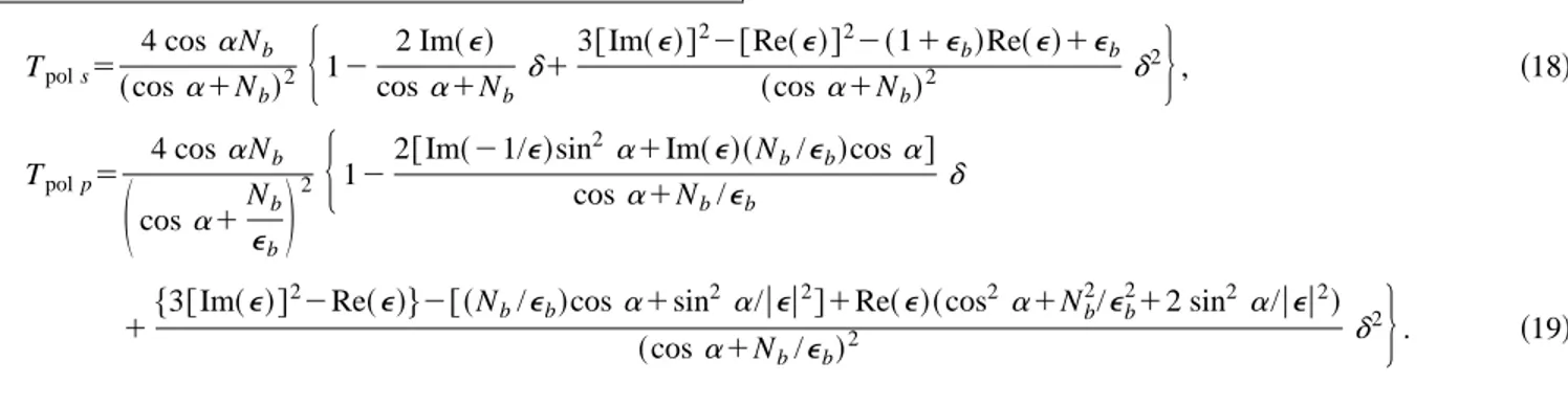
5Im~e!5~12TRS!~cos2d a1Nb!. ~17! The dielectric function in the infrared range can be ob-tained by this method within an error of 10% in a range ofthicknesses up to 500 Å. With the aim of evaluating second-order effects, we also developed the formulae for thed2term. The results obtained for transmission under s and p polariza-tion are Tpol s5 4 cosaNb ~cosa1Nb!2
H
12 2 Im~e! cosa1Nb d13@Im~e!#22@Re~e!#22~11eb!Re~e!1eb
~cosa1Nb!2 d 2
J
, ~18! Tpol p5 4 cosaNbS
cosa1Nb ebD
2H
122@Im~21/e!sin2 a1Im~e!~Nb/eb!cosa#
cosa1Nb/eb d
1$3@Im~e!#
22Re~e!%2@~N
b/eb!cosa1sin2 a/ueu2#1Re~e!~cos2 a1Nb
2
/eb212 sin2 a/ueu2!
~cosa1Nb/eb!2 d
2
J
. ~19!Finally, in order to verify the validity of the approxima-tions, we applied the above equations to the simulated trans-mission and reflection spectra of a SiO2layer of 500 Å. The equations under the second-order approximation depend on both Re@e# and Im@e# and, thus, we need to know both T and
R. Then, two different types of dielectric function obtained
from the first order ~only for transmittance! and from the second order ~for both transmittance and reflectance! equa-tions were compared with the dielectric function used as data for the simulation. The results are plotted in Fig. 14. The second-order approximations can give dielectric functions for a 500 Å layer with a relative error of less than 5%. VII. SUMMARY AND CONCLUSIONS
The geometrical or optical modifications of infrared multilayer spectra with dimensions, arrangements, angle, and polarization have been studied both by simulation and
ex-perimentally. Simulated and experimental results of position and width of TO bands versus thickness of the layer were obtained for silicon oxide and silicon nitride. Also, the re-sults of model calculations for individual peaks with differ-ent oscillator strength values are shown. Peak frequency and width always increase with thickness, and the rate of change also increases with the magnitude of the oscillator strength. For thicknesses near 1mm, these frequency and width values saturated. In contrast, LO bands are not modified in the whole range of thicknesses. Moreover, the angle dependence of the intensity and position of LO and TO modes were studied experimentally and by simulation. The theoretically predicted inversion of the LO mode of silicon oxide in re-flection at approximately 60° of incidence was also experi-mentally verified.
The origin of these effects is discussed, separating the influence of the boundaries and the interference effects of the partial beam intensities. The dependence on the oscillator strength is explained in terms of a large variation of the refractive index when the frequency passes through a strongly absorbing band. Possible ways of applying correc-tions to the experimental spectra and some examples are also shown and discussed. Finally, analytical approximations for the reflectance and transmittance of thin layers are developed as a function of the thickness of the layer. The main results of the evolution of TO and LO modes are deduced from these approximations. First- and second-order approxima-tions allowed us to obtain the imaginary part of the dielectric function from only transmittance and from both transmit-tance and reflectransmit-tance, respectively, measurements for thin layers.
APPENDIX
We consider here the coordinates and angles defined for the multilayer plotted in Fig. 1. The matrix for the transfor-mation of fields across the interface zj between two layers j
and j21, takes the form @Mj#5
S
t21j , j21 rj, j21tj , j2121 rj, j21t21j , j21 t21j, j21D
, ~A1!FIG. 14. Imaginary part of the dielectric function of a single peak and the results obtained from the first- and second-order approximation of the trans-mittance and reflectance of a thin layer of 500 Å thick.
whererj , j21andtj , j21are Fresnel’s complex–amplitude re-flection and transmission coefficients. For s polarization ~electric field parallel to interfaces!,
rj , j215 Nj2Nj21 Nj1Nj21 , ~A2! tj , j215 2Nj Nj1Nj21, ~A3!
where Nj is the generalized refractive index of the j th layer.
The use of Nj instead of the complex refractive index nj
allows us to write all the equations in the same way as for normal incidence. It is defined as
Nj5
A
ej2sin2~a!, ~A4!whereejis the dielectric function of the j th layer andais the
angle of incidence. The matrix for the transformation through a layer j , from right to left, is
@Pj#5
S
expS
2i v c NjdjD
0 0 expS
i v c NjdjD
D
, ~A5!where dj is the thickness of the j th layer.
In the case of p polarization, the magnetic field is paral-lel to the interfaces. Then, we have to consider the incident, reflected, and transmitted fields Hi, Hr, and Ht,
respec-tively, instead of the electric fields in Eq. ~1!. Fresnel’s co-efficients are given by
rj , j215 Nj/ej2Nj21/ej21 Nj/ej1Nj21/ej21 , ~A6! tj , j215 2Nj/ej Nj/ej1Nj21/ej21 . ~A7!
Finally, the factor Re[Nb] in Eq. ~5! must be changed to
Re[Nb/eb]. 1
J. T. Fitch, G. Lucosky, E. Kobeda, and E. A. Irene, J. Vac. Sci. Technol. B 7, 153~1988!.
2J. T. Fitch, C. H. Bjorkman, G. Lucosky, F. H. Pollak, and X. Yin, J. Vac.
Sci. Technol. B 7, 775~1989!.
3A. Lehmann, L. Schumann, and K. Hubner, Phys. Status Solidi 117, 689
~1983!.
4
M. L. Naiman, C. T. Kirk, B. L. Emerson, and J. B. Taitel, J. Appl. Phys.
58, 779~1985!.
5C. T. Kirk, Phys. Rev. B 38, 1255~1988!. 6
P. Lange, J. Appl. Phys. 66, 201~1989!.
7B. Garrido, J. Samitier, J. R. Morante, L. Fonseca, and F. Campabadal,
Appl. Surf. Sci. 56–58, 861~1992!. 8
B. Garrido, C. Domı´nguez, J. Montserrat, J. R. Morante, and J. Samitier, Phys. Rev. B 49, 14 845~1994!.
9P. Lange, U. Schnakenberg, S. Ullerich, and H. J. Schliwinski, J. Appl.
Phys. 68, 3532~1990!.
10F. J. Grunthaner and P. J. Grunthaner, Mater. Sci. Rep. 1, 65~1986!. 11
G. Hollinger and F. J. Himpsel, Appl. Phys. Lett. 44, 93~1984!.
12I. W. Boyd and J. I. B. Wilson, J. Appl. Phys. 62, 3195~1987!. 13R. A. B. Devine, Trans. Mater. Res. Soc. Jpn. 8, 165~1992!. 14
R. A. B. Devine, J. Electron. Mater. 19, 1299~1990!.
15R. M. Almeida and C. G. Pantano, J. Appl. Phys. 68, 4225~1990!. 16F. Stolze, M. Zacharias, S. Schippel, and B. Garke, Solid State Commun.
87, 805~1993!.
17M. Nakamura, Y. Mochizuki, K. Usami, Y. Itoh, and T. Nozaki, Solid
State Commun. 50, 1079~1984!.
18W. A. Lanford and M. J. Rand, J. Appl. Phys. 49, 2473~1978!. 19I. Kato, K. Noguchi, and K. Numada, J. Appl. Phys. 62, 492~1987!. 20
C. J. Fang, K. J. Gruntz, L. Ley, and M. Cardona, J. Non-Cryst. Solids
35&36, 255~1980!.
21G. Lucovsky, J. Yang, S. S. Chao, J. E. Tyler, and W. Czubatyj, Phys.
Rev. B 28, 3225~1983!.
22M. H. Brodsky, M. Cardona, and J. J. Cuomo, Phys. Rev. B 16, 3556
~1977!.
23A. Pe´rez, J. Samitier, A. Cornet, J. R. Morante, P. L. F. Hemment, and K.
P. Homewood, Appl. Phys. Lett. 57, 2433~1990!.
24J. Samitier, S. Martı´nez, A. Pe´rez-Rodrı´guez, B. Garrido, J. R. Morante,
A. M. Papon, and J. Margail, Nucl. Instrum. Methods Phys. Res. B 80/81, 838~1993! ~see Ref. 23!.
25B. Garrido, doctoral thesis, University of Barcelona, 1993. 26C. Martinet and R. A. B. Devine, J. Appl. Phys. 77,~1995!. 27B. Harbecke, Appl. Phys. B 39, 165~1986!.
28
F. Abele`s, Advanced Optical Techniques ~North Holland, Amsterdam, 1967!.
29Z. Knittl, Optics of Thin Films~Wiley, London, 1976!.
30P. Grosse, B. Harbecke, B. Heinz, and R. Meyer, Appl. Phys. A 39, 257
~1986!.
31
I. P. Lisovskii, V. G. Litovhenko, V. G. Lozinskii, and G. I. Steblovskii, Thin Solid Films 213, 164~1992!.
32D. W. Berreman, Phys. Rev. 130, 2193~1963!. 33N. Maley, Phys. Rev. B 46, 2078~1992!. 34
Y. S. Yen and J. S. Wong, Mikrochimica Acta 1, 441~1988!.
35L. Vriens and W. Ripens, Appl. Opt. 22, 4105~1983!. 36S. G. Tomlin, J. Phys. D 5, 847~1972!.
37B. Garrido, J. A. Moreno, J. Samitier, and J. R. Morante, Appl. Surf. Sci. 63, 236~1993!.