Design and characterization of
Silicon Photonics components for
Data and Telecom applications
Academic Year
2017/2018
PhD Course
Digital Emerging Technologies
Design and characterization of Silicon
Photonics components for Data and
Telecom applications
Author
Massimo Valerio Preite
Supervisor
Fabrizio Di PasqualeTutor
Philippe VelhaAbstract
This thesis presents the study and development of Silicon Photonics integrated circuits for telecom and datacom applications. Silicon photonics fosters on the advanced silicon technology and production infrastructure to mass-produce low footprint and low power photonic integrated circuits (PIC) to replace their traditional discrete counterparts.
The sustained growth of traditional internet traffic, together with appearance and diffusion of mobile traffic from smartphones and IoT devices, new features like cloud and media services have produced an increasing demand for more bandwidth. To meet this demand, optical networks are being deployed increasingly closer to the final user. An efficient management of access networks requires optical systems enabling to reconfigure network connections from remote and by software. On the one hand, this is already done since a decade in core and metro segments, but current equipment is still too costly, unwieldy and power consuming for being practical in access networks. On the other hand, the demand for a large volume of small and low consumption devices greatly favours silicon photonics over traditional implementations.
Within the mini ROADM project, a silicon photonic integrated optical cross-connect has been designed and characterized. The project was a third party collaboration with Ericsson and the chips were fabricated by IMEC. System-level tests like BER curve mea-surements have been performed. The system is intended for use in Radio Access Networks (RAN) for mobile traffic. Also, the operation of the polarization control module inside this chip has been analysed and tested. Also, the evolution of data centres towards larger facilities needs a paradigm change to tackle the ever increasing bandwidth and curb power consumption. For current data centres power consumption has become a serious issue, and the trend is to put equipment further apart than before to improve their power usage effectiveness (PUE), even distributing them in distinct buildings several km apart from each other. The rising distances and bit rates increase has brought to the substitution of electrical cable with optical fibres for rack-to-rack interconnects and this trend is taking for board-to-board and even chip-to-chip communications. As a result, Datacom is projected to be the largest market for silicon photonics.
The IRIS project, funded by the seventh European Framework Program (FP7), has seen the design and development of a silicon photonics Transponder Aggregator (TPA) for datacom applications.
Contents
1 Thesis Outline . . . 8 2 Author Contribution . . . 10 1 Telecommunications 11 1.1 Optical Networks . . . 11 1.1.1 History . . . 11 1.1.2 Network Segments . . . 201.1.3 Trends and rationale . . . 21
1.1.4 Requirements . . . 22
1.2 Datacom . . . 23
1.2.1 Requirements . . . 24
1.2.2 Current Trends . . . 25
1.2.3 Needs . . . 28
1.3 Integrated Photonics for Telecommunications . . . 28
1.4 Objectives . . . 29 1.5 Overview . . . 29 Bibliography . . . 29 2 Silicon Photonics 32 2.1 Introduction . . . 32 2.1.1 Photonics vs Electronics . . . 32 2.1.2 Technologies . . . 33
2.1.3 Comparison with other materials . . . 34
2.1.4 Advantages . . . 34
2.1.5 Limitations . . . 38
2.1.6 Drives for Silicon Photonics . . . 39
2.2 Building Blocks . . . 41
2.2.1 Waveguides . . . 41
2.2.2 Couplers . . . 49
2.2.3 Phase shifter . . . 57
2.2.4 PhotoDetector . . . 58
2.2.5 Variable Optical Attenuator . . . 60
2.2.6 Off Chip Coupling . . . 61
2.2.7 Wavelength Selective Switch . . . 68
2.3 SubSystems . . . 82 2.3.1 Multiplexer . . . 82 2.3.2 Interleaver . . . 87 2.4 Towards Systems . . . 87 2.4.1 Transponder Aggregator . . . 88 2.4.2 Integrated Cross-Connect . . . 89 Bibliography . . . 90
3 mini ROADM 97
3.1 Application Scenario . . . 97
3.1.1 Radio Access Network . . . 97
3.2 Fronthaul Specifications . . . 101 3.3 Architecture . . . 101 3.3.1 Network Architecture . . . 102 3.3.2 Node Architecture . . . 103 3.3.3 Protection Mechanisms . . . 104 3.4 Chip . . . 105 3.4.1 Components . . . 107
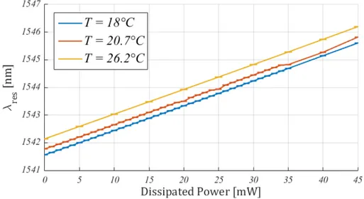
3.5 Chip Thermal Control . . . 109
3.5.1 Finer control . . . 111
3.6 Component Characterization . . . 114
3.6.1 Resistor . . . 114
3.6.2 Waveguide clips . . . 118
3.6.3 Variable Optical Attenuator(VOA) . . . 120
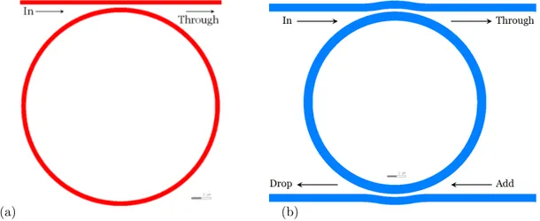
3.6.4 Add Drop Filter (ADF) . . . 121
3.6.5 IPC . . . 122
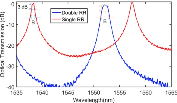
3.6.6 Interleaver . . . 126
3.7 BER performance . . . 127
3.7.1 Single node . . . 128
3.7.2 Add and Drop . . . 128
3.8 Second Version . . . 129 3.8.1 SPGC . . . 130 3.8.2 2DGC . . . 130 3.8.3 Polarization Controller . . . 132 3.8.4 Interleaver Characterization . . . 137 3.8.5 Double Ring . . . 138 3.9 Conclusions . . . 139 3.10 Future Perspectives . . . 140 Bibliography . . . 140 4 Polarization Controller 144 4.1 Introduction . . . 144 4.2 Device Schematic . . . 145 4.3 Single Wavelength . . . 145 4.3.1 Compensator . . . 145 4.3.2 Controller . . . 157 4.4 Frequency Response . . . 164 4.4.1 Compensator . . . 165 4.4.2 Controller . . . 169 4.5 Characterization . . . 171
4.6 Endless and Reset-Free Version . . . 173
4.7 Conclusions . . . 174
Appendix A SOI Effective and Group Indexes . . . 174
Appendix B MZI as an HWP . . . 175 Bibliography . . . 176 5 IRIS 178 5.1 Use case . . . 178 5.1.1 Network Delayering . . . 178 5.2 System Architecture . . . 179 5.2.1 IRIS Project . . . 182
5.2.2 Features . . . 183 5.3 Components . . . 187 5.3.1 Waveguide Crossings . . . 187 5.3.2 Interleaver . . . 187 5.3.3 AWG . . . 188 5.3.4 Switch . . . 189 5.3.5 Power Monitor . . . 191 5.4 BER test . . . 192 5.4.1 Single-Channel Test . . . 193 5.4.2 Interferometric Crosstalk . . . 193 5.4.3 Inter-Channel Crosstalk . . . 196
5.5 Mach Zehnder based De/Multiplexer . . . 197
5.5.1 Phase Noise Analysis . . . 199
5.5.2 System Characterization . . . 200 5.6 Conclusions . . . 205 5.7 Future Perspectives . . . 205 Bibliography . . . 206 Conclusions 209 List of Publications 211
Introduction
The two main pillars that underpin the Information Age in which we have been living for decades are digital electronics and optical telecommunications. Both managed to support and foster a prolonged exponential growth of hardware complexity and data transmission rates.
Thanks to integration first and CMOS technology then, electronics succeeded in keep-ing Moore’s law, statkeep-ing that the number of transistors on a chip doubles every 18 months, valid up to now, despite a slowdown in the last two decades as we are reaching the ultimate physical limits of silicon. About 95% of the overall semiconductor industry, and essentially all digital electronics, is based on silicon. The several virtues of this material enable mass and reproducible production of inexpensive and ever smaller integrated circuits with ever increasing features and computational power. This has led to the pervasive presence of electronic devices, and, in turn, of information technology, in many aspects of our daily lives and in industrial sectors not closely related to electronics. Consumer electronics is just the most immediate and clear instance of this process, but much more electronics is present in many applications without us even realizing of its very existence.
Similarly, optical telecommunications have been effective in providing an inexpensive and scalable medium and technology for long distance data transmission, where, since the mid 1970s, they have been steadily replacing coaxial and in general metal cables over ever shorter links. A major difference with electronics is that conventional optical telecommunications feature a rather small number of very expensive and quite big systems comprised of discrete high-performance components, each one optimized and using the best suited material to carry out its specific role, with no prevailing material, nor a standard technology.
The commercialization of the Internet at the turn of the millennium and the launch, a decade ago, of mobile handheld devices have been the main factors in keeping high the demand for more data traffic and in keeping a steady growth of data rates and network capacity.
The many Internet and cloud applications are supported by Data Centres (DC), each with the size of a big factory and hosting hundred thousand servers. Those facilities have to handle a huge amount of traffic and networking is becoming a bottleneck limiting their growth and scalability. The standard technology is 100 Gb Ethernet and 400 Gb Ethernet has recently been launched on the market. Electronic switching technologies are becoming ever less practical, both for their power consumption and bandwidth limitations deriving from losses and other impairments in metal interconnections, from parasite capacitances and from the unremarkable mobility of carriers in Si. Chip overheating deriving from the extremely high transistor density is another issue. Those factors brought to the stop of clock frequency scaling in microprocessors around the year 2000 and to the shift to multi-core architectures. On the contrary, photonic devices and optical interconnects have no practical speed limitations and can deliver bandwidths and throughputs in excess of THz. Nevertheless, legacy optical systems based on discrete (and sometimes free-space optics) components are not suitable to the DC environment neither to some network segments like Radio Access Networks (RAN) for mobile traffic, that would greatly benefit from the features, in particular reconfigurability, afforded by optical technologies.
Photonic Integrated Circuits (PIC) offer low cost and small footprint solutions to meet the aforementioned needs, together with the possibility of close integration with electronic circuits at the board and package level, and maybe, in future, on the same chip. In this way, electronic and photonics will complement each other. Optical interconnects are al-ready the standard in the longest links within DCs and in recent years they have been gradually superseding electrical cables of ever shorter reach. Anyhow, in the foreseeable future functions like data processing and storage will remain in the electronic domain. Indium Phosphide (InP) is today a mature platform capable of a moderately high scale of integration (some hundreds of components), offering a complete set of components, foremost high-quality lasers, amplifiers, modulators and detectors, together with passive elements like filters. However, it suffers from a high cost, and its yield, miniaturization and chip size are limited by intrinsic issues of the material and of the involved fabrication technology. It does not lend itself to mass production because of the lack of a production infrastructure and industry roadmap not even remotely comparable to silicon ones. Con-sequently, InP is well suited for integrating many transmitter or receiver units on the same chip, where its ability to efficiently emit, amplify, modulate and detect light is crucial, but it is not reasonable to use it to implement a large number of passive elements with a high integration density.
On the contrary, Silicon photonics can deliver large volumes of small size, inexpensive PICs with a large scale of integration, by leveraging the mature CMOS technology and its developed production infrastructure. It encompasses not just Si, but also Si compat-ible material platforms like Silicon Nitride (SiN). A roadmap for closer collaboration of research and industry has been published to provide access to cleanroom facilities even to entities than cannot afford them, by offering Multi-Project Wafer (MPW) services. Despite the lack of important components like lasers or amplifiers, the integration of SiGe photodiodes and the improvement of modulator technology represent important break-throughs already provided by the several foundries since several years by now. Solutions to equip Si photonic PICs with devices capable of emitting light are an intense research topic. Hybrid integration with III-V semiconductors is a rather compelling option. For all the above reasons, silicon photonics is the most likely candidate to meet the require-ments of datacom and some telecom segrequire-ments. Indeed, commercialization of Si photonics systems has already started in recent years.
1
Thesis Outline
The work of this thesis regards the characterization and modelling of silicon photonic switching systems for telecom and datacom applications. The thesis is structured in five chapters, the first two of which are introductory, while the other three describe the activities and the results undertaken during the thesis.
Chapter 1 is divided into two main parts. The first one describes optical telecommuni-cations starting from their historical development and introducing the several technologies, components, techniques, modulation formats, the network segments into which they are organized and the trends and criteria guiding their recent evolution.
The second part introduces the Data Centres (DC) landscape, beginning again from a historical perspective until the current cloud services. The several requirements that a DC is demanded to meet are listed and explained. The trends of this environment are then described. Albeit not immediately related to the topic of our direct interest, they are connected to optical networking in that some of them are aimed at the same goals of reducing power consumption and improving connectivity within the DC. Conversely, other trends as disaggregation would greatly benefit from optical networking because of the need to communicate with components placed further apart with the same performances of intra-server transmissions.
Chapter 2 introduces Silicon Photonics at a rather detailed level. Initially, a definition is given of what photonics is and it is compared to electronics. Then, the SOI technology is presented and a comparison is made with other material platforms used for photonic devices and systems, including the shortcomings of the current Si photonic technology. Drives and potential markets for Si photonics are pinpointed. Finally, a bottom-up de-scription is given, in order of increasing complexity, of the several structures, components and systems used in silicon photonics.
In chapter 3 the work carried out within the miniROADM project is reported. The project, in collaboration with Ericsson, regards the realization of a Si photonic integrated and reconfigurable switching system on chip, developed for deployment in Radio Access Networks (RAN), in view of the 5G launch. After describing the application scenario, an overview is provided of the evolution of cellular networks, with a particular emphasis on the base station architecture.
The C-RAN architecture is then illustrated, focusing on the fronthaul segment and on the requirements it imposes on the underlying optical transport and on the optical systems in it. The architecture proposed by the miniROADM is expounded, both at the network, node and chip levels, including protection mechanisms and the integrated components of which the chip is comprised.
It reports the several activities performed, like the characterization of the several building blocks, notably the Integrated Polarization Control, and the system level tests like BER measurements.
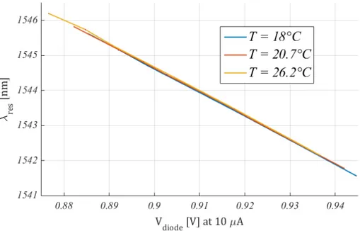
A temporary thermal control scheme was implemented, using the integrated SiGe photodi-odes as temperature sensors for feedback to the Thermo Electric Cooler (TEC) controller. As an optional study, it was evaluated the use of an integrated Si diode placed inside a microring resonator as a thermometer, to evaluate the resonant wavelength. It was used in a basic, not further optimized, feedback circuit.
Lastly, the components on the evaluation chips of the second miniROADM version were characterized. While inspecting the IPC building block, some predictions were tested of an analytical model developed to describe the operation of this device.
Chapter 4 presents the derivation of an analytical model of the polarization controller block. The analysis starts from the behaviour at a fixed wavelength, showing that, for any input State of Polarization (SOP), all the power coupled to the device input can be sent to the desired one its two output ports. Two classes of periodic solutions exist for every SOP. Conversely, it is proven that any SOP can be generated when the device is used in the opposite direction.
It is studied how the output power changes as a function of the two phase shifts. The properties of the resulting surface are listed, pointing out how they depend on the corre-sponding input SOP.
It was proven that the solutions are unambiguous, i.e. there are no two SOPs such that the first class of solutions of one SOP equal the second class solutions of the other. Hence, the IPC can be used as a polarimeter. A criterion is explained to find, without resorting to a trial and error approach, a phase shift pair that achieves polarization compensation. The second part examines the frequency response, which is found to be non-periodic, in general. An implicit equation is derived for the 3 dB bandwidth; from its first order ex-pansion, the effect of some forms of unbalance is found. Also, the reciprocal counterpart was considered, finding the curves traced on Poincar´e sphere, upon a wavelength change, by the point corresponding to the SOP produced by the system.
Finally, based on a solution found in literature, a schematic is presented to implement an endless version of the device.
Chapter 5 presents the IRIS project as a whole and in particular the different com-ponents. The last section reports the characterization work of a demultiplexer based on a binary tree of Mach Zehnder Interferometers (MZI) and the phase noise analysis of the
different MZIs designs, performed on batches of nominally identical devices. Four different prototypes based on three different MZI designs where evaluated. The initial part of the chapter presents the IRIS project to convey the framework of this activity.
2
Author Contribution
The candidate contributed to the experimental parts of both projects.
Regarding the miniROADM project, the author collaborated in many aspects of the project and in particular in setting up the TEC controller system using photodiodes as sensors, studied the feasibility of an enhanced thermal stabilization scheme using the Si diode integrated close to the microring to be tuned, in order to provide a more accurate temperature reading.
He performed electrical and optical characterization of the several components on both versions of the chip and participated in system-level testing, i.e. BER curve measurement, of the first version.
Finally, he developed an analytical model of the IPC module.
Within the IRIS project, the main contribution of the student was to characterize the Mach Zehnder based Mux and to perform the associated data analysis.
Chapter 1
Telecommunications
This chapter is intended as a brief introduction on several aspects of what will be mentioned in the following chapters.
1.1
Optical Networks
1.1.1 History
Before the invention, development and vast scale deployment of optical fibres in the ’80s, telecommunications used electrical wires for data transmission. Coaxial cables with atten-uation in the range of 20 dB/km were used for long haul lines. These high losses forced to place signal regenerators, that are complex and expensive equipment, every km or so, with consequent high capital expenditure (CapEx). At those time, the most likely succes-sor was thought to be wireless microwave antenna relays, that offered a larger capacity, together with easier and faster installation.
Optical Fibres
Ordinary glass has attenuation in the order of 103 dB/km. Charles Kao and George Hockam had the intuition that this is not a limitation of the material itself, but is rather due to impurities [1]. Following their 1966 paper, much research was directed at reducing
Figure 1.1: Absorption spec-trum of a conventional opti-cal fibre, with curves show-ing lower bounds for the sev-eral mechanisms producing losses.
contaminant concentration and at the start of the ’70s optical fibres with losses comparable to coaxial cables were developed. At the end of the ’70s, the attenuation was lowered down to its current value of 0.2 dB/km [2], close to the theoretical lower bound represented by
Rayleigh scattering. Standard single-mode fibres had three absorption minima at 850 nm, 1.3 and 1.55µm, called first, second and third window respectively (fig. 1.1). The last is the one with the lowest absorption, while the second has the smallest chromatic dispersion. Current, dry fibres have a single broad window from 1,3 to 1.65µm (fig. 1.2).
Figure 1.2: The three opti-cal fibre transparency win-dows and associated bands, together with the evolution of the absorption spectrum.
Semiconductor sources
In the meantime, GaAs semiconductor lasers were also invented and improved, as well as semiconductor photodetectors. Early lasers were based on homojunctions, i.e. junctions between two (or more) differently doped regions of the same material. This technology had the serious handicap of needing very large (105 A/cm2 at room temperature) threshold current densities. The reason is that, to reach population inversion, the current density is proportional to the thickness of the active region to be inverted; in the case of homojunc-tion this thickness is in the order of diffusion length, that is a property of the material. The breakthrough was represented by double heterojunction laser diodes [3, 1.4], wherein the central active region is jointed on its two sides with semiconductors possessing a wider bandgap, in the dubbed straddling configuration. The result is an ideally rectangular potential well in both the conduction and valence bands, so that carriers are confined in the central region with narrower bandgap.
The thickness of this region can be controlled with good precision (at the atomic level), and made significantly thinner than in homojunction lasers. This has allowed reducing the threshold current density by several orders of magnitude, together with other advance-ments, like quantum wells.
An added benefit is that the central active region has a higher refractive index (that tends to decrease with the bandgap), which also provides optical confinement of the optical mode in the vertical direction, so that light is concentrated in the gain region. However, due to the small thickness of the gain region (tens of nm), this effect would be negligible. Thus, a Separate Confinement Heterostructure(SCH) [3, p. 12] is used, that is, the thin active region is surrounded, above and beneath, by a material with an intermediate bandgap, thick enough to confine the electromagnetic mode.
Nonetheless, the major reason for switching from electrical to optical cables was not the attenuation, but the bandwidth. In fact, as explained in [4, pp. 121-167], metals performance degrades at higher frequencies: skin effect increases the series resistance by
reducing the effective conductor thickness, resulting in greater RC constant and attenua-tion. Moreover, capacitive losses become increasingly relevant with higher data rates. On the contrary, dielectric waveguides as optical fibres have bandwidths of hundreds THz, three orders of magnitude larger than the highest transmitted bit rates in coaxial cables, removing any practical limit; a further advantage is wavelength multiplexing, explained later on.
First Generation
The first generation of optical transmission systems was deployed during the second half of the ’70s. It relied on Multi-Mode Fibres (MMF). The light sources were often LEDs, both cheaper and simpler than lasers, thus more convenient to use with MMFs, as they have a core diameter of 80-100µm and therefore do not require very collimated nor small sources. Data rates were of tens of Mbit/s and transmissions took place at wavelengths near 850 nm, due to availability of lasers at that wavelength. The corresponding attenuation of 3 dB/km required signal regenerators to be placed almost every 10 km, which anyhow was a tenfold improvement with respect to coaxial cables. Data transmission was based on On-Off Keying (OOK), in which the binary symbol ”1” is encoded by transmitting light during the assigned bit slot, and the ”0” when no light is emitted.
The main limitation was the low bandwidth-distance product of MMF, in the order of some Tbit/second· m, mainly deriving from Modal Dispersion. The several MMF guided modes propagate at different velocities, therefore an initial, well-defined pulse is received as several different pulses arriving at slightly different times, causing a smearing of the original pulse. Beyond a certain distance, decreasing with the bit rate, the broadened pulses invades the neighbouring bit periods by an excessive amount. The resulting Inter-Symbol Interference is too large to recover the information.
Second Generation
To overcome this limit, the second generation, which started operation in the mid ’80s, passed to single-mode fibres (SMF), marked by a smaller core diameter of 10µm. As they support only one guided mode, the issue described above, due to multi-modal dispersion, is removed.
Moreover, the transmissions were performed in the 1.3µm window, featuring a negligible dispersion.
This was allowed by the development of InP based lasers. Lasers allow a higher output power than LEDs, thus longer distance transmission. Moreover, they have a narrower spectrum.
Still, second-generation systems made use of Multi Longitudinal Mode (MLM) lasers, whose emission spectrum displays many peaks over several nm or even tens of nm. The longitudinal laser modes are not to be confused with the fibre modes, that are field distributions in the fibre transversal direction (sec. 2.2.1).
This derived from using a Fabry P´erot design; the frequency (or wavelength) spacing of the resonant longitudinal modes of this cavity type, called Free Spectral Range (FSR), is inversely proportional to its length (eq. 2.57).
In order to have a reasonably high output power, the laser cavity cannot be made so short to have a single resonant wavelength in the active material gain band.
All of those actions allowed to further increase the distance between consecutive repeaters to about 50 km. At this point, the limiting factor was again fibre loss, now reduced to 0.5-1 dB/km.
Third Generation
In the late ’80s, the third generation addressed this limit by moving to the 1.55µm window, where losses are the lowest. Notwithstanding that, therein chromatic dispersion is quite strong.
Chromatic dispersion is the dependence of light group velocity on its frequency. Group velocity is the speed at which the envelope of a wave, which is the one carrying information, propagates, as opposed to phase velocity. Its effect is to change the pulse width, generally increasing it, ultimately causing ISI. It derives both from material intrinsic dispersion and from the one introduced by the waveguide structure [5, 2.3].
This problem could be addressed by reducing either fibre dispersion or signal bandwidth. Both solutions were adopted, using dispersion-shifted fibres (DSF) [6, sec. 2.4.2] and/or Single Longitudinal Mode (SLM) lasers. Most operators opted for the second option, as they had already installed a network of SMF just some years before.
Moreover, the change of wavelength implied passing from InP to InGaAsP based lasers, more complex to produce in large scale. Another significant progress regarding lasers, as already mentioned, was to reduce their spectrum width by having a single peak. In traditional Fabry P´erot lasers, the feedback is given by the reflection at the lumped mirror at the cavity end facets. Their reflection spectrum is nearly flat. On the contrary, a Bragg mirror based on a grating can be designed to have a reflection peak at a certain wavelength and low sidelobes in the FSR between neighbouring peaks. In this way, a single longitudinal mode can be selected while the others are strongly suppressed. The most widespread approach is to incorporate the grating in the gain region, in what is called a Distributed FeedBack (DFB) laser [3, 3.6-7].
Coherent Receivers The inter-repeater distance grew to about 100 km. Further reduc-tion of fibre losses is not physically possible because of the limit represented by Rayleigh scattering.
One proposal was to increase the receiver sensitivity by using coherent detection schemes [7, Chap. 2]. The basic idea is to multiply the incoming signal by that of a local oscil-lator. In electronic systems, this is done either by exploiting non-linearities of diodes or transistors or by using specific circuits like Gilbert cell.
The first approach is also used in optics. Signal and LO are combined, and the non-linearity comes from the fact that a photodetector is sensitive to the power, that is, the square of the field impinging on it:
IP D = RP ∝ Es(t) ei(ωct+θs(t))+ ELOei(ωLOt+θn(t)) 2= = RhPs(t) + PLO+ 2 p PLO· Ps(t) cos (ωIFt + θs(t)− θn(t)) i ωIF =|ωs− ωLO| (1.1)
Where IP D is the photodetector current, ωcand ωLO are the signal carrier and local
oscil-lator angular frequency, respectively. The information is encoded in the signal amplitude Es(t) or on its phase θs(t), while θn(t) is the LO phase noise. The term ωIF indicates
the intermediate angular frequency resulting from the beating. Depending on its extent respect to the signal bandwidth B, three cases are possible:
• ωIF B Heterodyne scheme;
• ωIF > B Intradyne;
• ωIF = 0 Homodyne
The first two terms in eq. 1.1 can be cancelled out using a balanced receiver [7, 2.2]. The third term shows that the signal amplitude is multiplied by that of the LO laser, therefore
the result is signal amplification or, equivalently, an enhanced sensitivity [7, p. 13]. Added to this, also the signal phase θs(t), not just its amplitude Es(t) can be retrieved, so more
advanced modulation formats other than OOK can be used and they permit to increase the spectral efficiency.
However, optical coherent detection is not as straightforward as its radio equivalent, be-cause of many impairments arising from many factors [5, 10.5] [7, 2.1.1], mainly polariza-tion tracking and locking the LO phase to the transmitter’s one.
Fourth Generation
The commercialization of Erbium-Doped Fibre Amplifiers (EDFA) at the end of the ’80s changed the perspective and coherent systems lost most of their attractiveness. Essentially, an EDFA is a strand of fibre, whose core is doped with Er ions, and that, once optically pumped, amplifies the incoming light through stimulated emission. As pointed out in [6, 1.8.3], the idea of EDFA was conceived in the ’60s, but it became workable just when reliable high power pump lasers were available.
Optical amplification has several advantages over traditional regenerators. It is simpler and faster as it does not need EOE conversion. Then, it is insensitive to the particular data rate, modulation format and network protocol used by a particular channel. Together with a gain band tens of nm wide, all these aspects enable to amplify many channels at once with the same EDFA, that can replace the numerous regenerators previously used. On the other hand, like electronic amplifiers, EDFAs deteriorate the signal quality by adding noise. The most relevant source of noise is Amplified Spontaneous Emission (ASE) [5, 6.4.4]. Other kinds of amplifiers, like Raman [6, 3.4.4] or Semiconductor Optical Amplifiers (SOA) [5, 6.2-3], can be used to complement EDFAs.
WDM The most distinctive trait of the fourth generation was the adoption of Wave-length Division Multiplexing (WDM), that is, transmitting different data streams on the same transmission medium - the fibre - with carriers at different wavelengths, akin to what has been done for radio or television broadcast. The link capacity could now be increased in a scalable way: instead of the lengthy and costly R&D needed to increase the data rate of a single channel, the link capacity could now be raised by adding other channels and buying additional modules with the same bit rate. The same EDFAs could be left in place, whereas previously the line repeaters would have had to be upgraded.
For the third time, due to the longer inter-regenerator distances afforded by EDFAs, dispersion showed its detrimental influence. Two countermeasures were taken, namely external modulation and dispersion compensation.
Although laser bandwidth was narrowed thanks to SLM lasers, yet direct amplitude mod-ulation has the unpleasant side effect of causing a spurious frequency modmod-ulation known as chirping [3, 5.3.3,5.4.4]. The reason for that is the variation of the refractive index deriving from the higher charge carrier density connected with a higher current. To avoid this, the laser is biased with a constant current and a downstream modulator transfers the data on the carrier. This arrangement is called Externally Modulated Laser (EML). Also, new components as De/Multiplexers (De/Mux) appeared in optical network systems, in order to separate/combine the several WDM channels coming from/to be sent into an optical fibre.
This revolution of the optical networks coincided with the dot-com bubble in the second half of the ’90s until its collapse in 2001. The bubble fuelled a massive network expansion because of the data traffic growth provoked by commercial diffusion of the internet. Dispersion Compensation The second remedy was to compensate for the dispersion accumulated on a segment of SMF by having the light to propagate in a rather short span of dispersion compensated fibre. This type of fibre has an index profile engineered so as
to have a strong negative chromatic dispersion. The same approach was used with DSF to minimize dispersion for wavelengths around 1.55µm.
Non-linear effects Unfortunately, amplification provided by EDFAs meant that light channels could now stay above a minimum power (and thus intensity) level, consequently, non-linear effects came into play. The issue was exacerbated by the effort previously done to contrast chromatic dispersion, especially the installation of DSF, which proved counter-productive as the pulses from different WDM channels travelled at similar group velocities and thus interacted for long distances.
Indeed, among the host of different nonlinear effects that may appear in optical fibres, the most influential ones in terms of performance degradation are Self-Phase Modula-tion (SPM), Cross-Phase ModulaModula-tion (XPM) and Four-Wave Mixing (FWM) [6, 2.5.6-7] and can be made negligible with a moderate chromatic dispersion. The new Non-Zero Dispersion-Shifted Fibre (NZ DSF) was developed to have a dispersion of 2-4 ps/(nm km) against the 17 of traditional SMF; the reasons for that are the higher losses and non-linearities of DCF due to its smaller effective area. In this way, shorter spans of DCF are needed.
Fifth Generation
With the fifth generation, in the second half of the new millennium first decade, there was a comeback of coherent detection schemes after they had been neglected for nearly two decades. Coherent systems not only possess a greater receiver sensitivity but also allow a greater spectral efficiency, as more than one bit can be encoded in a given transmitted symbol. Spectral efficiency is defined as the ratio between the bit rate and the channel bandwidth:
SE = Rb
B (1.2)
For binary formats, this quantity is limited to about 0.8 bit/s/Hz, since usually a 40 Gbit/s WDM channel occupies an analogue bandwidth of 50 GHz. This figure can be enhanced by a factor N if N bits are encoded in each symbol.
Whereas this can also be done with Intensity Modulation and Direct Detection (IMDD) schemes using, for instance, Pulse Amplitude Modulation (PAM), still the possibility to recover the full complex signal afforded by coherent receivers is advantageous in terms either of noise immunity or of energy efficiency, together with the possibility to use more advanced modulation formats.
In fact, in the language of constellation diagrams as in fig. 1.3, in OOK and PAM formats the symbols are restricted to the positive real axis, while coherent systems can distinguish symbols placed anywhere on the IQ complex plane. As an example, comparing OOK with Binary Phase Shift Keying (B PSK), if the peak power is the same, then BPSK has twice the symbol distance, if instead the distance between the two symbols is maintained, it uses half the power. Consequently, constellations centred on the origin, which minimize the average energy per symbol while keeping a given bit error rate (BER), can be employed. Moreover, with coherent detection also the state of polarization (SOP) can be extracted, introducing another degree of freedom that can further increase spectral efficiency by a factor 2.
Nonetheless, it must be emphasized that spectral efficiency cannot be increased ad libi-tum. First, increasing the number of symbols of a modulation format (while keeping the maximum power constant) reduces the relative distance among them in the constellation diagram, thus complicating their discrimination because of the noise. Second, the Signal to Noise Ratio (SNR) cannot be raised at will, because of the degradation from non-linear effects arising with increased power. The theoretical limit to spectral efficiency is in the order of 9 [8].
I Q ’0’ ’1’
OOK
00 01 10 11PAM 4
I Q 1 0BPSK
I Q 00 01 10 11QPSK
I Q8 PSK
I QQAM
I Q16-QAM
Figure 1.3: Constellation diagrams for several modulation formats. The horizontal blue line divides single polarity formats like OOK and PAM from the ones requiring coherent detection, like PSK or QAM. In this case, OOK and PSK have the same peak power.
In essence, the several degrees of freedom that can be exploited with coherent systems were also the reason why this method was adopted later: IMDD is insensitive to the ran-dom phase and polarization fluctuations happening during propagation, and thus is more robust.
As a closing remark, a LO oscillator is not an indispensable element of coherent schemes. Indeed, in differential modulation formats (like DQPSK or DPSK), the signal itself can be used as reference [9, 5.3.1.3] [7, pag.16]. Clearly, this simplification comes at the cost of losing the amplification deriving from the LO; nonetheless, in situations where the signal power is not too low (or can be amplified with EDFAs without particular drawbacks) this is not a major concern. Another advantage of coherent communications resides in the fact that WDM filters can be removed therefore simplifying the network.
DSP Anyhow, what determined the success of coherent detectors was the progress in Digital Signal Processing (DSP) electronics.
The basic idea behind DSP is that of processing a signal (or an image) in the digital do-main, rather than with analogue systems [10]. The input signal is sampled and discretized with Analogue-to-Digital Converters (ADC), then processed either in the (discrete) time domain with Finite or Infinite Impulse Response (FIR/IIR) filters, or in the frequency domain by means of Fast Fourier Transform (FFT) or other techniques.
to signal quantization, ability to implement time-varying or adaptive filters, and above all, being programmable by software, thus not requiring a hardware change in response to an algorithm upgrade. Last but not least, signal quantization inherent to digital sys-tems grants them nearly perfect reproducibility, whereas analogue devices suffer from the dispersion of parameters values with respect to the design ones. The same is true for information storing, that on analogue supports gets altered each time it is copied.
The availability of high-speed Digital Signal Processors used for radio communications enabled to circumvent the many stability issues that challenged a reliable synchronous detector.
Beyond the need to track the input SOP (that can be solved by splitting the two po-larizations and processing them with two separate identical circuits, in what is called Polarization Diversity, [7, 2.2.4]), the main problem for obtaining an optical equivalent of Phase-Locked Loops (PLL) regularly used in many electronics applications is that com-mon semiconductor lasers have a noise bandwidth of the MHz order. This mandates for a very short loop delay for obtaining stable and reliable locking, and is not so simple to meet this requirement.
Thanks to DSP circuits, the carrier phase could now be detected in a precise way. Also, the several impairments arising from propagation, like chromatic and polarization mode dispersion, or non-linear effects, can be compensated by software [7, 2.3]. Furthermore, Forward Error Correction (FEC) algorithms can be applied [11, Chap. 8], as well as clock recovery [9, Chap. 14].
Evolution towards All-Optical Networks
The five generations described up to now, more than to networks, refer to point-to-point links and the technologies used in their physical level implementation. In this sense, they are indicated as a whole by ”first generation”, from an architectural standpoint. In con-trast, second-generation optical networks also possess features like routing, switching and management functions, that are performed in the optical domain.
Previously those functions were carried out by electronic components, thus requiring OEO conversion. This approach becomes more burdensome with increasing bit rate since elec-tronics have less time to process the same amount of information, together with the other issues considered in sec. 2.1.6. Considering that most of the data streams just transit through a node, doing networking at the optical level is not just conceptually simpler, but also allows relieving the burden on the electronic equipment, since now it is required to process just the traffic intended for that node. The use of optical networking facilitates operation, as optical systems are transparent - within certain bounds - to modulation for-mats, network protocols and allow for broader bandwidths [6, sec. 1.5, 5.12.9]; in principle, they allow transmitting analogue signals, not just digital ones, which is exploited in access networks (e.g. for broadcasting analogue videos). Other advantages are the cost reduction deriving from lifting the need of OEO conversion [12, sec. 2.5].
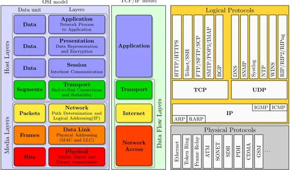
With the second generation of optical networks, the optical layer was introduced [12, sec. 1.3] [6, sec. 1.4]. They are termed ”All-Optical Networks”, though there could be some disagreement regarding the ”all” [12, sec. 2.5]. Its role is to provide lightpaths to the higher layers of the network stack (TCP, or ISO/OSI, illustrated in fig. 1.4 [13, sec. 1.5.1]). A lightpath is a connection between the end-users passing across several intermediate nodes, along which the information remains in the optical domain, at the assigned wave-length (which however can be changed along the path, if necessary, with wavewave-length con-verters [6, sec. 3.8]). The provisioning of lightpaths involves design stages distinct from that of the physical link [6, Chap. 10].
A prerequisite for All-Optical Networks is WDM since light paths sharing the same links must travel on distinct wavelengths. The three key enabling network elements are
OSI model TCP/IP model Bits Frames Packets Segments Data Data Data Data unit Physical
Media, Signal and Binary transmission
Data Link
Physical Addressing (MAC and LLC)
Network
Path Determination and Logical Addressing(IP) Transport End-to-End Connections and Reliability Session Interhost Communication Presentation Data Representation and Encryption Application Network Process to Application Layers Media La yers Host La yers Application Transport Internet Network Access Data Flo w La yers Physical Protocols Ethernet T ok en Ring F rame Rela y A TM SONET SDH PDH CDMA GSM · · · Logical Protocols IP ARP RARP ICMP IGMP TCP UDP
HTTP/HTTPS Telnet/SSH FTP/SFTP/SCP SMTP/POP3/IMAPSMTP/POP3/IMAP BGP DNS SNMP Systlog NTP WINS RIP/RIP2/RIPng
Figure 1.4: Protocol stack for the OSI (left) and TCP/IP (centre) models. The block on the right list the several protocols in actual implementations.
and transmit/receive the data streams. Their essential components are transceivers and De/Mux. An important remark to avoid misunderstandings is that OLTs are not necessarily the watershed between optical and electronic domain signals, but rather between the optical layer to higher layers: indeed they are usually connected to client equipment like IP routers with SMFs. However, the communications may occur in the 1.3µm window, so transponders are needed for converting wavelength to 1.55µm.
• Optical Add-Drop Multiplexers (OADM) [6, sec. 7.3] can add or drop channels while letting the other wavelengths just transit the node, without O-E-O conversion. The reduction of the transponders count allows lowering the cost and power consumption of each node. Usually, OADMs are placed in nodes inside a ring topology, possessing a degree 2, meaning that two links pass by every node. Nonetheless, multi-degree OADMs are not uncommon; often they are placed at the junction between two ring networks.
• Optical Cross Connects (OXC) [6, sec. 7.4] can handle more complex topologies, like mesh ones, and have a larger port count than OADMs. They are usually placed in network hubs, like carriers central offices, whereas OADMs are located along a link or at the boundary between two network rings.
Those are the optical analogues of their SONET counterparts [6, sec. 6.1.6]. A limitation to a truly all-optical network is multi-vendor interoperability [6, sec. 8.4], which is why usually the channels undergo OEO conversion when passing from the system by a vendor to another one.
Another useful component is the wavelength converter [6, sec. 3.8], which often is implemented simply by interfacing two transponders, one used as the receiver and the other to transmit on the new wavelength. Wavelength conversion enhances network flexibility by adding another degree of freedom. It may happen that a wavelength is free just on part of the path between two endpoints while another wavelength is available on the remaining section. With the constraint of wavelength continuity, the two ends cannot be connected. Wavelength conversion lifts this limitation.
As a final remark, the optical layer makes use of circuit switching, in contrast to higher layers like IP or Ethernet that are based on packet switching. While Optical Packet Switching (OPS) [6, Chap. 12] would allow a more efficient bandwidth utilization, it has remained at the research stage, mostly due to the lack of a practical Random Access Memory (RAM) in the optical domain. Similar considerations hold for Optical Burst Switching (OBS) [14, Chap. 18] as well.
Dynamic Networks
In second-generation networks, the wavelength assignment was static, meaning that changes in wavelength provisioning or routing happened on scales of months or years. The princi-pal reason was that network elements were not reconfigurable: each port was assigned to a specific wavelength and direction, so any update of those parameters required manual intervention for moving cables, transmitters or receivers to the proper new ports. Planning network rearrangements was lengthy and cumbersome, in that technicians had to carefully plan the overhaul [6, sec.8.6.2, 7.3.1] [12, sec.8.1].
The current (from mid-2000s) paradigm is to dynamically reconfigure the network connections on time scales that can be as short as minutes, for a better resource utilization, to avoid the congestion of some links and to follow traffic patterns, among the many drivers [12, sec.8.2]. Clearly, the traditional approach is not viable. For these reasons current network equipment is remotely reconfigurable by software, using concepts like ASON (Automatically Switched Optical Network) [6, sec.8.6.2] or SDN (Software Defined Networking) [12, sec.8.11] [13, sec.5.5].
The distinctive network element of this generation is the Reconfigurable OADM (ROADM) [6, sec 7.3.2] [12, sec.2.6-10]. Traditional ROADM implementations are based on free-space optics solutions. The switching engine is based on MEMS actuated mi-cromirrors [15, Chap. 6] or arrays of liquid crystal cells [15, Chap. 5] [16, sec. 11.4].
Equipment based on those technologies is quite expensive and bulky, so it is cost-effective just in the core and metro segments. Photonic Integrated Circuits (PIC), es-pecially silicon photonic ones, can significantly reduce both cost and footprint, together with a potential for mass production that is difficult to achieve with legacy discrete im-plementations. These three elements may favour the deployment of reconfigurable optical equipment in the access segment of optical networks. For the reader interested in more details, the white paper offered by Huawei ”White Paper on Technological Developments of Optical Networks” offers many interesting developments on the trends of the optical networks.
1.1.2 Network Segments
Optical networks are not a single, uniform entity, but (for reasons partially explained in [13, sec. 1.3.3]) are rather grouped into three main segments, which can be labelled with equivalent names, based mainly on their geographic extent and capacity:
• core, backbone or long haul networks [6, sec. 13.2.5], spanning from several hundred to more than ten thousand km, depending on the location (European links are significantly shorter than North American ones, while transoceanic cables can exceed the length of ten thousand km). Needing a large capacity in the order of several tens Tbit/s, they usually exploit the most advanced technologies such as Dense WDM (80 wavelengths in the C band spaced by 50 GHz, as specified by ITU-T G.694.1), bit rates of 100 Gbit/s (OC 1920) or more, advanced modulation formats like 16 QAM and optical networking elements like ROADMs.
They adopt a mesh topology or a mesh of interconnected rings when the node density is low, as in North America. The reason is that data traffic is mainly meshed [6, p. 711] and rings are not the most efficient choice to accommodate such traffic [6,
sec. 9.5.8]. Also, meshes have a higher level of redundancy and thus require less spare capacity for protection [12, sec. 7.4.2].
• metro networks [6, sec. 13.2.8], which in turn are distinguished in 2 sub-segments: – metro access/aggregation: its role is to aggregate the traffic from the access
network, concentrating it into the carrier’s central office or distributing it in the reverse direction. It extends on distances of some or a few tens of km. – metro interoffice/regional: it connects the central offices inside a metropolitan
area or region, usually separated by distances in the range of several tens to hundred km.
The bandwidth is not as big as in the core segment, but anyhow DWDM and coherent detection have been widely deployed. Beyond the traffic growth, another factor favouring WDM over TDM or SDM (Time and Space Division Multiplexing) are the convenience for carriers to offer a wide service mix to the several different client types [6, chap. 6]. A big share of metro traffic is dedicated to interconnecting data centres located in the same area. The rapidly varying traffic distribution is a major reason that has driven the fielding of all-optical switching elements.
Typically, a ring topology is used because of its simplicity while still providing a good degree of survivability [12, sec. 7.4.1] [6, sec. 10.1], but mesh topologies - to a different degree - might be implemented as well.
• access networks [6, chap. 11] cover the last few km from the carrier central office to the subscribers’ location. They rely on several different media, ranging from copper twisted pairs, coaxial cables, optical fibres or wireless. Usually, they adopt a star or tree topology. Optical fibre access network are termed Fibre to the x (FTTx) [6, 11.3], depending on the distance between the fibre end and the final user. As this segment serves tens to few hundreds of subscribers, its cost is critical in determining the final subscription price. This dictates that the network must be as simple, reliable, low cost, easy to maintain and operate as possible. Hence the most popular choice are1 Passive Optical Networks (PON), meaning that no network elements that need to be powered/controlled (like ROADMs) are deployed, but rather passive ones like splitters or AWGs. Some architectures support WDM. The above classification refers to public networks, that must not be confused with private networks. Those are distinguished, following similar criteria, into Local, Metro and Wide Area Networks, abbreviated in LAN, MAN and WAN, respectively.
The several network topologies that have been mentioned are illustrated in fig. 1.5.
1.1.3 Trends and rationale
Installing a fibre optic link costs some tens of thousand dollars per km, a tenth of which only is represented by the cost of fibres. Thus, the general approach is to devise solutions that allow upgrading the network while maintaining the existing infrastructure, limiting the changes to the installed equipment. For the same reason, many more fibres than currently needed are laid down when building a new link; the unlit ones are referred to as ”dark fibres”. Solutions that allow to smoothly upgrade the system without needing major overhauls are said future proof. For example, the transparency to bit rates (up to an upper bound), modulation formats and network protocols protects the infrastructure against changes, besides providing flexibility.
Another useful paradigm is the ”pay as you grow” one: solutions allowing to grad-ually expand the network as the traffic demand increases are to be preferred. Instances are the possibility to expand a link capacity afforded by WDM, by simply adding other channels on the same fibre.
Ring
Star
Bus
Full Mesh
Partial Mesh
Tree
Figure 1.5: Scheme of the several possible network topologies.
Optical communication systems are more suitable than electrical ones beyond a certain bandwidth-distance product threshold. Consequently, they have been installed starting from long haul and high-speed links and have gradually spread in other network segments down to the metro and access ones as the traffic grew.
The data rates tend to be larger for longer reach segments; nonetheless, to efficiently exploit a 10 or 40 Gbit/s rate, several lower rate data streams have to be time-multiplexed on the same wavelength. If some of the streams have to be dropped/added at a node along the journey, than OEO conversion is needed (the process of adding/dropping TDM streams and rearranging them is termed grooming [12, Chap. 6]), so - depending on the scenario - it could be more practical to opt for more lower rate wavelengths carrying fewer streams.
The same pattern applies to the deployment of technologies such as WDM, coherent systems or network elements.
Several factors point in this direction. Segments spanning longer distances need greater capacity and longer reach. Covering a wider area, they serve a larger number of users among which the overall cost is shared. Instead, segments closer to the final user are less demanding in terms of performance, but, being shared among fewer customers, they have a major impact on the final subscription price.
Also, different business models apply to the different segments [14, sec. 1.3].
In the end, the metric telling whether upgrading to a new technology is economically favourable is the cost of the transmitted bit per km. Usually, carriers seek to quadruple the capacity; this is cost-effective when the new equipment cost is about twice that of the current one [6, p. 718].
Other considerations are whether a capital cost can reduce the operational costs or if the upgrade affords to provide new services, meaning more revenue. For instance, optical switching permits to reduce the redundant fibre links reserved to protection or to use them even during normal conditions [12, ch.7].
1.1.4 Requirements
Different network segments have different needs. For long haul networks, it is worth to opt for advanced, costly, power-hungry, bulky and maintenance demanding equipment that provides high performance. On the contrary, in access networks the focus is more on containing costs, so inexpensive, passive or low power components are preferred.
Another element is production volume: the closer a segment is to the subscriber, the larger is the number of units to be deployed; whereas, longer range segments require few elements, so production volume and unit cost are not critical.
Interoperability among equipment from different vendors is a desirable feature for the carriers, but not so straightforward to implement [6, sec. 8.4].
1.2
Datacom
By itself, the term ”Data Centre” (DC) may designate any computation cluster whose size varies from few servers inside a cabinet to hundred of thousands of servers spread over several interconnected buildings in the same metropolitan area.
Originally [17, ch.1], data centres were privately owned and operated by businesses (or organizations such as universities) to process their data with a mainframe computer and store them.
In the 1960-70s it was widespread practice to have several terminals time sharing a cen-tralized mainframe computer, following the client-server model. Terminals were used for entering inputs into and displaying or recovering results from the computing system that processed the data. This gave the users the impression of having exclusive control of a lower performance computer, as if it were located in their terminal. The expression ”data centre” originated in that context, referring to the rooms designated to house computing systems.
With the advent of mini and personal computers in the 1980s, this approach lost popu-larity.
The commercialization of the Internet in the 1990s led to data centres in the current acceptation and to a resurgence of the client-server model, for manifold reasons.
The most immediate one is that web pages are stored in web servers, which take care of distributing those contents to clients that require them upon a web search. As those contents should ideally be always available, servers should always be on (actually, a server/application crash is not an uncommon event, but often it is rather innocuous, as long as other servers can perform the crashed server’s duty until its recover). Not every company, especially small ones, could afford their own data centre, so they rented those resources from an Internet Data Center (IDC) operated by a provider.
Other drivers were e-mail, e-commerce, instant messaging, home banking, video streaming and many more applications (in the sense of ISO/OSI layer 7 [13, sec.1.5.1]). As an ex-ample, in the case of web search, the client runs the web browser but the actual search is performed inside a remote data centre [13, sec.6.7], or, better, in the cloud; nonetheless, the whole process is so swift that the user has the impression that it is run locally on one’s own device.
As the big companies, whether they be content/service providers like Google and Microsoft, e-commerce players like Amazon, or others, have their own big data centres and even global networks [13, sec.2.6.3], it is convenient for them to rent a part of them to third parties. In this way, they can leverage economies of scale while their customers can reach significant savings with respect to the traditional option of privately owned and managed DCs. Small enterprises that otherwise could not have afforded their own facilities, equipment and personnel, can now have their activities, applications and more hosted in a provider’s DC. This approach allows them to concentrate on their core business, without needing an IT department, which is usually out of their expertise area. A similar argument holds for startup companies. Big companies already possessing their DCs may opt for leasing space instead of expanding their own (hybrid cloud [18, sec.1.2.2]).
The services provided can range from resources [18, sec.1.2.2.3], like computing or storage, to platforms [18, sec.1.2.2.2] or applications [18, sec.1.2.2.1]. The latter case can be seen as a comeback to the mainframe-terminal architecture, but on much greater distances.
Several services models are possible [18, ch.3], namely the ”as a service”, ”on demand” or ”pay per use”.
1.2.1 Requirements
Availability
Almost all services provided by companies or institutions through the Internet should be always available; this translates into a similar requirement for DCs that host those appli-cations [19, ch.35]. A standard by the Uptime Institute [20, sec.1.3] classifies data centres in 4 tiers with increasing availability, or shorter downtime along a year’s period.
High availability is achieved by redundancy, uninterruptible power sources (UPS), power generators and non-disruptive replacement of broken parts. Reliability, modularity asso-ciated with physical or logical separation to confine failures, simplicity of design, avoiding Single Points of Failure (SPoF) and automatic recovery are further ways to enhance avail-ability.
Disaster Recovery
The possibility that a natural or man-made disaster damages a data centre or anyway blocks its operation for a substantial time span must be considered and proper recovery plans devised [19, ch.35,36]. In order to reduce the risk of natural disasters, data centres are preferentially placed in zones not prone to earthquakes, hurricanes, floods or other calamities.
Security
Many applications, whether cloud ones or not, hosted in data centres can be quite sensible. Consequently, security [21, ch.4], both at the physical and software level, is a crucial element, to protect data, hardware and software from attacks. The matter is further complicated by multi-tenancy, because applications used by different customers share the same physical resources but must be kept logically separated.
Data Preservation
Data centres must include backup, recovery and restoration plans for avoiding data loss or inaccessibility deriving from failures, disasters or cyber-attacks [21, ch.5]. Backup copies may be located in sites very distant from the original one.
Scalability
An entity is said to be scalable if it is able to maintain a set of properties upon a size change. In the case of data centre networks, the scale is usually expressed in terms of the number of interfaces, but other metrics may be considered.
As the sector is steadily expanding, preferred solutions are those that keep the port unit cost, latency, power consumption and complexity reasonably low while achieving good performance and reliability.
The dynamic nature of many cloud applications also requires dynamic scalability, i.e. that the resources assigned to a given application can be rapidly expanded or reduced to accommodate traffic and demand spikes. This is mainly addressed with virtualization. Power Consumption
A current mega data centre consumes several tens MW and DCs as a whole consume more electricity than the UK. New DCs are built in locations with a cold climate, to facilitate
cooling, and close to power stations, preferably from renewable sources [22, Ch. 1,2]. The energy efficiency is measured by means of the power usage effectiveness, defined as the ratio between the total power absorbed by the facility and that consumed by IT equipment:
P U E = PT ot PIT
(1.3) The goal is to make this quantity as close to 1 as possible. The major factor that deteri-orates (increases) PUE is cooling, which takes from 1/3 to half of the total power [23]. In this regard, one countermeasure is to adopt passive cooling systems and to keep the data centre environment at a hotter temperature; the drawback is a lower equipment density and a greater inter-device distance [24, p. 406], which in turn impacts networking gear requirements in terms of link distance and capacity.
Virtualization, by improving resources utilization, has contributed to improve energy effi-ciency, as well as remote management: some big data centres, especially those located in remote places, work in ”lights out” mode, with almost no staff stationed in the facility, thus cutting on the associated utilities.
In many areas, notably in the electric grid and other systems handling large amounts of power, the primary driver for energy efficiency, more than energy or cost saving, is to limit the strain on components: if an element is traversed by several MW, even a slight deviation from close to 100% efficiency results in several kW being dissipated. A costly and bulky cooling system would be needed to prevent performance degradation or permanent damage. At the opposite end of mobile or low power devices, the leading motivation is to extend battery autonomy.
In the case of data centres, nonetheless, even the sheer cost of electricity takes its toll, in that an average power of 1 MW corresponds to 1 million $ spending per year (up to a factor of few unities, depending on local electricity pricing).
The requirement of conserving the existing infrastructure, like racks, power supply and cooling systems, puts an upper bound on the power drained by devices housed in the same rack. In the end, this consideration amounts to a maximum dissipated energy for processed/transmitted bit metric, typically in the order of p-fJ/bit [20, sec. 1.9]. Given that the prerequisite for transitioning to a new equipment generation is a two or fourfold speed growth, the above figure should decrease by the same factor.
It is one of the most important factors, for what concerns this work, as photonics can attain high data rates and long reach together with low power consumption, whereas electrical cables cannot.
1.2.2 Current Trends
Virtualization
Virtualization is a widely used procedure in computing. The basic idea is to give any entity using the computing system (a process, thread, user or whatever) the impression of having the exclusive control of a virtual version of a resource (CPU, memory, storage, peripherals, machine and more). It is closely related to the already introduced concept of time-sharing.
It has the twofold advantage of allowing multiple processes to use ”simultaneously” the same physical machine and of achieving more efficient resources utilization. Indeed, pro-cesses often do not use system resources uniformly in time, but rather tend to alternate long idle periods to short and intense active ones. If each process were to have its own ded-icated resources, dimensioned to fulfil worst-case requirements, then most of them would be wasted and both CapEx and OpEx would be unreasonably high respect to an equivalent virtualized counterpart. Instead, the operating system (OS) provides each process with a tailored amount (that can even change dynamically) of the requested resource. Doing
so in hardware would be troublesome both because of large granularity (few options are possible for CPU, RAM, disk capacity/speed, generally scaling in powers of 2) and the impossibility of dynamic adjustments.
While virtualization is an established practice in the area of operating systems [25, ch.3-13], its scope is not limited to it. In the data centres context [26], the main actions are virtualizing
• servers • storage • network
Moreover, one may say that the data centre itself can be virtualized [22, ch. 3], both because the trend is (as will be discussed) to spread it over several facilities that can be quite far apart and because some tenants perceive to operate their own (virtual) DC.
Storage virtualization consists of presenting pooled (and generally heterogeneous) stor-age devices as a single virtual device [27, ch.3]. While many aspects are not that different from what is traditionally done by OSs [25, ch.10-13], there are security concerns [18, ch.13,14]. The Storage Area Networks (SAN [6, sec.6.8]) interconnecting storage devices do not tolerate dropped nor out of order packets.
Servers are virtualized by having them host multiple virtual machines (VM) [25, ch.16]. This enhances server utilization, thus reducing the number of physical servers required to meet a given demand, translating in a lower footprint and power consumption [21, ch.10]. It boosts security as well, in that applications that are to be kept separated are run on distinct VMs, potentially with different OSs. Further advantages are faster provisioning (a new VM is created instead of starting a server), easier maintenance and quicker updates. Network virtualization [17, ch.7] can be implemented in several incremental stages. The first one is using Virtual Local Area Networks (VLAN) [13, sec.6.4.4], by which the same physical LAN can be partitioned in multiple VLANs by software configuring the switches, without changing the physical connections within the network. Conversely, the administrator can combine several physically detached LANs into a single VLAN. Both are cases of external virtualization. The wording ”layer 3 switch” means that a VLAN-supporting switch, while in reality operating at layer 2, behaves as a router when bridging hosts from different VLANs.
Link aggregation [28, ch.15] overcomes the conflicting need of having more physical links between the same nodes for redundancy and more bandwidth, and the constraints imposed by the Spanning Tree Protocol (STP [28, ch.13]). The topology of a switched network is restricted to a spanning tree (one of the possible trees connecting all of the network nodes) to avoid loops that may bring to broadcast storms, that are also mitigated by segmenting the network into many VLANs. Unfortunately, if one link is interrupted/congested, one or more nodes are left out of the network. Aggregating more physical links/ports into a single logical link/port solves the problem, as the logical topology is a tree and loops are prevented by software. Other options, like VXLAN, are possible to bypass STP limita-tions.
Server virtualization entails that traditional VLAN (which is a virtual LAN of physical machines) is not enough: the same server can host several VMs, one running a Web server, another a mail server and so on, which belong to logically distinct networks, potentially of different tenants. In particular, if VMs on the same server but from different VLANs need to communicate, the frames should exit the server, travel on the physical network and go back (tromboning), which increases latency and occupies bandwidth that may be needed by inter-server communications. This is addressed by virtualizing network devices as adapters, switches, routers, firewalls and more, having their tasks performed by VMs, so that intra-server traffic remains internal.
The several embodiments of virtualization are beneficial also in terms of load balanc-ing [29].
The benefits of virtualization are paid with a larger latency due to all background opera-tions. This overhead can be critical with increasing data rates.
Disaggregation
In standard data centres, servers are autonomous and elementary units, each comprising its processing, memory and storage resources. The downside of this paradigm is that updating the individual components is not as fast as with the whole server blade.
In a disaggregated architecture [30], each resource type is organized in separated pools. The server is then re-aggregated by software, with more flexibility and finer granularity, by drawing the needed amount of resources from each pool. This leads to better resource utilization and energy consumption.
Network Flattening
Classical Ethernet networks are organized with a hierarchy of several tiers, somehow rem-iniscent of the topology of telecommunication networks described in sec. 1.1.2.
Most of the traffic in a DC network is among servers on the same tier (E-W traffic); thus communications among servers in different racks, rows or further have to climb and descend the logical tree, which increases latency and limits bandwidth. Although easily scalable, the hierarchical design would require exponentially faster (and more expensive) switches at the top tiers [13, p. 526].
To avoid bottlenecks, there has been a transition to fabric, fully meshed topologies with many alternative paths and a limited number of tiers [20, sec. 1.6,1.7.2]. This approach is named flattening [17, p. 74].
Convergence to Ethernet
Each resource type has its own needs and this led to different specialized standards, such as InfiniBand (IB) for High-Performance Computing (HPC) or Fibre Channel (FC) for storage, each with its own protocol stack and networking equipment [21, sec. 11.8]. This is reasonable in environments like SANs or supercomputers, that are focused on a single aspect, but is not practical in a DC, where different resources coexist and interact. A single, general-purpose fabric would be beneficial in several aspects. It would avoid resources duplication and thus reduce space occupation, power consumption, number of cables and network adapters; a single management team would replace the several pre-existing teams, each specialized in a particular fabric administration. Unit costs of con-verged equipment would be lower thanks to economies of scale and bigger volumes with respect to discrete networks.
Convergence is not a new idea, in fact, it has been attempted several times throughout the last decades. Previous proposals, namely Infiniband and iSCSI, did not materialize [31] because of their inability to overcome three major obstacles, i.e.
1. provide a data rate greater or equal to their discrete counterparts.
2. backward compatibility with legacy hardware, software, drivers and management tools, in order to provide investment protection. The migration to the converged infrastructure must be seamless, without abrupt hardware overhauls nor massive software upgrades. IT personnel know-how must be maintained as well.
3. isolate each traffic class as if it were transported on a separate network.
Ethernet, which is the de facto standard in computer networking and consequently has several edges on other protocols - mainly lower costs due to bigger volumes -, in its original version is not suitable to SANs as it is a best-effort service and does not guarantee packet