ALMA MATER STUDIORUM - UNIVERSITÀ DI BOLOGNA
SCUOLA DI INGEGNERIA E ARCHITETTURA
Dipartimento di Ingegneria dell’Energia Elettrica e dell’Informazione «Guglielmo Marconi» - DEI
CORSO DI LAUREA MAGISTRALE IN INGEGNERIA ELETTRONICA
“Curriculum in Electronics and Communication Science and Technology”
TESI DI LAUREA
In
Lightwave Engineering M
STUDY OF PERIODIC AND QUASI-PERIODIC STRUCTURES IN SILICON-ON-INSULATOR
CANDIDATO Ali Emre Kaplan
RELATORE: Chiar.mo Prof. Paolo Bassi
CORRELATORE: Assoc. Prof. Gaetano Bellanca
Anno Accademico 2015/2016 Sessione I
Abstract
In this thesis, a numerical design approach has been proposed and developed based on the transmission matrix method in order to characterize periodic and quasi-periodic photonic structures in silicon-on-insulator. The approach and its performance have been extensively tested with specific structures in 2D and its validity has been verified in 3D.
Contents
1. Introduction………..1 1.1. Silicon Photonics……….1 1.2. Objectives………....2 1.3. Thesis outline………...5 2. Theoretical Backgrounds……….62.1. Theory of Optical Dielectric Waveguides………...6
2.2. Transverse Modes in Optical Waveguides………..8
2.3. Integrated Bragg Gratings……….………..10
2.3.1. Principles of Photonic Wire Bragg Grating…………..…...….10
2.3.2. Coupled-Mode Theory……….…….11
3. Modeling Principles……….………14
3.1. Design and Simulation..………...….…..14
3.1.1. 2D Model………..…..….…….15
3.2. Modeling in Comsol Wave optics………...….…..17
3.2.1. Physics Interfaces………...….….17
3.2.2. Geometry………..…….….……..17
3.2.3. Perfectly Matched Layer……….…...……..18
3.2.4. Frequency Domain Analysis………...….……18
3.2.5. Mesh………..……..….20
4. Transmission Matrix Method……….…….….….21
4.1. Two-port Network………...21
4.1.1. Obtaining S-Matrix using Comsol Wave optics Module...…..23
4.2. Properties of Photonic wire Straight Waveguide………...……24
4.2.1. Transmission Matrix……….…….……..26
4.3. Definition of TMM for the Segmented Waveguides….…….…...…28
5. Application of TMM in 2D and 3D………...……31
5.1. The TMM applied to Periodic Structures in SOI in 2D.…….……...31
5.1.1. Analysis of the number of periods. ……….32
5.1.2. Analysis of the Duty Cycle……….……….35
5.1.3. Analysis of the Shift……….38
5.1.5. Analysis of the Grating Period………...…..41 5.2. The TMM applied to Quasi-periodic Structures in SOI in 2D…...…43 5.2.1. Analysis of a Linear Taper………...….43 5.2.2. An application of a Linear Taper………...…..46 5.3. The TMM applied to Periodic Structures in SOI in 3D………...…..48
6. Conclusions and Future work……….…...……52 7. Bibliography………....……54
List of Figures
1 Number of scientific publication from (silicon AND photonic) search, in ISI Web
of Science [6]………...…………...…….. 2
2 SOI wafer………...…..………3
3 Cross section of a strip silicon waveguide……….….………...……..3
4 First and second order transverse modes of a layered slab waveguide…....………9
5 Top view of a phonic wire Bragg grating…………... ………..10
6 Reflection and Transmission spectral response of Bragg grating………..11
7 Dependence of the intensity reflection coefficient R on the frequency mismatch.13 3.1 The cross-section of the photonic wire (a), the top view of the grating (b)...…..14
3.2 Three orthogonal views of the photonic wire Bragg grating: waveguide cross section (a), plan view (b), axial cross section (c)………....….16
3.3 Comparison of 3D and 2D by FDTD (a) and same device analyzed in 2D by FEM (b)………...….….16
3.4 Structure of the Bragg grating………...…...17
3.5 PML implementation………..18
3.6 Port configurations and dimensions with 3 𝜇𝑚 PML width, 2𝜇𝑚 input and output waveguides, 1 𝜇𝑚 the width of the inner cladding and 3.75 𝜇𝑚 the width of the outer cladding. ………....…..19
3.7 Reflection (S11 and S22) and transmission (S12 and S21) spectrum of the single mode straight waveguides and their Electric field norms with courser mesh (a) and (c) and finer mesh (b) and (d), respectively. Left hand side represents bad solution while the right hand side represents correct solution……….…20
4.1 Representation of a two-port network………....21
4.2 Electric Field Norm of the straight waveguide (a) and Ez (b)……….……..24
4.3 S-parameters of the single-mode straight photonic wire in dB………...26
4.4 A cascade network system consisted of two networks………..26
4.5 The sketch of 1-period photonic wire Bragg grating, blue part represents the core while the gray part represents the cladding……….…...28
4.6 The sketch of 1-period photonic wire Bragg grating………...28
4.7 Error of |S| parameters vs N at 1.52 𝜇𝑚………...30
5.1 The schematic of periodic structure with design parameters……….…31
5.2 The simulated transmission coefficients |S12| vs number of the periods……...33
5.3 The simulated reflection coefficients |S11| vs number of periods……….…33
5.4 The plots of the simulated and calculated results of the transmission and reflection coefficients for different number of periods………34
5.6 The transmission and reflection coefficients in dB with the calculated and
simulated results………..36
5.7 The example of %75 DC with two periods and the duty cycle parameters…….36
5.8 Calculated and Simulated Scattering parameters of 25% DC………....37
5.9 Calculated and Simulated Scattering parameters of 50% DC………37
5.10 Calculated and Simulated Scattering parameters of 75% DC………..37
5.10.1 The example of 25% shifted grating in the lower side……….38
5.10.2 Simulated Transmission Coefficients in dB for different SHFs………..39
5.10.3: Simulated and calculated results of a 16-period grating with different SHFs, 25% (a), 50% (b), 75% (c), 100% (d)………..39
5.11 Transmission Coefficients of three different recess depths……….40
5.12 The scattering parameters of 100 nm recess depth………..40
5.13 The scattering parameters of 140 nm recess depth………..41
5.14 Transmission Coefficients of three different grating periods………..41
5.15 The scattering parameters of 350 nm grating period………...42
5.16 The scattering parameters of 430 nm grating period………...42
5.17 Sketch of a 16-period grating preceded by a linear taper………43
5.18 S parameters of the 16-period grating in a wide spectrum………..…44
5.19 |S| Parameters of a 16-period grating without the taper………..…45
5.20 |S| Parameters of a 16-period grating with the taper………...45
5.21 Schematic of a 12-period grating preceded by a 4-period linear taper………...46
5.22 Reflection and Transmission characteristics of a 16-period in absolute value without the taper (a) with the taper (b) and in dB without the taper (c) with the taper (d). ………..47
5.23 Transmission coefficients of a grating with and without taper………...47
5.24 Electric field norm vs wavelengths, 1.35 𝜇𝑚 (a), 1.52 𝜇𝑚 (b), 1.63 𝜇𝑚 (c), 1.65 𝜇𝑚 (d)………..48
5.25 Design of a 3-period photonic wire Bragg grating with cross section (a) and top view (b)………...49
5.26 Cross section of straight waveguide with Ex (a), Ez (b) and Ey (c)…………...49
5.27 Norm of electric field of a 4-period grating in the z direction………50
List of Tables
4.1 S-parameters of the straight photonic wire at 𝜆=1.52 𝜇𝑚 and its properties….…25 4.2 Comparison of the effective indices for TE modes at 𝜆=1.52 𝜇𝑚……….25 5.1 The list of the tested design parameters by the TMM………...…32 5.3 DC configurations employed with fixed grating period………....36 5.4 Design parameters of the 16-period grating with in a wide range wavelength interval………...44 5.5 Scattering Parameters of the straight silicon waveguide………...49 5.6 Percent errors of transmission parameters at 𝜆= 1.52 𝜇𝑚……….50
Chapter 1
In this chapter, definitions of silicon photonics and silicon-on-insulator are briefly introduced. The objectives of the work are underlined to give a clear insight to the reader. Finally, the thesis outline is given section-by-section including briefly the content of the chapters.
Introduction
1.1 Silicon Photonics
The term “Silicon Photonics” refers to a technology using silicon as an optical medium in photonic systems for the purpose of processing and manipulating light as a signal. Silicon (Si) has been conceived as a photonic material by Soref and Petermann in the late 1980s [1]-[2], and is an alternative material in photonics to other ones, such as LiNbO3, GaAs, and InP which are also widely used in optical devices. Over the last
two decades, the number of published items on this topic has grown steadily as shown in Fig.1. It is however also well known that Si is a quite favorable material for electronics devices due to its semiconductor properties. A further noticeable reason of the success of this technology is then the successfully exploited possibility of integrating optical and electronic circuits. There are also other important specialties of what makes silicon important. Firstly, Si is one of the most abundant elements on Earth. Therefore, it is a low-cost raw material because of the performance/cost is a crucial criterion for mass manufacturing. Secondly, the silicon band gap is ∼1.1 eV at 300K such that it is transparent to wavelengths around 1.3 - 1.6 𝜇m which are mostly operating in fiber-optic communications [3]. On the other hand, using Si as a photonic
waveguide’s sidewalls, low electrooptic coefficient, low light-emission efficiency, and high fiber-to-waveguide coupling losses [10]. However, improvements in nanotechnology fabrication have overcome the issues by means of fabricating low-loss Si waveguide with the propagation low-losses (3.3 dB/cm) [4]. The development of silicon photonics is mostly aimed at developing silicon-based photonic integrated circuits (PICs) in the interest of their optical functionalities in a small footprint. Basically, the PIC can be categorized as passive or active. Active devices can be controlled according to the methods such as electro-optical and thermo-optical, and their optical functions can vary. Light wave emitters, amplifiers, detectors and modulators are active [5], while waveguides, Bragg gratings ring resonators, etc. are passive devices and optical functions of passive components are fixed.
Figure 1. Number of scientific publication from (silicon AND photonic) search, in ISI Web of Science [6].
1.2 Objectives
Most part of silicon photonic devices have been fabricated using silicon-on-insulator (SOI) platform. In fact, this platform refers implementation of layered structures that consist of a thin layer of silicon on a low-index insulator (SiO2) where the insulator
layer is sandwiched between a thin silicon substrate and a surface layer [7]. The fundamental purpose of using silicon waveguide by SOI platform is linked to the need of well-guided light propagation. Because of high refractive index differences between Si (nsi ≈ 3.5) and SiO2 (nsio2 ≈1.45), electromagnetic field can be well
have been interesting for fiber-optic coupling [8]. Fig. 2 shows a sketch of a typical dielectric planar (or slab) silicon waveguide on insulator.
Figure 2. SOI wafer.
There are many types of waveguides classified according to their index profile such as buried-channel, ridge, strip and rib waveguides [9]. These waveguides are called nonplanar or channel waveguides such that each type has an intrinsic optical property in line with the propagation mode. In the thesis work, strip silicon waveguides (cross section shown in Fig. 3) have been studied. Strip waveguide is basically a planar waveguide in which both transverse sides are restricted. Thus, the core, that light propagates through, has a rectangular shape and it surrounded by bottom cladding and surface cladding (it can be either air cladding or SiO2). Such waveguides can be
shaped differently (size, curvature, longitudinal shape, etc.) depending on the desired applications. Theoretical methods are then necessary to model such devices.
Figure 3. Cross section of a strip silicon waveguide.
The design procedure of Photonic Integrated Circuits can be broken down into three phases: numerical design, fabrication and measurements. In the first phase plays a critical role because the fabricated device is supposed to have functionalities as desired in the numerical design step. Numerical study of a device can be carried out both in 2D or 3D with a trade off between them such that in order to obtain accurate solutions, 3D modeling is necessary however it demands more computational effort
Si Substrate SiO2 Si Si Si Substrate SiO2 Cladding
may restrict the actual dimensions of the desired component. On the other hand, simulation of 2D structures is useful to obtain preliminary outcomes about the device property to have its approximate optical behavior [4] with fewer amounts of memory and CPU time.
The aim of the thesis is studying of segmented waveguide structures, also known as Photonic Wires in Silicon Photonics [31], that can realize gratings, spectral filters and tapers. In the present work, important design parameters such as periodicity, number of periods, grating periods etc. and their effects on characteristics of the structures are numerically analyzed. The modeling of periodic and quasi-periodic structures is carried out by a design procedure that allows numerical characterization with implementing the transmission matrix method (TMM). The TMM, also called the transfer matrix method, is a tool particularly suited for the analysis of periodic and quasi-periodic structures. Basically, the idea of the method is based on the division of a grating structure into a number of grating sections characterized by an analytic transmission matrix. The transmission matrix (T-matrix) of the entire structure can be obtained by multiplying individual transfer matrices [30]. Therefore, once the T-matrix of the first period is known, then, the calculation of the T-T-matrix of the entire structure is straightforward.
One of the advantages of using the TMM is flexibility by means of modeling devices regardless their longitudinal sizes. In this way, computational and memory issues can be overcome. In addition, almost periodic structures, for example sidewall tapers in which periodicity of the grating vary in some ways such as linear, Gaussian-like and adiabatic, can also be investigated by the TMM such that according to the desired functionalities, the taper parameters can be adjusted by using T-matrices of the possible smallest segment of them.
1.3 Thesis Outline
Mainly, intention of the thesis is finding out what the most critical design parameters of segmented photonic wires and analysis the viability of the transmission matrix method in order to develop a design tool to characterize periodic and quasi-periodic photonic structures. The outline is scheduled chapter by chapter as follows:
In Chapter 2 the general theoretical overview of optical waveguides is presented briefly. Fundamentals of wave propagation in optical media and transverse modes are covered to understand main physical mechanisms of guided modes. And silicon wire
grating, particularly Bragg grating, is introduced. Bragg condition and coupled mode theory is defined to underline the significance of the Bragg grating due to its wavelength selectivity and mode coupling.
In Chapter 3, Description of the design and geometrical parameters of the photonic wire Bragg grating are presented and some fundamental points of modeling in Comsol are given.
In Chapter 4, theory of the transmission matrix method is developed starting from a two-port network. Definition of the scattering parameters and conversion from S-matrix to T-S-matrix are remarked. Additionally, the properties of a straight waveguide are presented.
In Chapter 5, the results of the TMM applied to periodic and quasi-periodic structures are presented and discussed. The design method is studied for different numbers of the period, grating lengths, duty cycles, recess widths and shown the outcomes in graphs including both simulated and calculated results. Furthermore, the taper applications are presented and their functional characteristics are discussed. In the end of the chapter, the verification of the design tool is demonstrated in 3D.
Chapter 2
In this chapter, the theoretical basis of optical waveguiding is reviewed. Starting from the Maxwell’s equations and material equations, waveguide modes and wave propagation in linear media are reported. Additionally, optical properties of integrated Bragg gratings by the Coupled-Mode Theory are investigated.
Theoretical Backgrounds
2.1 Theory of Optical Dielectric Waveguides
An optical waveguide is a physical component that the electromagnetic waves can propagate through in a certain optical spectrum according to its transport properties. Maxwell’s equations are the starting point to carry out electromagnetic calculations and the differential form of the set is given by (see ref. [21]).
where E and H are electric and magnetic field vectors, respectively. These two vectors describe an electromagnetic field in space. To include matter-fieldinteraction,
r ⇥ E
@B
@t
= 0,
(2.1)
r ⇥ H
@D
@t
= J,
(2.2)
r · B
= 0,
(2.3)
it is necessary to introduce B and D called electric displacement and magnetic induction, respectively. J is the electric current density and 𝜌 is the electric charge density. The current and charge density may be considered as the sources of the field radiation, however, in the case of optical waveguides, both J and 𝜌 are zero because of the distance between the sources and propagation regions.
The flux densities are determined by the material properties. In order to unify four basic quantities of the electromagnetic by considering the effect of the field on material media, constitutive equations are described as follows:
D = 𝜺E = 𝜀0E + P, (2.5)
B= 𝝁H = 𝜇0H + M (2.6)
where the constitutive parameters 𝜀 and 𝜇 are the permittivity and permeability tensors, respectively. P and M are electric and magnetic polarizations and 𝜀0 and 𝜇0
are the permittivity and the permeability of vacuum, respectively.
Considering an optical media as linear, isotropic and non-magnetic in the absence of current and charge sources (J, 𝜌 and M are all zeros), taking the curl of the equations (2.1) and (2.2) yield
using vector identity,
we have the wave equation by combining equations (2.7) and (2.8) under validation
The equation (2.9) can be derived for H as
The solutions of the wave equation for linear dielectric materials can be written in the form r ⇥ r ⇥ E = µ@t@ r ⇥ H = µ@t@ (@D @t ) = µ" @2E @t2 (2.7) r ⇥ r ⇥ E = r(r · E) r2E (2.8) r" ⇡ 0 r2E µ"@ 2E @t2 = 0 (2.9) r2H µ"@ 2H @t2 = 0 (2.10)
and
where 𝜔 is the angular frequency and is the position vector. By using (2.11) and (2.12), the wave equation can be reduced to
or
similarly the wave equation for B is reduced to
where k is the wave vector described as k=𝜔 𝜇𝜀. From above, (2.13) and (2.15) are referred as the Helmholtz equations and the solutions of these equations are determined by applying boundary conditions and called plane waves. For the further calculations see the first chapter of ref. [11].
2.2 Transverse Modes in Optical Waveguides
An optical waveguide is a fundamental component that confines light inside it. Understanding guided mode requires knowing the properties of the guided modes. With this point of view, a mode can be considered as a spatial distribution of optical power in one or more dimensions that remains invariant in time [12]. A mode of a dielectric waveguide is a solution of Maxwell’s equations by imposing boundary conditions in fact the solution the following wave equation:
Where k = (2𝜋/𝜆)2 and n is refractive index and 𝜆 is the wavelength. If we assume a
uniform plane wave propagating in z direction as following:
Where 𝛽 is the propagation constant, eq. (2.16) becomes
E(~r, t) = E(~r)exp(j!t) (2.11) B(~r, t) = B(~r)exp(j!t) (2.12) ~r r2E(~r) + !2µ"E(~r) = 0 (2.13) r2E(~r) + k2E(~r) = 0 (2.14) r2B(~r) + k2B(~r) = 0 (2.15) r2E(~r) + k2n2(r)E(~r) = 0 (2.16)
The equations above are the results of the planar waveguide model. There are two transverse modes occur in a planar waveguide. A transverse electric (TE) mode has Ez=0 and Hz ≠0 that means there is no electric field in the direction of propagation (z)
but magnetic field. Conversely, a transverse magnetic (TM) mode states Ez≠0 and Hz
= 0 therefore, no magnetic field in the direction of propagation (z) but electric field. This chapter will not include the derivation of the modes since all results of the study reported in this thesis are obtained numerically (for the complete derivation see the chapter 12 of ref [13]). Fig.4 is an example of a slab waveguide in 1-D [14].
(a) (b)
(c) (d)
Figure 4: First and second order transverse modes of a layered slab waveguide with refractive indices: ncover=1, ncore=3.47 and substrate=1.44. Electric and magnetic fields in x
direction (a) and (c), in y direction (b) and (d) are illustrated for 500nm thickness and 1.55 𝜇m wavelength. Light propagates along the z-direction, with the refractive index profile and all fields assumed to be constant along the y-axis. The x-direction is perpendicular to the film plane.
(
@
2@x
2+
@
2@y
2)E(x, y) + [k
2n
2(r)
2]E(x, y) = 0
(2.18)
2.3 Integrated Bragg Gratings
A Bragg grating is a type of optical reflector constructed by varying reflective index periodically that reflects particular wavelengths of light and transmits all others. Bragg gratings are the key components in optical communications due to their wavelength selectivity and phase shifting properties [4] [16]. A Bragg grating can be formed up by a periodic variation of refractive index either in the core or in the cladding as shown its typical functionality in Fig. 5. Red and blue arrows represent transmitted and reflected wavelengths, respectively.
Figure 5. Top view of a phonic wire Bragg grating.
Fiber Bragg gratings are mostly used in optical telecommunication systems for applications such as add-drop multiplexers, grating assisted couplers and dispersion compensators. On the other side, the integration of waveguide Bragg gratings in the silicon-on-insulator (SOI) platform has been an attractive research topic because of its compatibility with CMOS processes, low-cost for mass manufacturing and small foot print [17] [18].
2.3.1 Principles of Phonic wire Bragg grating
Considering that Bragg gratings are built by periodic corrugations of refractive index, and its wavelength selectivity depends on the Bragg condition following
!!! = 2!!!
n
eff(2.19)
therefore,
𝜆
b= 2n
effΛ (2.20)
means that reflected wavelengths are centered to Bragg wavelength. Here, neff and Λ
In the example of Fig. 5, Bragg wavelength is 𝜆2 and typical response of it is
supposed to be as illustrated in Fig 6 [19].
Figure 6. Reflection and Transmission spectral response of Bragg grating. Equation (2.20) does not provide any information on bandwidth and reflection spectrum of the filter. Obtaining quantitative information about the diffraction efficiency and spectral dependence, there is a straightforward tool called the Coupled-Mode theory.
2.3.2 Coupled-Mode Theory
Coupled-Mode Theory (CMT) is in fact widely used in modeling optical properties of the devices where the coupling between modes is present due to perturbations: In our case, particularly, perturbation refers periodic variations of the waveguide width. In this section, the derivation of this theory will not be introduced here as this is detailed in ref. [20]. As a starting point, Coupled-Mode Equations obtained through the Lorentz reciprocity theorem by considering only orthogonal CMT for counterdirectional coupling for a single mode waveguide are given as followings:
Where 𝜅! is the transverse coupling coefficient. A is the amplitude coefficient of the mode which propagates in the positive direction of the z axis, and B is the amplitude of the mode which propagates in the opposite directions. Similarly propagation constants 𝛽! and 𝛽! are in opposite direction. Under the assumptions of small perturbations meaning that modes are not coupled to radiation modes and propagation constants remains the same along z direction, then A and B hold:
@A
@z
=
jB
t BAe
j( A+ B)z(2.21)
@B
@z
= jA
t ABe
j( A+ B)z(2.22)
a(z) = A(z)e
j az(2.23)
In order to find the relationship between transverse coupling coefficients 𝜅!"! and 𝜅!"! ,
we insert (2.23) and (2.24) into (2.22) and (2.21) and get
And by imposing power conversation requirement,
the relationship between transversal coupling coefficient is determined as
Rearranging the equations (2.21) and (2.22) under the consideration of (2.28), the solutions of the coupled-mode equations can be obtained from:
with
And finally solution is:
From this one can get:
From now on, the phase matching condition can be defined by ∇𝛽= 0 which means that 𝛽! = -𝛽!. In this case modulus of the propagation constants is equal but in the opposite direction. This condition maximizes reflection at the Bragg wavelength as defined in the equation (2.20).
b(z) = B(z)e
j bz(2.24)
@a
@z
=
j
Aa
jb
t BA(2.25)
@b
@z
=
j
Bb + ja
t AB(2.26)
@
@z
[
|a|
2|b|
2] = 0
(2.27)
tBA=
tAB⇤=
(2.28)
j( A+ B)/2± p ||2 (( A+ B)/2)2 = j /2± S (2.29)=
A+
B(2.30)
S =
p
||
2(
/2)
2(2.31)
A(z) = A
0e
j( )z/2+Sz+ A
00e
j( )z/2 Sz(2.32)
B(z) =
j
e
j z@A@z.
(2.33)
The values of the constants 𝐴′ and 𝐴′′ appearing in (2.32) can be determined by the initial conditions 𝐴 𝑧 = 0 = 𝐴!+ 𝐴′′ and 𝐵 𝑧 = 𝐿 = 0. Considering initial conditions and assuming S is real, intensity of reflection coefficient can be obtained as:
In this equation, the second term of the denominator can be canceled out by the phase matching condition (∇𝛽= 0) and the equation tends to be maximized, while device length L increases. Fig. 7. Shows the relationships of L, R and ∇𝛽 for the coupling coefficient |𝜅| = 0.001.
Figure 7: Dependence of the intensity reflection coefficient R on the frequency mismatch (with respect to that where maximum reflection occurs) and device length L for |𝜅| = 0.001.
R =
||
2sinh
2(SL)
S
2cosh
2(SL) +
2 4sinh
2(SL)
(2.34)
Chapter 3
This chapter concerns modeling segmented structures in SOI in the interest of this thesis. Firstly, a description of the design and geometrical parameters of the photonic wire Bragg grating are presented. Secondly, some fundamental points of modeling in Comsol are introduced.
Modeling Principles
3.1
Design And Simulation
In order to make a proper design of a photonic wire Bragg grating, it is needed to describe its degree of freedoms in terms of geometrical aspects. For this purpose, preliminary modeled photonic wires and Bragg grating devices are chosen as design references from M. Gnan PhD dissertation [4].
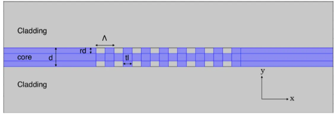
Considering a single mode photonic wire on 1 um thick SOI as shown in Fig. 3.1. silicon (Si) core layer has 260 nm thickness and its width (d) has been fixed at 500 nm so that it supports only a single fundamental TE mode at 1.52 um wavelength operation and the materials used have refractive indices 3.47 for Si and 1.45 for SiO2.
The description of this sidewall grating design is formed by the parameters: grating period (Λ), recess depth (rd) and tooth length (tl). These three parameters are considered as free parameters because of their spectral effects on the transmission and reflection profiles of the device.
3.1.1 2D Model
In the characterization of functional behavior of the photonic integrated circuits (PICs), numerical design approaches, such as FEM, FDTD, play a critical role in modeling and analysis. Before the fabrication processes, such approaches can be implemented by the software packages under the approximations. The affinity of experimental and simulation results of a device depends on various factors such as fabrication techniques, technology limitations and computational modeling. In order to have accurate numerical outcomes, 3D analysis is required. However, simulation of 3D structures has some drawbacks; in practice, longitudinal size of a PIC can vary from micrometers to millimeters. In this point, the model has to be adapted to the actual dimensions of the fabricated structure. Therefore, dimensions of the 3D modeling may be restricted according to the computational efforts, in this case time becomes an important parameter. The other issue is that 3D simulation requires much more memory with respect 2D due to the need of volumetric mesh. Therefore, this drawback may limit implementation of the realistic structures.
If it is needed to underline the point in comparison of different dimensions, simulation of 2D structures can be considered to obtain the preliminary results for the reason of having a general opinion about the features of the device. Thereby, it is possible to save time and control whether optical properties of the desired component are as expected.
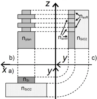
The Effective Index Method is a technique to reduce the dimensionality from 3D to 2D [22]. The basic idea of the method is to approximate two-dimensional waveguide by a three-dimensional one with an effective index profile that can be obtained from the geometry and the effective index profile of the original structures. Fig. 3.2 shows a representation of the transition from cross-section view of 3D structure to 2D plan view and axial cross section [23].
Figure 3.2: Three orthogonal views of the photonic wire Bragg grating: waveguide cross section (a), plan view (b), axial cross section (c).
Here, approximated geometries are the plan view and the axial view. In this thesis, only plan view is considered for the simulations in 2D. According to the reduced model in 2D, the refractive indices of the core and cladding are changed. Basically, the new refractive index of the core is the effective refractive index of the 3D structure for 𝜆= 1.52 𝜇𝑚. As a result, new refractive indices in 2D design, instead of 3.47 for silicon and 1.44 for SiO2, are substituted as 2.97 for the core and 1 for the
cladding.
(a) (b)
Figure 3.3: Comparison of 3D and 2D by FDTD (a) and same device analyzed in 2D by FEM (b).
As an example, a 16-period photonic wire Bragg grating that has 390 nm grating period, 120 nm recess depth and 195 nm (which means %50 duty cycle) is simulated and transmission and reflection spectrum are illustrated in Fig. 3.3 with comparison 2D and 3D cases of FDTD obtained from ref. [23](a) and the same device, simulated by FEM (b). It can be observed that (a) and (b) have similar transmission characteristics, however do not superimpose perfectly due to different mesh elements. Beside this, results of 2D and 3D structures have the same stop-band characteristics.
3.2
Modeling in Comsol Wave Optics
In this section, the fundamentals of modeling in Comsol are introduced. Comsol is a finite element analysis solver that used in various physics and engineering application. In particular, the Comsol Wave Optics package can be utilized for solving electromagnetic wave propagation in the optical applications.
3.2.1 Physics Interfaces
Comsol offers different physics interfaces according to the problem domain, from chemistry to heat transfer and acoustics, etc. In our case, the study domain is the electromagnetic wave in frequency domain (ewfd) under the wave optics section. Since the purpose of the analysis is finding propagation constant and possible guided modes, boundary mode analysis is chosen as the study type.
3.2.2 Geometry
Full geometry of the structure is consisted of the rectangular shapes only. Fig. 3.4 shows the grating and its design parameters.
3.2.3 Perfectly Matched Layer
Perfectly Matched layer (PML) is a theoretical concept that presents a domain that absorbs the waves without producing reflections regardless the incident angle. It is needed to distinguish that PML is not a boundary condition, it is a domain and mostly used to truncate the computational region. Thus, the wider PML width the higher absorption is performed. As shown in Fig.3.5, the region of the interest is surrounded by the PML domains.
Figure 3.5: PML implementation.
3.2.4 Frequency Domain Analysis
This interface has four basic components, wave equation, perfect electric conductor, initial values and ports [25]. The wave equation is determined as:
with
where n is the refractive index, 𝜅z is the out-of-plane wave number and 𝜅0 is the wave
number of free space and defined as .
r ⇥ (r ⇥ E)
20n
2E = 0
(3.1)
E(x, y, z) = ˜E(x, y)exp( jzz) (3.2)
Perfect Electric Conductor (PEC) is a special case of the electric field boundary condition that sets the tangential component of the electric field to zero and defined as:
by means of that any current flowing into the boundary is perfectly balanced by induced surface currents. The tangential electric field vanishes at the boundary. Initial value assumes that Ex, Ey and Ez are set up to zero as initial electric fields. And
finally, the ports are placed where the wave excites with specified power and mode. In our case, ports are set as numeric because the modes are defined by the boundary conditions. As shown in Fig. 3.6, red arrows represent the port 1 and port 2 and their directions indicate the direction of the excited wave. In this case, to make the wave flow through the core, the port orientations must be set as reverse.
Figure 3.6: Port configurations and dimensions with 3 𝜇𝑚 PML width, 2𝜇𝑚 input and output waveguides, 1 𝜇𝑚 the width of the inner cladding and 3.75 𝜇𝑚 the width of the outer cladding.
3.2.5 Mesh
Mesh is one of the most important parameters in order to obtain accurate results. Mesh configuration determines the resolution the finite element. Therefore, FEM
approximates the solution within each element depending on the mesh element quality. However, there is a trade off between quality of the mesh element and solving time. As a result, the finer mesh the more accurate solution, but the more computational time is required.
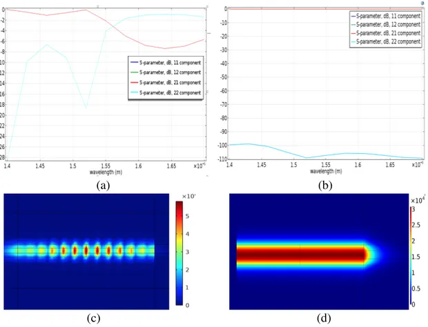
An example: considering two identical straight photonic silicon waveguides with 400 nm core width. The waveguides are simulated for the fundamental TE mode with two different mesh configurations in which the type of the element is the same for both, however, one has 12 times finer (more resolution) mesh elements than the other one. The one that has finer mesh performs exactly as expected while, the other one performs incorrectly.
(a) (b)
(c) (d)
Figure 3.7: Reflection (S11 and S22) and transmission (S12 and S21) spectrum of the single mode straight waveguides and their Electric field norms with courser mesh (a) and (c) and finer mesh (b) and (d), respectively. Left hand side represents bad solution while the right hand side represents correct solution.
Chapter 4
This chapter presents the transmission matrix method in the sense that periodic and almost periodic photonic structures can be characterized via this method. Some of the theory of the Scattering and Transmission parameters is given by considering a two-port network. At the end of the chapter, improtant properties of a straight waveguide are discussed in terms of its scattering matrices.
Transmission Matrix Method
4.1 Two Port Network
At optical frequencies, voltages and currents are difficult entities to measure, and it is necessary to define a new representation that is called Scattering parameters (S-parameters) [26]. S-parameters are associated to frequency and wave propagation representing the relationships between incident and reflected waves at ports, and the input and output planes of the device are orthogonal to the propagation direction of the waves.
Let a1, a2 and b1, b2 are the values of incident and reflected waves. Two-port network
is represented in Fig.4.1.
Figure 4.1: Representation of a two-port network.
a
1a
2b
1b
2 Two-Port Network Port 1 Port 2The field coefficients of the fields in both forward and backward directions were introduced in the Chapter 2 (see the coupled mode theory) in the equation (2.23) and (2.34). By using these equations, the matrix form of the S-parameters can be defined as:
where the scattering matrix (S-matrix) is
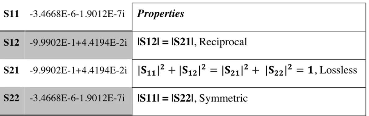
The matrix elements S11, S12, S21, S22 represent S-parameters. The parameters S11 and
S22 have the meaning of reflection coefficients, and S21, S12, the meaning of
transmission coefficients. These parameters are used to get optical features of a device because the parameters are represented by the dimensionless complex numbers that represent amplitude and phase of the waves.
According to the (4.1) and (4.2), the relationship between reflection/ transmission coefficients and incident/reflecting waves is defined as:
S11 and S22 are input and output reflection coefficients, respectively, and S12 and S21
are the reverse and forward transmission coefficients, respectively. The actual measurements of the S-parameters are made by connecting to a matched load with the value of characteristic impedance (Z0) of the transmission line, which is usually 50 Ω
[27]. Measurement of S11 and S21 are made with the input of port1 is terminated by Z0
and similarly, the input of port 2 is terminated for S22 and S12.
A device can be categorized according to its S-parameters relationships such as lossless, reciprocal and symmetric. If a device is lossless, then the relationship holds |𝑆!!|!+ |𝑆
!"|! = |𝑆!"|!+ |𝑆!!|! = 1. If a device is reciprocal, then the relationship
holds 𝑆!"= 𝑆!" and finally, if a device is symmetric, then the relationship holds
𝑆!! = 𝑆!!.
b
1b
2= [S]
a
1a
2(4.1)
[S] =
S
11S
12S
21S
22(4.2)
S
11=
b
1a
1,
S
22=
b
1a
2(4.3)
S
21=
b
2a
1,
S
12=
b
2a
2(4.4)
4.1.1 Obtaining S-Matrix using Comsol Wave optics Module
The scattering parameters are the basis of the transmission matrix method, will be introduced later, such that in order to apply this method to study periodic and almost periodic structures, S-parameters should be obtained in an accurate way. For this purpose, the test for correctness of the simulation is carried out for a straight silicon waveguide in 2D.
According to the Comsol wave optics user guide [28], the calculation of S-parameters is carried out as; Comsol performs eigenmode analysis to convert Electric field patterns on the ports to scalar complex numbers. Further, these calculated E1 and E2
field patterns of the fundamental modes are normalized with respect to the integral of the power flow across each port cross section, respectively. The port excitation is applied using the fundamental eigenmode. The computed electric field Ec on the port
consists of the excitation plus the reflected field. S-parameters at Port 1 and Port 2 are given by
where A1 and A2 are the areas of ports. Similarly, S22 and S12 are calculated by
exciting port 2 in the same way.
In the thesis, all devices such as straight waveguides, Bragg gratings and tapers are investigated in single mode regime (the geometrical dimensions of the cores are adjusted to allow only for the fundamental modes in a certain frequency range) therefore it is possible to explain reflection and transmission parameters in terms of the power flow through the ports. However, this definition is only the absolute values of the S-parameters defined above equations and does not have any phase information.
The definition of the S-parameters in terms of the power flow is given as:
𝑆!! = !"#$% !"#$"%&"' !"#$ !"#$ !!"#$% !"!"#$%& !" !"#$ ! (4.5)
𝑆!" = !"#$% !"#$%"&"! !" !"#$! !"#$% !"#!$%"& !" !"#$ ! (4.6)
4.2 Properties of Photonic wire Straight Waveguide
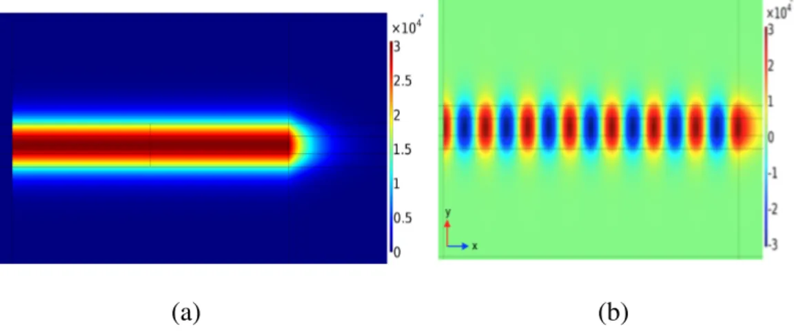
In this section, an example of a silicon photonic straight waveguide is presented in 2D. A silicon straight waveguide with 400 nm core width and 2 um long is simulated. The ports excite the field in the x propagation direction with the fundamental mode at the wavelength 1.52 𝜇𝑚 as shown in Fig. 4.2. and the materials, silicon core and cladding have the refractive indices 2.97 and 1, respectively.
(a) (b)
Figure 4.2: Electric Field Norm of the straight waveguide (a) Ez (b).
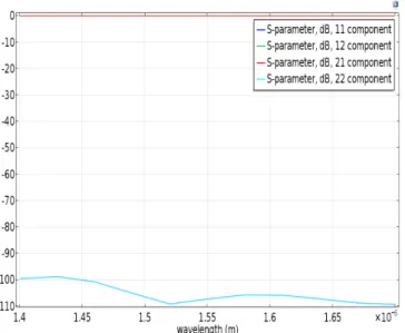
The waveguide is studied only in single mode operation, thus there is no radiation loss. Well-guided mode can be seen in (a) because the maximum value of the electric field norm is centered in the core. This device is operated in the wavelength range of 1.4 𝜇𝑚 and 1.7 𝜇𝑚 and S-parameters are illustrated in the Fig. 4.3. As expected from theory, S12 and S21 superimpose that means the device is reciprocal. Further, it is also
symmetric because of superimposing of S11 and S22. To check whether it is lossless,
we need to perform the condition; |𝑆!!|!+ |𝑆!"|! = |𝑆!"|!+ |𝑆!!|! = 1. The
S-parameters at 𝜆=1.52 𝜇𝑚 are reported in the table 4.1. Preliminary results demonstrate that properties of the S-parameters meet the requirement the properties of the straight waveguide insingle mode operation as in theory.
Table 4.1: S-parameters of the straight photonic wire at 𝜆=1.52 𝜇𝑚 and its properties Furthermore, there is the last check to be considered that is the propagation constant. In Comsol, the method for seeking TE or TM modes is determined by the effective index method. It is important to verify whether simulated results are correct; the propagation constant obtained from the software can be compared to theory. To do so, a numerical tool that has been developed in the DEI (department of electrical, electronic and information engineering) at the University of Bologna is used. This tool finds effective index accurately with given specifications such as refractive index of the core and cladding, width of the core and frequency. The comparison both results from Comsol and this tool are reported in Table 4.2. Generally speaking, the effective index method is useful for determination of dispersion curves in a rectangular shape waveguide when the modes are near cutoff. In case of the guided mode is present, the propagation constant (when attenuation is zero) has only the phase constant defined as [29].
𝛽 = 𝑛!""!!! (4.7) where neff is the effective index and 𝜆 is the operation wavelength.
*Theory refers the solution of a numeric tool developed at DEI
Table 4.2: Comparison of the effective indices for TE modes at 𝜆=1.52 𝜇𝑚.
S11 -3.4668E-6-1.9012E-7i S12 -9.9902E-1+4.4194E-2i S21 -9.9902E-1+4.4194E-2i S22 -3.4668E-6-1.9012E-7i Properties |S12| = |S21|, Reciprocal |𝐒𝟏𝟏|𝟐+ |𝐒 𝟏𝟐|𝟐 = |𝐒𝟐𝟏|𝟐+ |𝐒𝟐𝟐|𝟐= 𝟏, Lossless |S11| = |S22|, Symmetric
TE Modes Fundamental Second Order
neff in Theory* 2.6653618164 1.6332953613
Figure 4.3: S-parameters of the single-mode straight photonic wire in dB. In this section, some important properties of the S-parameters of a two-port network is presented in order to extract spectral behavior of the analyzed optical device. However, S-parameters are useful for determining the characteristics a single network. For example, in order to characterize a cascade system, it is needed to define a new concept that is called the transmission parameters.
4.2.1 Transmission Matrix
The transmission parameters, also called Transmission scattering parameters or T-parameters, provide analyzing the cascaded network systems. It is important to distinguish that T-parameters do not refer transmission or reflection coefficients, they represent only a treatment to analyze cascaded systems. These parameters are defined in such a way that input waves a1 and b1 are dependent variables while a2 and b2 are
independent. T-parameters are given by
A cascade network can be described as shown in Fig.4.4 that two networks share the same ports for the incident and reflected waves.
Figure 4.4: A cascade network system consisted of two networks.
a
1b
1=
T
11T
12T
21T
22
b
2a
2(4.8)
In detail, the outgoing wave of the first network (b2) is the incoming wave of the
second network (a3) and so on. In this network system, the first network (T1) is built
as
Similarly, the second network (T2) is defined as
and finally the overall T-matrix can be obtained by multiplying [T1] and [T2]
or
The relationship between the S and T parameters can be developed from (4.1) and (4.8):
and
In the work of the thesis, the conversion from S-parameters to T-parameters or vice versa is carried out by a Matlab code that implements the conversion exactly as defined in (4.13) and (4.14).
a
1b
1=
T
111T
121T
211T
221
b
2a
2(4.9)
a
3b
3=
T
112T
122T
212T
222
b
4a
4(4.10)
a
1b
1=
T
111T
121T
211T
221
T
112T
122T
212T
222
b
4a
4(4.11)
a
1b
1= [T
1][T
2]
b
4a
4(4.12)
T
11T
12T
21T
22=
2
4
1 S21 S22 S21 S11 S21S
21 S11S22 S213
5
(4.13)
S
11S
12S
21S
22=
2
4
T21 T11T
21 T21T12 T11 1 T11 T12 T113
5
(4.14)
4.3 Definition of TMM for the segmented waveguides
Basically, a photonic wire Bragg grating has three components in terms of geometry; two straight waveguides are connected each other with a centered grating as shown in Fig. 4.5. The T-matrix of the entire structure is represented by the global matrix Tg,1.
Ts and T1 are the T-matrices of the straight waveguide with one period grating.
Figure 4.5: The sketch of 1-period photonic wire Bragg grating, blue part represents the core while the gray part represents the cladding.
The overall-matrix is given by:
To extract T1 equation, it is needed to obtain S-matrix of the straight waveguide,
which has been introduced in the previous section, and plus the S matrix of the whole structure. Then it is possible to convert S-matrices to T-matrices by using equation (4.13). Further, T1 can be get from:
For the further periods, the same procedure can be done as an example of a 2-period grating is illustrated in Fig. 4.6.
Figure 4.6: The sketch of 1-period photonic wire Bragg grating.
T
g,1= T
s⇤ T
1⇤ T
s(4.15)
The relationship between global T-matrix of the 2-period Bragg grating waveguide and the grating junction can be written as,
where, in fact
Substituting the equation (4.16) to the (4.18), the overall T-matrix of the 2-period structure can be defined as 1-period:
Finally, it is possible to developed the generalized T-matrix by considering the equations (4.15) and (4.19) and it is given by:
where N is the number of grating period.
To sum up, it is shown that the transmission matrix method is a tool that allows examining periodic photonic structures such that by knowing the properties of a single period, the properties of the entire component can be calculated. For this reason, the features of the TMM can used to build up a design tool [32] to deal with long periodic structures for determination of those of their transmission and reflection characteristics. However, it is needed to take into account that all calculations in this thesis are made by using numerical methods therefore the error of calculated and simulated results is inevitable. The error 𝜀 of the calculated and simulated T and S parameters can be defined by the following equations:
𝜀
!"!=
!!",!!|!!",!! |
|!!",!|
(4.21)
where 𝑇!",! is the simulated result and 𝑇!",!! is the calculated result
𝜀
!"!=
!!",! !|!!",!! |
|!!",!|
(4.22)
where 𝑆!",! is the simulated and 𝑆!",!! is the calculated result, i = 1,2 , j= 1,2 , andS11, S12, S21, S22 are the input reflection coefficient, reverse transmission gain, forward
transmission gain and output reflection coefficient, respectively.
T
g,2= T
s⇤ T
2⇤ T
s(4.17)
T
2= T
12(4.18)
T
g,2= T
s⇤ T
12⇤ T
s(4.19)
An example has been made in order to study the impact of the number of periods on the error. Fig. 4.7 shows the error of S-parameters in percentage of a Bragg grading, with 400nm core width, according to different periods up to 64 at 1.52 𝜇𝑚. It is seen from the graph that the error of the transmission parameters has a maximum value of approximately 3% when N=32 then decreases. On the other side, the error of the reflection parameters increases steadily up to almost 0.5 % by increasing the number of periods.
Figure 4.7: Error of |S| parameters vs N at 1.52 𝜇𝑚.
Up to now, the transmission matrix method has been developed for photonic wire Bragg gratings with 50% duty cycle periodicity meaning that the period of the grating is composed of half core and half cladding. In the next chapter, the approach will be tested with various changes in design parameters such as grating period, duty cycle, tooth length of the grating etc.
Chapter 5
This chapter provides the results of the TMM applied to some specific structures in both 2D and 3D. The calculated and simulated S-parameters of studied devices are reported. Additionally, two taper applications have been performed and their impacts on the transmission characteristics are discussed. Finally, the verification of the developed design approach in 3D is presented.
Application of TMM in 2D and 3D
5.1 The TMM applied to periodic structures in SOI in 2D
A general sketch of a photonic wire Bragg grating with the design parameters is illustrated in Fig. 5.1. Basically, there are four design parameters, also called free parameters, to play with, except the core width because it is fixed at 400 nm to operate the waveguide in single mode operation. The refractive indices of the core and cladding are 2.97 and 1 respectively.
Figure 5.1: The schematic of periodic structure with design parameters.
The recess width R and the grating period Λ are the parameters that construct a single period and then single periods form up the whole grating structure by repeating themselves. It was mentioned in the Chapter two that the intensity of reflection raises by increasing the length of the grating L and it holds L = NΛ where the N is the number of periods. In order to extract correctly the effects of each parameter on the device properties, the other parameters should be fixed. For this reason, the default design parameters are chosen as 16 periods, 390 nm grating length, 120 nm recess
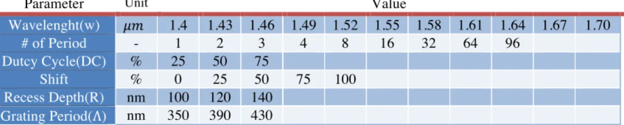
the table 5.1. First of all, the design has been implemented in 2D for the verification of the TMM. Once the approach is tested and verified that it allows interpreting the functional behavior of a device in further periods by using only the first period, it is possible to extend the design in 3D for obtaining more accurate solutions without dimensional restrictions. To do so, the calculated and simulated |S| parameters are plotted together to make the comparison between them in a certain wavelength range that is varying between 1.4 𝜇𝑚 and 1.7 𝜇𝑚. The range of the wavelength is sampled with the 0.03 𝜇𝑚 thus there are 11 wavelengths that have been considered for each parameter. It is notable that the S and T parameters are complex numbers and so they have both magnitude and phase information. However, since we are interested in magnitude spectra, only argument of scattering |S| and transmission |T| parameters are considered. Furthermore, the structures are reciprocal and symmetric but no more lossless because of scattering off from sidewalls of the waveguide though scattered fields are absorbed as much as possible by the PML domains. As a result, scattered fields do not influence the results as the back reflections from the perfect electric conductor (PEC) boundaries. As a consequent of this point, it can be said that |S11| = |S22| and also |S12| = |S21|. In this case, there is no need to plot both |S11| and |S22| or |S21| and |S12| at the same time, at least in the test of the number of periods therefore as a notation; |S12| represents the transmission coefficient while |S11| represents the reflection coefficient.
Parameter Unit Value
Wavelenght(w) 𝜇𝑚 1.4 1.43 1.46 1.49 1.52 1.55 1.58 1.61 1.64 1.67 1.70 # of Period - 1 2 3 4 8 16 32 64 96 Dutcy Cycle(DC) % 25 50 75 Shift % 0 25 50 75 100 Recess Depth(R) nm 100 120 140 Grating Period(Λ) nm 350 390 430
Table 5.1: The list of the tested design parameters by the TMM.
5.1.1 Analysis of the number of periods
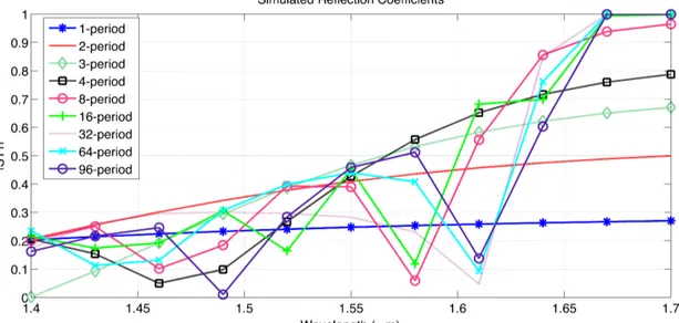
The filtering characteristics of a Bragg grating are directly linked to its length, the grating period and the recess width. The selection of which wavelengths will be reflected and which ones will be transmitted can be arranged by changing its number of the periods when the other parameters R and Λ are fixed. Here, the decision of how many periods are needed for filtering is taken by testing the structures with different periods. To run faster simulations, only a single band edge is considered: the better the filter, the sharper the band edge. The S-parameters are obtained starting from one period up to 96 periods. Fig. 5.2 and Fig. 5.3 show the simulated transmission and reflection coefficients for different number of periods. The decision of the default
number of the period is taken according to filtering features of the gratings: it is clear that 1-period grating do not filter almost any wavelength and as thenumber of periods increases, the grating becomes selective. The transition from transmission to reflection becomes sharper after 16-period and only after this critical point some wavelengths get reflected almost totally.
Figure 5.2: The simulated transmission coefficients |S12| vs number of the periods.
Figure 5.3: The simulated reflection coefficients |S11| vs number of periods.
The calculation of the T and S parameters was introduced in the previous chapter. By using the equation (4.20), it is possible to calculate the scattering and transmission
single run and the results those obtained by using the equation (4.20). It is obvious that the coefficients superimpose perfectly for the first period. Because, the first period has the reference T-matrix in which all otherT-matrices are calculated from it. As it is explained in the design procedure, after T-matrix calculations are complete, they are reconverted into the S-matrices by using again the Matlab code. It is demonstrated that the calculated results by the TMM and the simulated ones are in good agreement especially until 96 periods. Nevertheless though both results do not overlap perfectly, the spectral behaviors of the calculated and simulated coefficients are similar (consider that the equation T1
96
= T96 is performed for 96 periods).
Figure 5.4: The plots of the simulated and calculated results of the transmission and reflection coefficients for different number of periods.
Since the 16-period grating has been chosen as the reference structure, it might be better to look its T parameters in an extended plot as shown in Fig. 5.5. It is important to underline that T parameters do not need resemble S parameters because of different conceptual point of view. Here, there is only one issue to be considered that how well calculated and simulated T parameters superimposing each other. In addition, results of 16-period grating waveguide are plotted in dB in Fig. 5.6. It can be seen from the graph that reflection and transmission coefficients have a cross section around -3dB between the wavelength range of 1.6 𝜇𝑚 and 1.65 𝜇𝑚.
Figure 5.5: The calculated and simulated T-parameters of the 16-period grating.
Figure 5.6: The transmission and reflection coefficients in dB with the calculated and simulated results.
5.1.2 Analysis of the Duty Cycle
Duty cycle (DC) refers the ratio between the length of the core grating tooth (tl2) and
the length of the grating period (Λ) and it holds DC = tl2/ Λ. An example of 75% DC
cycle is illustrated in Fig. 5.7. It can be written from the figure that tl1+tl2 = Λ where
tl1 is the length of the cladding grating tooth. In this work, three different DCs have
been tested by the TMM that are 25%, 50% and 75%. All other design parameters were fixed at their default values as Λ= 390 nm, 400 nm core width, recess depth rd= 120 nm and 16-period of the grating.
Figure 5.7: The example of %75 DC with two periods and the Duty Cycle parameters. Grating Period (Λ) Duty Cycle (DC) tl1 tl2
390 nm %25 292.5 nm 97.5 nm
390 nm %50 195 nm 195 nm
390 nm %75 97.5 nm 292.5 nm
Table 5.3: DC configurations employed with fixed grating period.
By using different DC configurations, it is possible to build up a taper that its DCs linearly increase. For example, a taper configuration, which will be introduced later, can be made by cascading different DCs that linearly increase as from 10% to 50%. However, at this moment, the purpose of the investigation of different DC configurations is extracting the effects of DC on the optical property of a device. For this motivation, a 16-period grating is implemented with the configurations listed in Table 5.3. and relevant outcomes are presented in Fig. 5.7, 5.8, 5.9 and 5.10 together the results of applied TMM.
Figure 5.8: Calculated and Simulated Scattering parameters of 25% DC.
Figure 5.9: Calculated and Simulated Scattering parameters of 50% DC.
As it can be seen from the graphs, the transmission matrix method applied to different duty cycles is successfully tested and calculated results from the TMM are in a good agreement with the simulated ones. It is also noticed that DC has an impact on the transmission coefficients (see Fig. 5.7) such that a 16-period grating with 25% DC do not exhibit any filtering behavior while the structures with 50% and 75% DC reflect wavelengths greater than approximately 1.58 𝜇𝑚 . As a result, having the S parameters of a grating with different DC may help in constructing a specific taper which performs in mode conversion or low-loss fiber to optic applications.
5.1.3 Analysis of the Shift
The shift is a perturbed case in which the lower side grating is forwarded with respect to the upper side grating. An example of a 25% shifted grating period with 50% DC is shown in Fig. 5.10.1. The SHF is the shifting parameter representing the length of forwarded domain. Therefore the shift ratio in percentage can be defined as
Shift (%) = SHF/ Λ*100
Figure 5.10.1: The example of 25% shifted grating in the lower side
In shifting analysis, four different shifted gratings are studied, and these are 25%, 50%, 75% and %100. Fig. 5.10.2 shows the simulated outcomes of different shifts and according to this graph, interestingly, 100% shifts makes the device almost lossless in the given frequency range as in case of straight waveguide. From this property, it can be said that a grating that its upper and lower gratings are shifted by 100% with respect to each other exhibits transmission characteristics as a straight waveguide. On the other hand, other shifting parameters have a great impact on wavelength selectivity such that pass-band window reduces with increasing shift until 75%. In addition, Fig. 5.10.3 collects all calculated and simulated outcomes of shifting processes. It can be noticed from the graphs that the developed design approach fails when the shift is present. Especially, when the percentage of the shift is increased the error becomes enormous.
Figure 5.10.2: Simulated Transmission Coefficients in dB for different SHFs.
(a) (b)
(c) (d)
Figure 5.10.3: Simulated and calculated results of a 16-period grating with different SHFs, 25% (a), 50% (b), 75% (c), 100% (d)
The possible reason of the failure in the application of the TMM to the shifted structures, according to author’s opinion, can be due to the distorted geometrical symmetry along the propagating direction, in this case it is the x direction, may cause the extremely irrelevant transmission characteristics in different periods. Because, normally, the transport property of a single period grating should some how contain the information about the transport property of the further periods. However, in the
the applicability of the TMM for periodic structures may depend on the periodicity symmetry along the longitudinal axis. In any matter, until detailed investigation of this issue is done, it is hard to comment that is why, finding a clear answer of this phenomenon will be a part of the future work.
5.1.4 Analysis of the Recess Depth
In this analysis, three different recess depths have been studied. As shown the transmission coefficients in dB in Fig. 5.11, the greatest recess depth, which is 140 nm, has more impact on the transmission profile of the device than the others. Regarding the other design parameters, the same default configurations are still valid: 50% DC, 16 periods, 390 nm grating period. The other figures 5.12 and 5.13 present the results of the TMM applied for 100 nm and 140 nm recess depths. Displaying the results of the 120 nm is not needed because it is already demonstrated in the analysis of the duty cycle (See Fig. 5.9).
Figure 5.11: Transmission Coefficients of three different recess depths.
Figure 5.13: The scattering parameters of 140 nm recess depth.
It can be clearly seen from Fig. 5.2 and 5.3 that the grating with 100 nm recess depth does not filter any wavelength, its functional behavior resembles the property of the straight waveguide. On the other hand the grating with 140 nm recess depth exhibits filtering, starting from around 1.51 𝜇𝑚.
5.1.5 Analysis of the Grating Period
The grating period as a design parameter is investigated for three values. The length of the grating period is another important parameter that affects the selectivity of the device. As seen the transmission coefficients of 350, 390 and 420 nm grating length in Fig.5.14, the longest period has almost no selectivity and while the length decreases, the grating reflects the wavelengths from a certain wavelength which is 1.49 𝜇𝑚 with near -3dB loss for the 350 nm and 1.68 𝜇𝑚 for the 390 nm grating.
![Figure 1. Number of scientific publication from (silicon AND photonic) search, in ISI Web of Science [6]](https://thumb-eu.123doks.com/thumbv2/123dokorg/7434710.99885/10.892.283.638.487.741/figure-number-scientific-publication-silicon-photonic-search-science.webp)