Autore:
Gianni Antichi _______________
Relatori:
Prof. Stefano Giordano ___________________ Prof. Franco Russo ___________________
Fast Packet Processing on High
Performance Architectures
Anno 2011 SSD ING-INF/03
UNIVERSITÀ DI PISA
Scuola di Dottorato in Ingegneria “Leonardo da Vinci”
Corso di Dottorato di Ricerca in
Ingegneria dell’Informazione
To my parents Renzo & Graziella & to my grandparents Ernesto, Piera, Lido & Fedora. Thanks for all you have done.
First of all, I want to say thanks to my friends. I shared with you many wonderful moments during these years. Thanks Lorenzo, Matteo, Alessio, Stefano, Sabina, Daniele, Alessandra, Laura, Frang´e, Francesco, Paolo, Gioia and Alfredo. I also want to thank all the people in my research group. Thanks Christian, Gregorio, Andrea et al. I spent with you a lot of good moments and a lot of good meals. I would like to acknowledge Fabio and Domenico. Thanks guys. We were an incredible team. Hope to work another time with you in the future. I want to thank my tutors prof. Stefano Giordano and prof. Franco Russo. I am grateful to Dr.Andrew Moore for giving me the opportunity of interning in the Computer Lab at University of Cambridge where i met a lot a good people and learn a lot of things.
Sommario
La rapida crescita di Internet e la nascita sempre pi´u veloce di nuove ap-plicazioni di rete hanno portato ad una difficolt´a sempre maggiore nello sviluppo di reti IP ad alta velocit´a con supporto anche per la qualit´a del servizio (QoS). Per tale motivo la classificazione dei pacchetti e la intru-sion detection hanno assunto un ruolo chiave nelle reti di comunicazione moderne al fine di fornire QoS e sicurezza. In questa tesi mostriamo al-cune fra le pi´u avanzate soluzioni per lo svolgimento efficiente di queste operazioni. Cominciamo introducendo il NetFPGA e i Network Proces-sors come piattaforme di riferimento sia per la progettazione e lo studio che per l’imple-mentazione degli algoritmi e, in generale, delle tecniche che sono descritte in questa tesi. L’aumento della capacit´a dei link ha ridotto il tempo a disposizione dei dispositivi di rete per l’elaborazione dei pac-chetti. Per questo motivo, mostriamo in questo lavoro differenti soluzioni che, o attraverso operazioni di “randomizzazione” ed euristiche o con la costruzione intelligente ed efficace di macchine a stati finiti, permettono ai nodi di rete di effetturare operazioni di IP lookup, classificazione e deep packet inspection in modo veloce su piattaforme ad alta velocit´a come i Network Processor o il NetFPGA.
The rapid growth of Internet and the fast emergence of new network ap-plications have brought great challenges and complex issues in deploy-ing high-speed and QoS guaranteed IP network. For this reason packet classification and network intrusion detection have assumed a key role in modern communication networks in order to provide Qos and security. In this thesis we describe a number of the most advanced solutions to these tasks. We introduce NetFPGA and Network Processors as reference plat-forms both for the design and the implementation of the solutions and algorithms described in this thesis. The rise in links capacity reduces the time available to network devices for packet processing. For this reason, we show different solutions which, either by heuristic and randomization or by smart construction of state machine, allow IP lookup, packet clas-sification and deep packet inspection to be fast in real devices based on high speed platforms such as NetFPGA or Network Processors.
Contents
Introduction 1
1 Introduction to FPGA-based Networking Boards and Network
Pro-cessors 3
1.1 FPGA-Based Networking Boards . . . 3
1.1.1 What is an FPGA? . . . 4
1.1.2 FPGA Design and Programming . . . 4
1.1.3 The Combo6 . . . 5
1.1.4 The NetFPGA . . . 6
1.1.4.1 Architecture . . . 6
1.1.4.2 Reference Pipeline Details . . . 7
1.1.4.3 Life of the Packet . . . 8
1.1.4.4 Register Pipeline . . . 9
1.2 Comparison among Network Processor Platforms . . . 10
1.2.1 Multi-chip Pipeline (Agere) . . . 10
1.2.1.1 Architecture . . . 10
1.2.1.2 Processors and functional units . . . 11
1.2.1.3 Memory . . . 12
1.2.1.4 Programming support . . . 12
1.2.2 Augmented RISC Processor (Alchemy) . . . 14
1.2.2.1 Architecture . . . 14
1.2.2.2 Processors and functional units . . . 14
1.2.2.3 Memory . . . 15
1.2.2.4 Programming support . . . 15
1.2.3 Embedded Processor Plus Coprocessors (AMCC) . . . 15
1.2.3.1 Architecture . . . 15
1.2.3.2 Processors and functional units . . . 16
1.2.3.3 Memory . . . 16
1.2.3.4 Programming support . . . 16
1.2.4 Pipeline of Homogeneous Processors (Cisco) . . . 16
1.2.4.1 Architecture . . . 16
1.2.4.2 Processors and functional units . . . 17
1.2.4.3 Memory . . . 18
1.2.4.4 Programming support . . . 18
1.2.5 Configurable Instruction Set (Cognigine) . . . 18
1.2.5.1 Architecture . . . 18
1.2.5.2 Memory . . . 19
1.2.5.3 Programming support . . . 20
1.2.6 Pipeline of heterogeneous processors (EZchip) . . . 20
1.2.6.1 Architecture . . . 20
1.2.7 Extensive and Diverse Processors (IBM) . . . 21
1.2.7.1 Architecture . . . 21
1.2.7.2 Memory . . . 23
1.2.7.3 Programming support . . . 23
1.2.8 Flexible RISC Plus Coprocessors (Motorola) . . . 23
1.2.8.1 Architecture . . . 23
1.2.8.2 Programming support . . . 25
1.3 Intel IXP2XXX Network Processors . . . 25
1.3.1 General Structure . . . 25
1.3.2 The Intel XScale . . . 26
1.3.3 Microengines . . . 26
1.3.3.1 Threads . . . 27
1.3.3.2 Registers . . . 27
1.3.3.3 Signaling . . . 28
1.3.3.4 Local Memory . . . 29
1.3.3.5 Content-Addressable Memory and CRC . . . 29
1.3.4 Memories . . . 29
1.3.5 Media Switch Fabric . . . 30
1.3.6 SHaC . . . 30
1.3.7 Intel IXA Portability Framework . . . 31
1.3.7.1 Microblocks and Core Components . . . 31
1.3.7.2 XScale/microengines interactions . . . 31
1.3.8 IXA SDK . . . 32
1.3.8.1 Assembly for microengines . . . 32
1.3.8.2 Constructs . . . 33 1.3.8.3 Virtual registers . . . 33 1.3.8.4 Microengine-C . . . 34 1.3.9 Developer’s Workbench . . . 34 1.3.9.1 Scripting . . . 34 1.3.10 ENP-2611 . . . 35
2 Deep Packet Inspection 37 2.1 δFA: An Improved DFA construction for fast and efficient regular ex-pression matching . . . 38
2.1.1 Related Work . . . 39
2.1.2 Delta Finite Automaton . . . 40
2.1.2.1 Motivation through an example . . . 42
2.1.2.2 Definition of δFA . . . 42
2.1.2.3 Construction . . . 43
2.1.2.4 Lookup . . . 44
2.1.3 Application to H-cFA and XFA . . . 45
2.1.4 Compressing char-state pairs . . . 47
CONTENTS
2.1.4.1 Indirection Table Compression . . . 48
2.1.5 δFA with C-S . . . 49
2.1.6 Implementation . . . 50
2.1.7 Experimental Results . . . 51
2.2 Second order delta enconding to improve DFA efficiency . . . 54
2.2.1 The Main idea of δ2FA . . . 54
2.2.1.1 Lookup . . . 56
2.2.1.2 Construction . . . 56
2.2.2 Experimental Results . . . 58
2.3 Homomorphic encoding of DFAs . . . 60
2.3.1 Related works . . . 60
2.3.2 An efficient representation for DFAs . . . 61
2.3.3 The look for an effective Homomorphism . . . 62
2.3.4 Optimizations . . . 64
2.3.4.1 Permutation for LPM . . . 64
2.3.4.2 Bitmap trees . . . 65
2.3.4.3 The overall algorithm . . . 66
2.3.5 The k-step DFA . . . 67
2.3.6 Results . . . 67
2.4 Sampling techniques to accelerate regular expression matching . . . . 68
2.4.1 Sampling DFAs . . . 70
2.4.1.1 Motivation . . . 70
2.4.1.2 A Motivating Example . . . 71
2.4.1.3 Taxonomy of DFA Sampling . . . 71
2.4.2 Regex sampling rules . . . 72
2.4.2.1 Regex rewriting . . . 72
2.4.3 Constant Period Sampling . . . 73
2.4.3.1 First stage: Sampled DFA . . . 73
2.4.3.2 Second stage: Reverse DFA . . . 75
2.4.3.3 Possible implementations . . . 79
2.4.3.4 Dealing with DoS attacks . . . 79
2.4.4 Experimental Results . . . 79
2.5 Counting Bloom Filters for pattern matching and anti-evasion at the wire speed . . . 84
2.5.1 Related works . . . 84
2.5.2 CBFs for pattern matching and anti-evasion . . . 86
2.5.3 The anti-evasion system . . . 86
2.5.3.1 Motivations and Ideas . . . 86
2.5.3.2 System Architecture . . . 87
2.5.3.3 Small packets . . . 88
2.5.4 System Optimization . . . 89
2.5.5 Experimental Results . . . 90
3 Perfect Hashing Schemes for Data Indexing 93
3.1 Minimal Perfect Hashing through Bloom Filters . . . 94
3.1.1 Related works . . . 94
3.1.2 What is a Blooming Tree? . . . 95
3.1.3 The MPHF construction . . . 96
3.1.3.1 Using the Naive Blooming Trees . . . 96
3.1.3.2 Using the Optimized Blooming Tree and the HSBF . 96 3.1.3.3 Using a more efficient version . . . 98
3.1.4 Complexity and properties . . . 99
3.1.4.1 Memory requirements . . . 99
3.1.4.2 Hash evaluation cost . . . 101
3.1.5 Experimental Results . . . 101
3.2 iBF: Indexed Bloom Filter . . . 102
3.2.1 The main idea . . . 103
3.2.2 iBF Construction . . . 104
3.2.2.1 First step: determine bits to mark . . . 104
3.2.2.2 Second step: build the index . . . 106
3.2.2.3 Check and restart . . . 107
3.2.3 Considerations on iBF . . . 108
3.2.4 Experimental Evaluation . . . 110
4 IP-Lookup and Packet Classification 111 4.1 RLA: Routing Lookup Accelerator . . . 112
4.1.1 Related Work . . . 112
4.1.1.1 Content Addressable Memories . . . 113
4.1.1.2 Trie-based Schemes . . . 113
4.1.1.3 Hardware-based Algorithms . . . 114
4.1.1.4 Bloom Filters . . . 114
4.1.2 Motivations . . . 114
4.1.3 The Algorithm . . . 116
4.1.3.1 First Step: Range Sub-division . . . 116
4.1.3.2 Second Step: Table Construction . . . 119
4.1.3.3 Updates . . . 121
4.1.4 Measurements . . . 121
4.2 H-Cube: Heuristic and Hybrid Hash-based Approach to Fast Lookup . 122 4.2.1 Motivations and Main Idea . . . 122
4.2.1.1 Data Structures . . . 123 4.2.2 The Algorithm . . . 125 4.2.3 Theoretical Analysis . . . 125 4.2.3.1 Memory Consumption . . . 126 4.2.3.2 Lookup Time . . . 126 4.2.4 Simulation Results . . . 128
4.3 A Randomized Scheme for IP Lookup at Wire Speed on NetFPGA . . 130
4.4 The algorithm . . . 130
4.4.1 Implementation . . . 131
4.4.1.1 MPHF Module . . . 131
4.4.1.2 Managing false positives . . . 132
CONTENTS
4.4.2 Results . . . 132
4.5 On the Use of Compressed DFAs for Packet Classification . . . 135
4.5.1 Related Works . . . 135
4.5.2 Packet Classification as Pattern Matching Problem . . . 136
4.5.3 Our Solution: Software . . . 136
4.5.4 Our Solution: Hardware . . . 137
4.5.4.1 Optimized Classifier . . . 140
4.5.5 Experimental Results . . . 140
5 Network Monitoring and IP Traffic Generation 143 5.1 An Open-Source Solution for High-Speed Network Monitoring . . . 144
5.1.1 Related Work . . . 144
5.1.2 Architecture . . . 145
5.1.3 Hardware Plane . . . 146
5.1.3.1 Timestamping module: a naive solution . . . 147
5.1.3.2 Obtaining an Accurate Timestamp: DUCK implemen-tation . . . 147
5.1.3.3 Core Monitoring . . . 148
5.1.4 Software . . . 149
5.1.5 Device Utilization . . . 150
5.1.6 Results . . . 150
5.2 BRUNO: High Performance Traffic Generator . . . 151
5.2.1 Related Works . . . 152
5.2.1.1 BRUTE . . . 153
5.2.1.2 Hardware architectures for generation . . . 154
5.2.2 BRUNO . . . 155 5.2.2.1 Design of BRUNO . . . 155 5.2.2.2 Load Balancer . . . 156 5.2.2.3 Traffic Generators . . . 157 5.2.2.4 Transmitter . . . 158 5.2.2.5 System Initialization . . . 158 5.2.3 BRUTE-NP communication . . . 158 5.2.3.1 Synchronization . . . 159 5.2.4 Performance Evaluation . . . 161 5.2.4.1 System delays . . . 161 5.2.4.2 Timing correction . . . 162 5.2.5 Experimental results . . . 165 5.2.5.1 Traffic models . . . 166 5.2.5.2 Playback capability . . . 167
5.2.5.3 Timing Correction Effect . . . 169
Conclusions 173 A Hash Functions and Bloom Filters 175 A.1 Hash Functions . . . 175
A.2 Bloom Filters . . . 175
References 185
List of Figures
1.1 The NetFPGA main core: a Xilinx Virtex II Pro FPGA. . . 4
1.2 FPGA design flow. . . 5
1.3 Combo6 upright view. . . 5
1.4 NetFPGA upright view. . . 6
1.5 NetFPGA Block Diagram. . . 7
1.6 The Reference Pipeline. . . 8
1.7 Format of the packet passing on the packet bus. . . 9
1.8 Register access system. . . 9
1.9 Architecture of NP Agere. . . 10
1.10 Internal structure of FPP unit. . . 11
1.11 Internal structure of RSP. . . 13
1.12 The Alchemy chip. . . 14
1.13 AMCC nP7510. . . 15
1.14 A possible configuration of CISCO XPF. . . 17
1.15 Standard path of a packet in a PRE. . . 18
1.16 Internal structure of Cognigine network processor. . . 19
1.17 The scheme of NP-1 chip. . . 20
1.18 Internal architecture of IBM network processor. . . 21
1.19 The EPC chip in the IBM NP. . . 22
1.20 Architecture of C-Port. . . 24
1.21 Internal architecture of a Channel Processor. . . 25
1.22 Scheme of the IXP2400. . . 26
1.23 Compilation process. . . 33
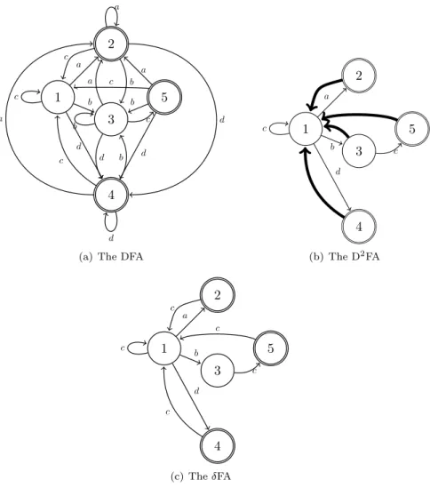
2.1 Automata recognizing (a+),(b+c) and (c∗d+). . . 41
2.2 δFA internals: a lookup example. . . 45
2.3 Automata recognizing .*ab[ˆa]*c and .*def . . . 46
2.4 Distribution of the number of bits used for a relative identifier with our compression scheme for standard rule sets. . . 48
2.5 Mean number of memory accesses for δFA, BEC-CRO and D2FA for different datasets. . . 52
2.6 Comparison of speed performance and space requirements for the dif-ferent algorithms. . . 53
2.7 Automata recognizing (a+), (b+c) and (c∗d+). . . . 55
2.8 δ2FA internals: a lookup example. . . 56
2.9 Schematic view of the problem. Same color means same properties. If the properties of S3 are set temporary, the ones in S1can be avoided. 57
2.10 Mean number of memory accesses. . . 60
2.11 A very simple DFA . . . 62
2.12 An example of Co-occurrence Permutation for 3-bit characters . . . . 65
2.13 Ratio of transitions stored when Co-occurrence Permutation is used compared with the minimum number of transitions. The ratio is com-puted with respect to the case when no permutation is adopted. . . . 66
2.14 An example of state construction in h-DFA for 3-bit characters. The numbers on the leaves are pointers to next states . . . 66
2.15 Mean number of memory accesses per character. . . 69
2.16 Examples of sampling with θ = 2. The regex to match is ab. ∗ cd, the sampled one is [ab].∗[cd] and the text consists of 16 bytes. Arrows point to observed chars. Sampling performs 12 memory accesses in case of a real match(b) or false alarm(c) or even 8 in the average non-matching case(a). In (c) the striked arrow point to the non-matching char. . . . 71
2.17 Example of the finite automata needed for sampling (only the forward transitions are shown for readability): (a) is the standard DFA, (b) is the sampled one (with θ = 2) and (c) is the reverse DFA. . . 76
2.18 Example of a sampled DFA for regular expression: abc ∗ d. Only some edges are shown. . . 78
2.19 Using an overall reverse DFA (one) or one DFA per regex subset (all). 80 2.20 Bit rate with a standard DFA (θ = 1) and sampled DFAs (θ = 2, 3, 4). 82 2.21 Bit rate with k-DF A and our DF As. . . . . 82
2.22 False alarms, length and range for each signature. . . 83
2.23 Addition of a new string in a CBF. . . 86
2.24 The scheme of our system. . . 88
2.25 The string is SIGNATURE. The piece SI is not outright detected, and when the piece GNA generates an alert, it has already been processed. 90 2.26 Detection percentage and false positives by varying α. . . 92
3.1 Example of hash retrieval by using OBT and HSBF. . . 98
3.2 Example of hash retrieval in the optimized structure. . . 99
3.3 The desired data structure . . . 104
3.4 Probability of good BFs as a function of α and k. . . 105
3.5 Overall scheme. Here the parameters ε = 2 and m = 16 are quite over-dimensioned in order to better illustrate the idea. . . 106
3.6 The bipartite matching problem. . . 107
3.7 Minimal m for the construction of iBF . . . 109
3.8 Ratio of m over minimal m for the construction of iBF . . . 109
3.9 Number of bits per element m/n. . . 109
3.10 False positives in a iBF for n = 100, 400, 1000, 2000. . . 110
4.1 Distribution of prefix values belonging to different forwarding tables. . 115
4.2 Example of lookup by using RLA and then Lulea or Tree Bitmap. . . 117
4.3 First step: the choice of the parameter b. . . 118
LIST OF FIGURES
4.4 Variation of memory consumption and mean number of memory ac-cesses of the RLA algorithm with respect to α for the database of 2006.120
4.5 A picture of the different structures used in our lookup scheme. . . 124
4.6 Flow diagram of H-cube lookup process. . . 126
4.7 Memory consumption for the different lookup schemes. . . 129
4.8 Memory occupancy versus number of accesses. . . 129
4.9 The overall IP lookup scheme. . . 131
4.10 BT-array schematic. . . 131
4.11 Mean bit-rate achieved with different forwarding tables. . . 134
4.12 Structure of the classifier. . . 138
4.13 Structure of the classifier. . . 138
4.14 Structure of the classifier. . . 139
4.15 Throughtput of the classifier with constant-rate traffic of interest and different rates of the background traffic (ρ stands for link utilization). 140 4.16 Throughtput of the classifier with growing rates of the traffic of interest.141 5.1 The overall monitoring scheme. . . 145
5.2 The Timestamp and Packet data streaming are passed in parallel. . . 146
5.3 Flow Diagram of the Core Monitoring. . . 148
5.4 Format of the Packet sent to the CPU. . . 149
5.5 System setup. . . 150
5.6 Comparison of the two absolute drift with the naive timestamping mod-ule. . . 151
5.7 Comparison between the two oscillator with the naive timestamping module. . . 151
5.8 Architecture of BRUTE. . . 153
5.9 Architecture of BRUNO. . . 155
5.10 Structure of a packet request (PR). . . 156
5.11 A flow structure. . . 157
5.12 Address Translation. . . 159
5.13 DRAM window circular buffer. . . 160
5.14 Schematic view of BRUNO as a system . . . 163
5.15 Energy of the impulse response of G(z). . . 164
5.16 Estimated Power Spectral Density of ω(n). . . 165
5.17 Square absolute frequency response of G(z). . . 165
5.18 CBR traffic: Brute vs Bruno. . . 166
5.19 Bar chart of interarrival times of a Poisson traffic (λ = 0.03). . . 168
5.20 PAB traffic profile. . . 169
5.21 Variance time of generated PAB traffic. . . 169
5.22 Interarrival times of a 40s SIP call. . . 170
List of Tables
1.1 Units and functionalities of Agere system. . . 12
1.2 Processors and functionalities of RSP unit. . . 12
1.3 Processors of NP-1. . . 21
1.4 Co-processors of IBM NP. . . 22
1.5 Properties of IXP2400 memories. . . 29
2.1 Percentage of states reached by edges with the same one label (p1char), C-S compression (rcomp), average number of scratchpad accesses per lookup (ηacc) and indirection-table size (TS). . . 47
2.2 Characteristics of the rule sets used for evaluation. . . 49
2.3 Compression of the different algorithms in terms of transitions and memory. . . 51
2.4 Number of transitions and memory compression by applying δFA+C-S to XFA. . . 53
2.5 Simple vs. Optimal approach: ratio of deleted and temporary transitions. 59 2.6 Compression of the different algorithms. In (b) the results for δFA and δ2FA include char-state compression. . . . 59
2.7 Compression of the different 1-step algorithms in terms of transitions and memory. . . 68
2.8 Memory and transition compression (%) for 2 and 3-step h-DFA + Char-State compression . . . 69
2.9 Performance of the standard system in terms of detected attacks and false positives. . . 91
2.10 The effects of deleting the most frequent substrings. . . 92
3.1 Memory requirements in bits/key. . . 100
3.2 Algorithm comparison. . . 101
3.3 Terms and notation used through the work . . . 103
4.1 Average prefix length distribution for IPv4 BGP table. . . 115
4.2 Performance of RLA and memory gain with respect to multibit trie and direct addressing. . . 118
4.3 Performance of RLA compared to Lulea and Tree Bitmap. . . 121
4.4 Construction time and memory consumption for our scheme. . . 127
4.5 The cost of H-cube lookup in terms of memory accesses. . . 128
4.6 Resource utilization for the original lookup algorithm. . . 133
4.7 Utilization for our algorithm. . . 133
4.8 Utilization for our overall project. . . 133
5.1 Device utilization for the Passive Monitoring System. . . 149
5.2 Mean times for each operation in clock cycles. . . 162
5.3 Interdeparture time variation reduction achieved by the correction mech-anism. . . 171
Introduction
The amount of Internet traffic and link bandwidth increase day by day, and this forces network devices to meet harder and harder requirements.
The growth of users and applications pushes researchers towards the development of novel and audacious ideas and modern and fast devices. The rise in links capacity reduces the time available to network devices for packet processing (for instance, on a gigabit link a packet has to be processed within about 0.7 µs). A simple solution is, of course, the adoption of massive parallelism. However, increasing the number of processing engines is an expensive approach and increases the memory bandwidth requirements. For these reasons, tasks like Packet Classification and Deep Packet In-spection are still a critical processing for network devices, thus permanently requiring improvements and new algorithmic solutions. Several solutions for these problems are described in this work; all of them take into account real applications and development in high performance platforms such as NetFPGA and Network Processors. The first chapter of the thesis introduces NetFPGA and Network Processors with greater at-tention to Intel ones which have been adopted in many of the works described herein. With chapter 2, we move into Deep Packet Inspection, by discussing solutions based on DFA and Bloom Filters. Then, chapter 3 introduces two novel perfect hashing schemes, which are useful in devices provided by a limited amount of memory. They are based on randomized techniques and show remarkable results. Chapter 4 de-scribes IP-lookup and Packet Classification techniques based on heuristic, hash tables and DFA (Deterministic Finite Automata). Finally chapter 5 describes two ideas for low-cost IP Traffic Generation ad Monitoring at high-speed.
Chapter 1
Introduction to FPGA-based
Networking Boards and
Network Processors
In this chapter we introduce FPGA-based networking boards and Network Processors. The most popular of the former, NetFPGA [1] and Combo series [2], are presented with greater attention to the NetFPGA which have been adopted in many of the works described herein. Only a brief introduction of Combo6, for the Combo series is inserted. We introduce also a comparison among Network Processor Platforms with greater interest in Intel ones, used extensively in the works presented herein. NetFPGA and Intel Network Processor have always been taken as reference in the design and development of the proposed algorithms in this thesis.
1.1
FPGA-Based Networking Boards
The main idea of the FPGA-based cards like NetFPGA and Combo6 is to give de-velopers a possibility to work with “open hardware” and use it in the same way as open-source software. The heart of these cards consists of one or more FPGA (Field Programmable Gate Array) chips, memories and other necessary components (power supply, IO chips, connectors etc.). Due to the flexibility of FPGA chips, the func-tionality of these cards can be easily (and quickly - within just several milliseconds) changed by loading a new design into the FPGA. This approach can be used for many different research and development projects.
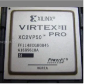
Figure 1.1: The NetFPGA main core: a Xilinx Virtex II Pro FPGA.
1.1.1
What is an FPGA?
An FPGA (Field Programmable Gate Array) is a software programmable digital de-vice. Field–Programmable means that the customer can configure it after manifac-turing. FPGAs are usually a good trade-off between ASICs (Application Specific In-tegrated Circuit) and PAL (Programmable Array LOgic). FPGA offer the advantage of obtaining the same functions that an ASIC could perform while being amenable to modifications even after the chip is deployed in a product.
FPGAs are used in a great variety of applications like communications, automotive, consumer, etc. The designer can program them directly, achieving:
• a reduction of the project time
• a direct verify making use of simulations • trails on the application field
A functionality error can be simply corrected by re–programming the device and the design environments are largely user–friendly. These are the reasons why FPGAs are usually preferred to ASICs in the project phase, while their high price and large power consumption are unconvenient for large–scale prodution. So this is the formula which is rapidly growing: FPGAs for experimentations and designing, and ASICs for productions.
1.1.2
FPGA Design and Programming
FPGAs are programmed with Hardware Description Languages (HDL) like Verilog or VHDL, or making use of a “schematic–entry” mode that can offer a fast and sim-plified approach with the same performances. Leader companies such as Xilinx and Altera give a complete development environment to support their entire product-line, so customer can just create their own application, simulate it and then download it to the FPGA platform to verify its functionality. Using an electronic design automa-tion tool, a technology-mapped netlist is generated. The netlist can then be fitted to the actual FPGA architecture using a process called place–and–route, usually per-formed by the FPGA company proprietary place-and-route software. The user will validate the map, place and route results via timing analysis, simulation, and other verification methodologies. Once the design and validation process is complete, the
1.1 FPGA-Based Networking Boards
binary file generated (also using the FPGA company’s proprietary software) is used to (re)configure the FPGA.
Figure 1.2: FPGA design flow.
The most common HDLs are VHDL and Verilog, although in an attempt to reduce the complexity of designing in HDLs, which have been compared to the equivalent of assembly languages, there are attempts to raise the abstraction level through the introduction of alternative languages. In a typical design flow, an FPGA application developer simulates the design in multiple stages throughout the design process. Ini-tially the RTL description in VHDL or Verilog is simulated by creating test benches to simulate the system and observe results. Then, after the synthesis engine maps the design to a netlist, the netlist is translated to a gate level description where simulation is repeated to confirm the synthesis reports no errors. Finally the design is laid out in the FPGA at which point propagation delays can be added and the simulation run again with these values back-annotated onto the netlist. As it can be seen, design verification, which includes both functional verification and timing verification, takes places at different stages during the design flow, giving the designer the chance to verify step by step his project without wasting time.
1.1.3
The Combo6
Figure 1.3: Combo6 upright view.
Combo6 developed in the Liberouter project [3] by CESNET in cooperation with the Faculty of Information Technology in Brno is a PCI card primarily dedicated for a dual-stack (IPv4 and IPv6) router hardware accelerator. It can be used in
applications either alone (as a hardware coprocessor) or with add-on cards as an accelerated interface PCI card. It consists of Xilinx Virtex II FPGA, 2Mb TCAM, 256MB DRAM and 6Mb SSRAM. Various add-on cards can be used with Combo6 card. Add-on SFP card with 4 GE interfaces and 2 Virtex II FPGAs is an example of one of the Combo6 interface cards. The communication between interface and Combo6 card is realized via 100-bits wide 3-state bus with maximal clock frequency of 153MHz (maximal DDR transfer rate is approx. 3,8GB/s). Unfortunately the interconnection connector between Combo6 and its interface card is often source of reliability problems.
1.1.4
The NetFPGA
The NetFPGA platform has been developed in Stanford University by the High Per-formance Networking Group as an open platform available to developers worldwide. It is a reusable networking hardware with a simple modular design based on a low– cost FPGA platform. Its primary goal is to give students, teachers and researchers a fast and powerful tool to experiment new ways to process packets at line–rate. A set of reference designs is provided with the NetFPGA board, such as an IPv4 Router or a simple Network Interface Card. Several developers all over the world are using the platform to build advanced network flow processing systems.
Figure 1.4: NetFPGA upright view.
1.1.4.1 Architecture
NetFPGA is a PCI card that plugs into a standard PC. As main components, the card contains an FPGA, four 1GigE ports and some buffer memory (SRAM and DRAM). A block diagram that presents the major components of NetFPGA platform is shown in figure1.5. This platform contains one Xilinx Virtex2–Pro 50 FPGA which is pro-grammed with user–defined logic and has a core clock that runs at 125M hz. The NetFPGA platform also contains one small Spartan II FPGA holding the control logic for the PCI interface to the host processor.
Two 18M Bit external Cypress SRAMs are arranged in a configuration of 512k words of 36bits (4.5M bytes total) and operate synchronously with the FPGA logic at 125M Hz. One bank of external Micron DDR2 SDRAM is arranged in a configuration of 16M words of 32bits (64M Bytes total). Using both edges of a separate 200M Hz clock, the memory has a bandwidth of 400M W ords/second (1, 600M Bytes/s = 12, 800M bits/s).
1.1 FPGA-Based Networking Boards
Figure 1.5: NetFPGA Block Diagram.
The Broadcom Gigabit/second external physical-layer transceiver (PHY) sends pack-ets over standard category 5, 5e, or 6 twisted-pair cables. The quad PHY inter-faces with four Gigabit Ethernet Media Access Controllers (MACs) instantiated as a soft core on the FPGA. The NetFPGA also includes two interfaces with Serial ATA (SATA) connectors that enable multiple NetFPGA boards in a system to exchange traffic directly without use of the PCI bus.
1.1.4.2 Reference Pipeline Details
Figure1.6shows the reference pipeline. The NetFPGA adopts the common approach of networking hardware which is generally arranged as a pipeline through which pack-ets flow and are processed at each stage. Stages are interconnected using two point– to–point buses: the packet bus and the register bus.
The packet bus transfers packets from one stage to the next using a synchronous FIFO packet-based push interface, over a 64–bit wide bus running at 125Mhz (an aggregate rate of 8Gps). In this scenario, stage i pushes data forward when the next stage has space for a packet word (i.e.: the FIFO is not full). The FIFO interface has the advantage of hiding all the internals of the module behind a few signals and allows modules to be concatenated in any order. It is the simplest interface can be used to transfer information and provide flow control while still being sufficiently efficient to run designs at full line–rate.
The first stage in the pipeline consists of several queues (Rx queues). These queues receive packets from IO ports such as the Ethernet ports and the PCI over DMA and provide a unified interface to the rest of the system. These ports are connected into a wrapper called the User Data Path which contains the processing stages. The cur-rent design has 4 Ethernet Rx queues and 4 CPU DMA queues. Packets that arrive into CPU DMA Rx Queue X are packets that have been sent by the software out of interface nf2cX. In the User Data Path, the first module a packet passes through is the Input Arbiter. The input arbiter decides which Rx queue to service next, and pulls the packet from that Rx queue and hands it to the next module in the pipeline: The output port lookup module. The output port lookup module is responsible for
Figure 1.6: The Reference Pipeline.
deciding which port a packet goes out of. After that decision is made, the packet is then handed to the output queues module which stores the packet in the output queues corresponding to the output port until the Tx queue is ready to accept the packet for transmission. The Tx queues are analogous to the Rx queues and they send packets out of the IO ports instead of receiving. Packets that are handed to DMA Tx queue X pop out of interface nf2cX.
1.1.4.3 Life of the Packet
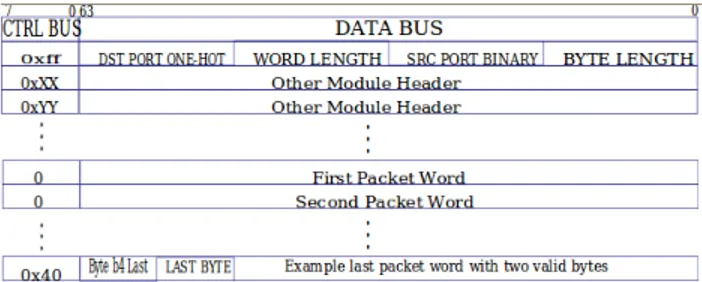
Packets enters and exit the pipeline through various Receive and Transmit Queue modules respectively. To keep things simple, the interface is packet–based. Modules are not required to process multiple packets at a time, and they are not required to split the packet header from its data (altough a module is free to chose to do so internally). As the packet moves from one stage to the next, a stage can modify the packet itself and/or parse the packet to obtain information that is needed by a later stage for additional processing on the packet. This extracted information is prepended to the beginning of the packet as a 64–bit word which is called module header and is uniquely identified by its ctrl word from other module headers. Subsequent stages in the pipeline can identify this module header from its ctrl word and use the header to perform additional processing on the packet. The ctrl world is non-zero for module headers and distinguishes module headers from each other when there are multiple module headers. When the actual packet received starts after the module headers, the ctrl word is reset to 0, and then at the last word of the packet, the ctrl lines will indicate which byte is the last byte in the last word. The Rx Queues create a module header when they receive a packet and prepend it to the beginning of the packet. The Rx queues store the length of the packet in bytes at the lowest 16bits of the module header, the source port and the packet length. The Input Arbiter selects an Rx queue to service and pushes a packet into the Output Port Lookup module. The Output Port Lookup module decides which output port(s) a packet goes out of and writes the output ports selection into the module header. The Output Queues module
1.1 FPGA-Based Networking Boards
Figure 1.7: Format of the packet passing on the packet bus.
Figure 1.8: Register access system.
looks at the module header to decide which output queue to store the packet in and uses the lengths from the module header to store the packet efficiently. After the packet is removed from its output queue and pushed into its destination Tx Queue, the module header is finally removed before sending the packet out of the appropriate port. Packets on the packet bus are formatted as shown in figure1.7.
1.1.4.4 Register Pipeline
The register bus provides another channel of communication that does not consume Packet Bus bandwidth. It allows information to travel in both directions through the pipeline, but has a much lower bandwidth. A common register interface, done by memory–mapping, make the hardware registers, counters and tables visible and con-trollable by software. The memory–mapped registers, in turn, appear as I/O registers to the user software that can access them using ioctl calls.
The register bus strings togheter register modules in each stage in a pipeline daisy– chain that is looped back in a ring. One module in the chain initiates and responds to requests that arrive as PCI register requests on behalf of the software. However, any stage of the chain is allowed to issue register access requests, allowing information to trickle backwards in the pipeline, and allowing stage i to get information from stage i + k. This daisy–chain architecture is preferable to a centralized arbiter
ap-Figure 1.9: Architecture of NP Agere.
proach because it facilitates the interconnection of stages while limiting inter–stage dependencies. Figure1.8shows this register bus architecture.
1.2
Comparison among Network Processor Platforms
Nowadays no official standard for network processors yet exists. Each vendor has proposed its specific solution. The common features of all proposals are a hierarchy of processors, a series of memory devices with different sizes and latencies, a low-level programmability. The target is a platform for networking applications with low time to market and high time in market, thanks to a high flexibility and a easy programmability. In this section, we first present a comparison among the available network processor platforms and then a detailed description of the hardware reference of our activity, the Intel IXP2XXX family.
1.2.1
Multi-chip Pipeline (Agere)
Agere System Incorporated (i.e. the microelectronics branch of Lucent Technologies) presents a NP family called Payload Plus [4]. It has three interesting features: a multichip architecture, a programmable classifier, a flexible management of input data.
1.2.1.1 Architecture
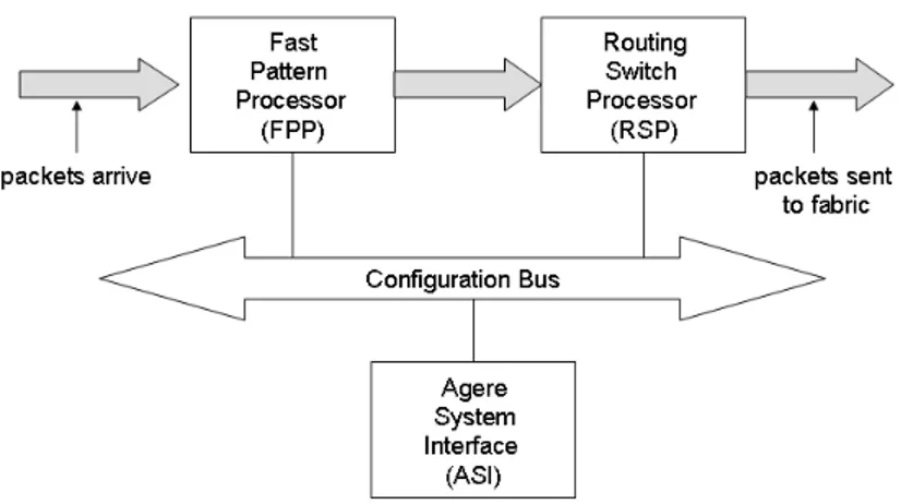
The Agere system is composed by three different units. Fig. 1.9shows the intercon-nections among the different chips and the data flow through the consequent pipeline. The Fast Pattern Processor (FPP) and the Routing Switch Processor (RSP) establish the basic pipeline for fast data path processing. The ingress packets are forwarded to the FPP, which sends them, along with an instruction set, to the RSP. The packets
1.2 Comparison among Network Processor Platforms
Figure 1.10: Internal structure of FPP unit.
are then forwarded toward the switching fabric. A third chip, the Agere System In-terface (ASI) is a co-processor that introduces new functionalities to improve general performance. The ASI gathers statistical information on packets, which are then used for traffic management. Moreover the ASI provides a connection toward a distinct processor (not shown in figure), which is used to manage the overall system and the exception packets.
The system offers other connections: for instance, the configuration bus connects also the ingress hardware interfaces in order to coordinate the data flow toward the FPP. Fig. 1.10shows the internal architecture of the FPP.
1.2.1.2 Processors and functional units
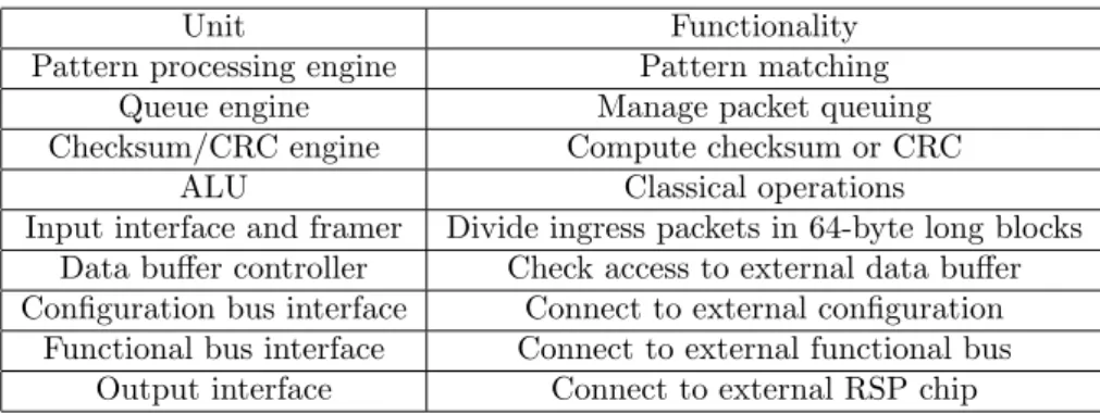
Each chip in the Agere system contains several processors and provides different func-tionalities. Tab1.1shows the features of each component. The Functional Bus Inter-face (FBI) implements an interesting form of Remote Procedure Call (RPC), which allows for calling functions which are external to the FPP unit. This way it is possible to extend the FPP functionalities by adding ASIC hardware.
Moreover, the FPP contains the interfaces for each external connection. For instance, the pattern processing engine can interface to an external control memory by means of a program memory and a queue engine. To handle packets, the FPP has an ingress interface, a framer that divides packets in 64 bit long blocks and an output interface for the configuration bus. The FPP contains also an external interface for the configuration bus. The central part is given by a functional bus, which all the processors can connect to. There is also an external interface for the functional bus
Table 1.1: Units and functionalities of Agere system.
Unit Functionality
Pattern processing engine Pattern matching
Queue engine Manage packet queuing
Checksum/CRC engine Compute checksum or CRC
ALU Classical operations
Input interface and framer Divide ingress packets in 64-byte long blocks Data buffer controller Check access to external data buffer Configuration bus interface Connect to external configuration
Functional bus interface Connect to external functional bus Output interface Connect to external RSP chip
Table 1.2: Processors and functionalities of RSP unit.
Unit Functionality
Stream editor engine Packet modification
Traffic manager engine Regulate traffic and hold statistics Traffic shaper engine Check QoS parameters
Input interface Receive packets to FPP
Packet assembler Store arriving packets
Queue manager logic Interface to external traffic scheduler Output interface External connection for output packets Configuration bus interface Connect to external configuration bus
which is used by the ASI for checking the processing. The RSP unit, whom internal structure is shown in 1.11, has a set of processors and functionalities listed in tab.
1.2. The stream editor, the traffic manager and the traffic shaper have been built with Very Long Instruction Word (VLIW) processors.
1.2.1.3 Memory
In the Agere architecture, both external and internal memory are provided. The FPP divides packets in blocks and stores them in an external data-buffer (by means of an interface on the chip). It uses the internal memory for packets in the processing stage, while the external memory is used to store programs and instructions. The RSP stores packets in an external SDRAM and uses a Synchronous Static RAM (SSRAM) for high priority queues.
1.2.1.4 Programming support
Ease programming is an appealing feature of Agere chip. The FPP is a pipelined multithreaded processor and provides 64 independent contexts. However the paral-lelism is hidden to the programmer, who is able this way to use high-level languages.
1.2 Comparison among Network Processor Platforms
Figure 1.12: The Alchemy chip.
Agere offers also a specific language for the classification, a Functional Programming Language (FLP), and a scripting language, the ASL (Agere Scripting Language). Moreover, Agere offer a substantive support for traffic management. The logic of RSP allows for using multiple queues, applying external scheduling rules and han-dling traffic shaping.
1.2.2
Augmented RISC Processor (Alchemy)
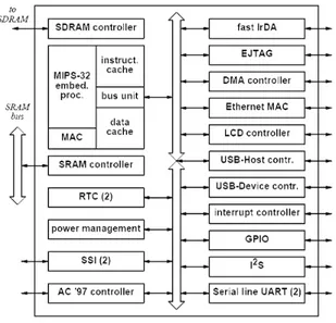
Alchemy semiconductors Inc. (acquired by Advanced Micro Devices) offers different versions of Network Processors with different speeds [5]. These solutions are based on a RISC processor which is enriched by instructions specialized on packets processing.
1.2.2.1 Architecture
This architecture is characterized by an embedded RISC processor along with a series of co-processors. The core, a CPU MIPS-32, uses a 5-stages pipeline, the pipelined register file access and the zero penalty branching to improve the performance. Many instructions have been added to the set, such as a “multiply and accumulate” to aid in CRC or checksum computing. Other added instructions are those for memory prefetch, for conditional move operations, count leading of 0s and 1s. Fig. 1.12shows the internal organization of Alchemy chip.
1.2.2.2 Processors and functional units
As shown in fig. 1.12, the embedded RISC processor can access to a certain number of I/O controllers and functional units. The chip contains also an RTC (Real Time Clock) unit.
1.2 Comparison among Network Processor Platforms
1.2.2.3 Memory
On the chip there are two caches of 26KB, one for instructions and one for data, and connections for external SDRAM e SSRAM. The bus which connects the SSRAM provides also access to a Flash Memory, a ROM and a PCMCIA unit.
1.2.2.4 Programming support
Given that the Alchemy chip uses a MIPS processor, it can be programmed in C language.
1.2.3
Embedded Processor Plus Coprocessors (AMCC)
Applied Micro Circuit Corporation (AMCC) offers a series of NPs with different performance [6]. The AMCC architecture allows for efficiently using parallelism in order to obtain high data-rates.
1.2.3.1 Architecture
The version nP7510 includes 6 embedded processors (called nP cores), which work in parallel (e.g., a packet transform engine, a policy engine, a metering engine) and other functional units which provide external interfaces. An external co-processor handles address lookups based on a Longest Prefix Match algorithm. Fig. 1.13 shows the scheme of AMCC chip.
1.2.3.2 Processors and functional units
Each processor provides hardware threads at zero context switch. This way, the nP7510 can simultaneously process more packets or cells. The programming model of AMCC allows for hiding the parallelism to programmer, who can write code as for a single processor. Moreover, each packet or cell is processed by a single thread, this way avoiding to partition the code and implement complex balancing algorithms. The Packet Transform Engine, which is optimized for packets or cells, allows for operations on frames in parallel with the nP cores; several operations can be made in a single instruction: insert or delete data, compute and add the CRC or change values in packet header. The Special Purpose Engine enables the elimination of mutexes or other software threats for synchronizing access of thread to shared resources. The Policy Engine is dedicated to search and classification operations. Many lookups (up to 512 with compound keys) can be simultaneously made with a fixed latency. A key feature of Policy Engine is the “Network-Aware CASE Statement”: the use of multiple and concurrent classifications allows for the elimination of nested “if-then-else” instructions, this way reducing code and improving performance. The metering engine enables the collection of information for the remote monitoring of SNMP, while the Statistic Engine enables the automated collection of statistics based on RMON protocol. The nP7510 has been designed to support a speed of 10 Gbps. It can be interfaced with the traffic management chipset nPX5710/20. The configuration can be doubled in order to handle a full duplex traffic of 10 Gbps. The nPX5710/20 contains also a virtual SAR unit (Segmentation And Reassembly).
1.2.3.3 Memory
As for many NPs, the AMCC chip offers external and internal memories. Moreover, a controller manages the two types of memory and hides this double nature to processor. An external TCAM is used for packet classification processes.
1.2.3.4 Programming support
These processors can be programmed in C or C++; AMCC provides a compiler, an assembler and a debugger.
1.2.4
Pipeline of Homogeneous Processors (Cisco)
The Parallel eXpress Forwarding (PXF) network processor has been designed by Cisco to be used in Cisco routers [7].
1.2.4.1 Architecture
The PXF adopts a parallel architecture that can be configured in order to create a series of pipelines. A single chip contains 16 embedded processors that can be put to work on 4 parallel pipelines. Figure1.14shows a possible organization of processors.
1.2 Comparison among Network Processor Platforms
Figure 1.14: A possible configuration of CISCO XPF.
1.2.4.2 Processors and functional units
The PXF architecture counts a separation between control plane and forwarding plane. A route processor cares of routing protocols, network configuration, errors handling, and packets which are destined to the router. Instead, the forwarding plane is controlled by the PXF technology. In the PXF, each processor is optimized for packet processing at high speed and it is completely independent of the other ones; these units are called Express Micro Controllers (XMCs) and contain a complex dou-ble execution unit, provided with several specific instructions for an efficient packet processing. Moreover the XMCs can access to different resources on the chip, as reg-ister files and timers. They have also a shared access to an external memory in order to store state information, such as routing tables and packet queues. Finally, some micro-controllers guarantee that processing results can be passed among subsequent XMCs on the same pipeline. Figure 1.15 illustrates the path of a packet through this architecture. In this configuration, 2 PXF network processors are used for each Performance Routing Engine (PRE), this way obtaining 4 pipelines of 8 processors. Whenever a packet goes to a PRE from the ingress interface, it enters the ASIC back-plane interface and is bufferized in the input packet memory. The header is extracted and sent to PXF for packet classification, header modification and, if needed, data modification. The processing comprehends also the selection of the port on which packet forwarding is performed. By means of simple routine algorithms, the PXF instructs ASIC backplane interface to store packet in its packet-buffer memory, in one of the possible queues which are associated to corresponding output queues. Then, the scheduling function of PXF processes this queue in order to determine what is the next packet to be forwarded. After this decision, the PXF instructs ASIC backplane interface to copy this packet in the hardware queue associated to corresponding egress interface.
Figure 1.15: Standard path of a packet in a PRE.
1.2.4.3 Memory
There is an independent memory for each processor and one for each column of pro-cessors, in order to optimize accesses.
1.2.4.4 Programming support
This network processor is realized for internal use, and not as general-purpose product, thus it uses private software. Microcode and Cisco IOS are combined to provide processing functions. The association of these functions to the processors pipeline is very flexible and can be updated when new functions are available to be added.
1.2.5
Configurable Instruction Set (Cognigine)
The network processor of Cognigine Corporation is an example of reconfigurable logic: the adopted processor has not a prefixed set of instructions.
1.2.5.1 Architecture
This architecture allows for using up to 16 processors, which can be interconnected to form a pipeline. Each processor is called Reconfigurable Communication Unit (RCU) and has a connector that links it to RSF (Routing Switch Fabric), this way allowing for communications arbitrage and planning. The RCUs are connected in a hierarchical manner: a crossbar is used to connect a group of 4 RCUs and another one to connect groups of RCUs. This solution allows for scaling the architecture for a big number of RCUs. The RSF permits to divide a transaction in order to hide latencies; it is accessed by a RCU through a memory mapping. Each RCU contains 4 execution
1.2 Comparison among Network Processor Platforms
Figure 1.16: Internal structure of Cognigine network processor.
units which can be dynamically reconfigured. Each unit uses an instruction set called Variable Instruction Set Communications (VISC). As for a standard processor, a VISC instruction performs an easy operation, but details of operation are not determined a priori. In fact, the chip contains a dictionary which defines the interpretation of each instruction: operands’ size, how they can be employed, the basic operation and the predicate. The dictionary is in turn configurable, elements can be added or dynamically changed. This way, programmer can define a personal instruction set, insert the interpretation of these instructions and develop a program based on them. For instance, a programmer could define an instruction set optimized for peculiar processings or specific protocols. VISC instructions are decoded during the first stage of the pipeline. Each RCU provides a five-stage pipeline and hardware support for 4 threads. The interconnections among processors are again configurable. For each RCU there are 4 64-bit data buses and 4 buses at 32-bit addresses, which allows for connecting RCUs in pipeline.
1.2.5.2 Memory
RCUs access to different types of memory, such as the internal SSRAM or the Double Data Rate SDRAM (DDR-SDRAM). Dictionary for VISC instructions is allotted in a distinct memory. Memories compose a hierarchy where the fastest ones are internal registers and scratchpad memory, then the cache for instructions and memory dedicated to data, while the slowest ones is the external memory, which is designed to store packets.
Figure 1.17: The scheme of NP-1 chip.
1.2.5.3 Programming support
In order to maximize the parallelism, the RCUs provide hardware support for multi-threading. Moreover, there are connections to external buses, as the PCI bus. Finally, along with C compiler and assembler, Cognigine offers a support for a classification language.
1.2.6
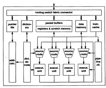
Pipeline of heterogeneous processors (EZchip)
EZchip Corporation produces the network processor NP-1 [8]. This architecture shows as heterogeneous processors, each of them dedicated to specific functions, can work together in a pipeline manner. The NP-1 has been designed for a big target: processing of layers 2-7 at 10 Gbps. This chip contains also a very fast SRAM, which is used for storing packets and lookup tables. There is an interface to access an external DRAM (external SRAMs and CAMs are not necessary). The chip includes also an interface for an external processor for management and control functions (the interface is not shown in figure). Moreover, EZchip claims to use patented algorithms which allows embedded memory for searching in external memories, in order to support a line-rate of 10 Gbps. These algorithms and the associated data structures allow for searches with strings of variable length. Further details are not publicly available.
1.2.6.1 Architecture
In this chip there are the Task Optimized Processors (TOPs). Each TOP has a personal set of instructions and connections which is specific for the functionalities that it must provide. Figure1.17illustrates chip architecture.
1.2 Comparison among Network Processor Platforms
Table 1.3: Processors of NP-1.
Processor type Optimized for
TOPparse Header field extraction and classification
TOPsearch Table lookup
TOPresolve Queue management and forwarding TOPmodify Header and payload modification
Figure 1.18: Internal architecture of IBM network processor.
1.2.7
Extensive and Diverse Processors (IBM)
IBM produces a family of network processors called PowerNP [9]. This solution is very complex and comprehends a wide gamma of processors, co-processors and functional units.
1.2.7.1 Architecture
This network processor contains programmable processors and several co-processors which handle searches, frame forwarding, filtering and frame modification. The ar-chitecture is composed by a set of central embedded processors, along with many supporting units. Fig. 1.18shows the overall architecture, while fig. 1.19accurately illustrates the area called Embedded Processor Complex (EPC).
In addition to the embedded PowerPC, the EPC contains 16 programmable processors, which are called picoengines. Each picoengine is multithreaded, thus improving again performance. In order to speed up processing, frames are processed before being passed to the protocol processor in the EPC. The ingress physical MAC multiplexor
Figure 1.19: The EPC chip in the IBM NP.
Table 1.4: Co-processors of IBM NP.
Co-processor Function
Data Store Frame buffer DMA
Checksum Compute and check header checksums
Enqueue Forward frames arriving from switch or target queues Interface Provide access to internal registers and memory String Copy Transfer big amounts of data at high speed
Counter Update counters used in protocol processing
Policy Handle traffic
1.2 Comparison among Network Processor Platforms
takes frames arriving from physical interface, checks CRC and passes frames to ingress data store. The first part of frame, which contains headers up to layer 4, is passed to the protocol processors, while the remaining part is stored in memory. Once frame has been elaborated, the ingress switch interface forwards it toward the proper output processor through the switching fabric. The external hardware of the EPC takes care also of the output of frames. The egress switch interface receives data from the switching fabric and stores them in the egress data store. The egress physical MAC multiplexor handles frame transmission, by extracting them from egress data store and sending them to physical interface. In addition to picoengines, the chip of IBM contains several co-processors specialized for particular functions. Some examples are presented in table1.4.
1.2.7.2 Memory
The PowerNP provides access to an external DDR-SDRAM and presents many in-ternal memories, with an arbiter which coordinates accesses to them. The inin-ternal SRAM provides fast access, which allows for temporarily storing packets to be pro-cessed. Moreover, programmable processors have a dedicated instruction memory; for instance, each picoengine has 128 KB of private memory which is dedicated to this purpose.
1.2.7.3 Programming support
In addition to standard programming tool (such as compilers, assemblers, etc.), the IBM chip provides a software package for simulation and debugging. This package is available for several operative systems, such as Solaris, Linux and Windows. The co-processor that cares about traffic management works at wire speed, this way the IBM chip is able to analyze each packet in order to verify that traffic is complying to predetermined parameters.
1.2.8
Flexible RISC Plus Coprocessors (Motorola)
The Motorola Corporation brands its network processors C-Port. Models C-5, C-5e and C-3 represent a tradeoff between performance and power consumption.
1.2.8.1 Architecture
The Motorola chip is very appealing; it is an example of internal processors which can be configured to work in a parallel or pipeline manner. The capability of selecting a configuration model for each processor provides a high flexibility to C-Port. Fig.
1.20 shows as C-Ports can connect more physical interfaces to a switching fabric. Each network processor includes 16 blocks of processors, which are called Channel Processors and care for packet processing. Each CP can be configured in different ways. The most direct approach is the dedicated configuration, which establishes a one-to-one relation between the CP and the physical interface. In this configuration the Channel Processor must manage both the input and the output, and is suitable for interfaces at medium or low speed (100Base-T Ethernet or OC-3), for which the processor has enough power. In order to handle higher speeds, the Channel Processors
Figure 1.20: Architecture of C-Port.
can be organized in a cluster in a parallel way. This way, whenever a packet arrives, any CP in idle state can handle such a packet. The number of CPs in each cluster can be modified, thus the designer can select the proper sizes according to the interface speeds and the amount of required processing. Figure 1.20 shows chip C-Port C-5 architecture, where CPs are configured in cluster. The diagram illustrates the 16 Channel Processors (CP − 0 . . . CP − 15) configured in parallel clusters of 4 CPs per cluster. In addition to CPs, the Motorola chip contains many other co-processors. The Executive Processor provides a configuration and management service of the overall Network Processor; it communicates with a potential host PC via bus PCI or through serial lines. The Fabric processor allows for a fast connection between the internal buses and an external switching fabric. The lookup unit allows for speeding up searches in lookup tables. The buffer management and queue management units handle and check respectively buffers for packets and queues. However, the name Channel Processor is misleading: the chip does not contains an only processor, but is a complex structure with a RISC processor and several functional units which aid in handling packets at high speed. Fig. 1.21 shows CP components and their interconnections. As we see, the CP has a parallel structure for ingress and egress side. The Serial Data Processor (SDP) is programmable and on the ingress side cares for checking checksum or CRC, decoding, analyzing headers, while on the egress side is used for modifying frames, computing checksum or CRC, coding, and framing. The RISC processor deals with classification processes, traffic handle and traffic shaping.
1.3 Intel IXP2XXX Network Processors
Figure 1.21: Internal architecture of a Channel Processor.
1.2.8.2 Programming support
The network processor C-Port can be programmed in C o C++. Motorola provides a compiler, a simulator, APIs and libraries to be used for managing physical interfaces, lookup tables, buffers, and queues.
1.3
Intel IXP2XXX Network Processors
In this section, the architecture and the functionalities of Intel IXP2XXX Network Processors will be shown. The characters XXX indicate the ciphers which specifies a particular model. We will refer to the overall family; the differences among models are related to the number of processing units, or the availability of specific functionalities (for instance, units which allow for encryption algorithms). Therefore, we try to explain the main features of IXP2XXX family, its advanced functions, programming languages, and develop environment. Finally the card Radisys ENP-2611 we have used will be described, which contains the Intel chip.
1.3.1
General Structure
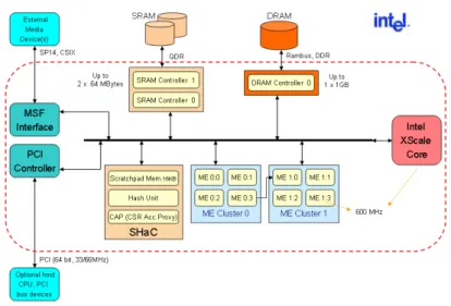
Fig. 1.22shows a scheme of the IXP2400, in which functional units and connections are presented. Often we refer to IXP2400 for specific features and data we give. The network processor contains 9 programmable processors: an Intel XScale and 8 units called microengine, which are divided in 2 cluster of 4 microengines (ME 0:0 . . . ME 1:3). The general purpose processor XScale is a RISC (Reduced Instruction Set Computer) ARM V5STE compliant, while the microengines are RISCs optimized for packet processing. From the scheme in fig. 1.22 is clear the use of memories with different sizes and features (e.g., SRAM, DRAM, Scratchpad), as well as the
Figure 1.22: Scheme of the IXP2400.
availability of shared functional units with specific purposes (e.g., MSF or the unit for hash computing). In the following, all these features will be analyzed.
1.3.2
The Intel XScale
The Intel XScale processor which is installed on network processor of Intel family IXP2XXX is compliant with the ARMv5STE architecture, as defined by ARM Lim-ited. The “T” indicates the support to thumb instructions, i.e. specific instructions which allow for passing from the 32bit modality to the 16bit one, and vice versa. This capability is useful for memory utilization purposes. Instead, the “E” indicates the support to advanced instructions of Digital Signal Processing. The processor uses an advanced internal pipeline, which improves the capability of hiding memory latencies. The support to floating point operations is not available.
Regarding the programming, the XScale processor supports real time operative sys-tems for embedded syssys-tems as VxWorks or Linux. Therefore, it can take advantage of C/C++ compilers available in this environments. In addition, it can use several development tools, as IDE (Integrated Development Environment), and debuggers. In the IXP2400 NP, the XScale runs at 600 Mhz, while in the IXP2350 it runs at 1.2 Ghz.
1.3.3
Microengines
Microengines has a specific instruction set for processing packets. There are 50 dif-ferent instructions, including the operations concerning the ALU (Aritmetic Logical Unit) which work on bits, bytes and longwords and can introduce shift or rotations
1.3 Intel IXP2XXX Network Processors
in a single operation. The support to divisions or floating point operations is not available. The microengines of IXP2400 work at 600 Mhz, instead those of IXP2350 work at 900 Mhz or 1.2 Ghz. The memory which stores the code to be executed in a microengine is the instruction store and can contains up to 4K of 40bit instruc-tions. The code is loaded on microengines by XScale processor in the startup phase. Once microengines runs, the instructions are executed in a 6-stage pipeline, requiring a clock cycle with full pipeline. Clearly, whenever jumps or context swaps happen, the pipeline must be cleared out and then filled again with instructions, thus way requiring more clock cycles.
1.3.3.1 Threads
Each microengine allows for the use of 8 thread with hardware support to context switch. This way of context switch is called “zero-overhead”, because microengines hold a series of registers for each thread; thus, whenever the context switch occurs, registers copy is not required, therefore the overhead is related only to the pipeline emptying (i.e., very few clock cycles). Processors can be configured to use 8 threads, or only 4 threads. In the latter case, only the threads with even index are activated and they have a higher number of registers. All the threads execute the same instructions, which have been read from the internal memory of microengines, by starting from the first instruction. However, it is possible to differentiate the operations for each thread by using some conditional instructions:
if (ctx==1) { . . . } else if (ctx==2) { . . . }
Each thread runs and then releases the controller to allows the other ones to run. The scheduling is not preemptive: until a threads works and does not release the controller, the other threads can not execute their code. The context switch is invoked by means of proper instructions (ctx arb) and is typically used as mechanism for hiding access latency to resources. For instance, whenever an external memory must be read, the thread release the controller before it accessing to the memory. The not preemptive approach allows for reducing issues in critical sections, i.e. parts of code in which resources which are global for threads are used and modified. If two threads access to the same register at the same time, the data in the register can become insubstantial. Therefore, the not preemptive model aid in this purpose. However, the not preemptive scheduling does not solve the issue of critical sections for threads accessing contemporaneously to the same resource and belonging to different threads. Techniques of synchronization are therefore needed. To handle the threads execution for each microengine there is a thread arbiter, i.e. a scheduler which selects the thread to run by using a round-robin policy among the active threads.
1.3.3.2 Registers
• general purpose; • SRAM transfer; • DRAM transfer; • next-neighbor.
As said above, each context has a private set of registers, therefore each bank of registers is divided in the same way among threads. In addition, there are some control Status Registers (CSRs) which allows for different operations or for configuring microengines’ functioning. General Purpose Registers (GPRs) - Each microengine have 256 32-bit registers for general purpose, which are allotted in two banks of 128 registers (called bank A and bank B). Each instruction which has as operands GPRs, requires that they belong to different register banks. Registers can be accessed in local manner for the thread (i.e., each thread accesses 32 GPRs), or in absolute manner, or in global manner (i.e., registers are accessed by all the threads as global variables). In the code, name of GPRs can follow some rules [10]. Transfer Registers - SRAM transfer registers (256 per microengine) are 32-bit registers which are used for writing and reading from SRAM memory or from the other memories or functional units in the Network Processor, such as Scratchpad memory, SHaC unit, Media Switch Fabric, and PCI (Peripheral Component Interconnects) interfaces. DRAM transfer registers are suitable for writing ad reading from DRAM and can be used in replacement of SRAM registers only for reading. Transfer registers are the main mechanism to make asynchronous operations on the memories; on a transfer register a thread writes data to be then written in memory, or from a transfer register a thread reads data which has just been read from memory. Registers’ bank is divided into two parts, one of them for writing and the other one for reading. This does not allow a wrong use of transfer registers (for instance, as GPRs). More precisely, when a transfer register is used, typically a couple of registers is available, with the same name, but writing on this register means writing on the “writing” part, while reading it means accessing the “reading” part. Also these registers can be accessed in local or global manner respecting to thread. Next-Neighbor Registers - Each microengine has 128 32-bit registers called next-neighbors. They can be used in two ways: as other general purpose registers, or as “microengine communication” registers. In the first case, if the standard general purpose registers are finished, for instance, the next-neighbor registers can be used in replacement. In the second one, they make available to the microengine with the next index the data which has just been written by the current microengine. This way, the first microengine can communicate with the second one, the second one with the third one and so on. The communication can occur through a simple writing in the registers or through the set up on the registers of a data structure called ring, which is a FIFO queue and which is accessed by means two CSRs, NN PUT ans NN GET.
1.3.3.3 Signaling
Each microengine has on tap 15 numbered signals. They are useful for the execution of asynchronous operations which concern memories and functional unit. For instance, whenever a reading in SRAM is required by a thread, the end of the operation can be