European
Nanometrology 2020
Co-Nanomet
Contents
Figures... 4 Tables ... 4 Glossary of Acronyms ... 5 Authors ... 8 Executive Summary ... 91 Introduction to European Nanometrology Strategy ... 12
2 Vision 2020 ... 15
3 Technical Background... 28
4 The stakeholders ... 31
5 Infrastructure Needs... 34
6 Summary ... 35
ANNEX A - The policy-relevance of nanometrology ... 37
A.1 Policy areas where nanometrology can be employed ... 37
A.2 From policy to measurement laboratory ... 39
ANNEX B - Current and emerging regulatory issues ... 40
B.1 Overview ... 40
B.2 Defining the measurand and quality characteristic ... 43
B.3 Measurement methods in regulatory documents ... 43
B.4 Health, safety and environmental impact ... 44
B.5 Vision for the next ten years ... 44
B.6 Action plan ... 45
B.7 SWOT analysis ... 50
B.8 Summary ... 51
ANNEX C - Nanometrology and standardisation ... 53
C.1 Overview ... 53
C.1.1 Documentary measurement standards ... 53
C.1.2 Metrology in the context of standardisation ... 54
C.1.3 New standards and measurement techniques in nanotechnology... 54
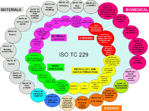
C.1.4 ISO/TC 229 Nanotechnologies ... 56
C.1.5 CEN/TC 352 Nanotechnologies ... 57
C.1.6 Other standardisation committees and related organisations ... 57
C.2 Vision for the next ten years ... 58
C.3 SWOT analysis ... 59
C.4 Action plan ... 63
2
ANNEX D - Metrology for laboratory quality assurance ... 65
D.1 Overview ... 65
D.1.1 Elements of measurement laboratory quality... 65
D.1.2 Formal quality assurance approaches ... 65
D.1.3 Specific metrological challenges for quality of measurements at the nanoscale ... 66
D.1.4 General dissemination of metrological traceability to the nanotechnology workplace ... 67
D.2 Vision for the next ten years ... 69
D.3 SWOT analysis ... 69
D.4 Action plan ... 72
ANNEX E – Technical Challenges and Opportunities ... 74
E.1 Dimensional nanometrology ... 74
E.1.1 Overview... 74
E.1.2 Vision for the next ten years ... 74
E.1.3 Action plan ... 75
E.1.4 Infrastructure needs ... 77
E.1.5 R&D strategies ... 78
E.1.6 Emerging topics and priorities ... 78
E.1.7 SWOT analysis ... 79
E.1.8 Summary ... 82
E.2 Chemical nanometrology ... 82
E.2.1 Overview... 82
E.2.2 Vision for the next ten years ... 83
E.2.3 Action plan ... 85
E.2.4 Infrastructure needs ... 88
E.2.5 R&D strategies ... 88
E.2.6 Emerging topics and priorities ... 89
E.2.7 SWOT analysis ... 90
E.3 Thin film nanometrology ... 91
E.3.1 Overview... 91
E.3.2 Vision for the next ten years ... 91
E.3.3 Action plan ... 93
E.3.4 Infrastructure needs ... 95
E.3.5 R&D strategies ... 95
E.3.6 Emerging topics and priorities ... 96
E.3.7 SWOT analysis ... 97
E.3.8 Summary ... 98
E.4 Mechanical nanometrology ... 98
E.4.1 Overview... 98
E.4.2 Vision for the next ten years ... 99
E.4.3 Action plan ... 99
E.4.4 Infrastructure needs ... 101
E.4.5 R&D strategies ... 102
E.4.6 Emerging topics and priorities ... 102
E.4.7 SWOT analysis ... 103
3
E.5 Metrology for nanostructured materials ... 104
E.5.1 Overview... 104
E.5.2 Vision for the next ten years ... 105
E.5.3 Action plan ... 108
E.5.4 Infrastructure needs ... 109
E.5.5 R&D strategies ... 110
E.5.6 Emerging topics and priorities ... 110
E.5.7 SWOT analysis ... 111
E.5.8 Summary ... 112
E.6 Electrical nanometrology ... 113
E.6.1 Overview... 113
E.6.2 Vision for the next ten years ... 116
E.7 Biological nanometrology ... 119
E.7.1 Overview... 119
E.7.2 Vision for the next ten years ... 120
E.7.3 Action plan ... 121
E.7.4 Infrastructure needs ... 122
E.7.5 R&D strategies ... 124
E.7.6 Emerging topics and priorities ... 124
E.7.7 SWOT analysis ... 125
E.7.8 Summary ... 126
E.8 Modelling and simulations for nanometrology ... 127
E.8.1 Overview... 127
E.8.2 Vision for the next ten years ... 132
E.8.3 Action plan ... 133
E.8.4 Infrastructure needs ... 134
E.8.5 R&D strategies ... 135
E.8.6 Emerging topics and priorities ... 136
E.8.7 SWOT analysis ... 137
E.8.8 Summary ... 138 ANNEX F – Infrastructure ... 140 F.1 Overview ... 140 F.1.1 Innovation infrastructures ... 141 F.1.2 Education infrastructures ... 143 F.1.3 Research infrastructures ... 145 F.1.4 Funding of infrastructures ... 146
F.1.5 Nanotechnological large-scale infrastructures in Europe ... 147
F.2 Vision for the next 10 years ... 153
F.3 Action points ... 157
F.4 SWOT analysis ... 160
F.5 Summary ... 161
ANNEX G - Education and skills ... 163
G.1 Overview ... 163
G.2 Vision for the next ten years ... 168
G.3 Action plan ... 169
G.4 SWOT analysis ... 169
4
Figures
Figure 1 Current and potential future liaisons of ISO/TC 229 ... 58
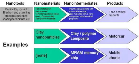
Figure 2 Nanotechnology value chain, derived from Lux Research Report on Nanotechnology ... 106
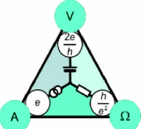
Figure 3 Electrical quantum triangle showing the relations of Ohm, ampere and voltage to fundamental constants ... 114
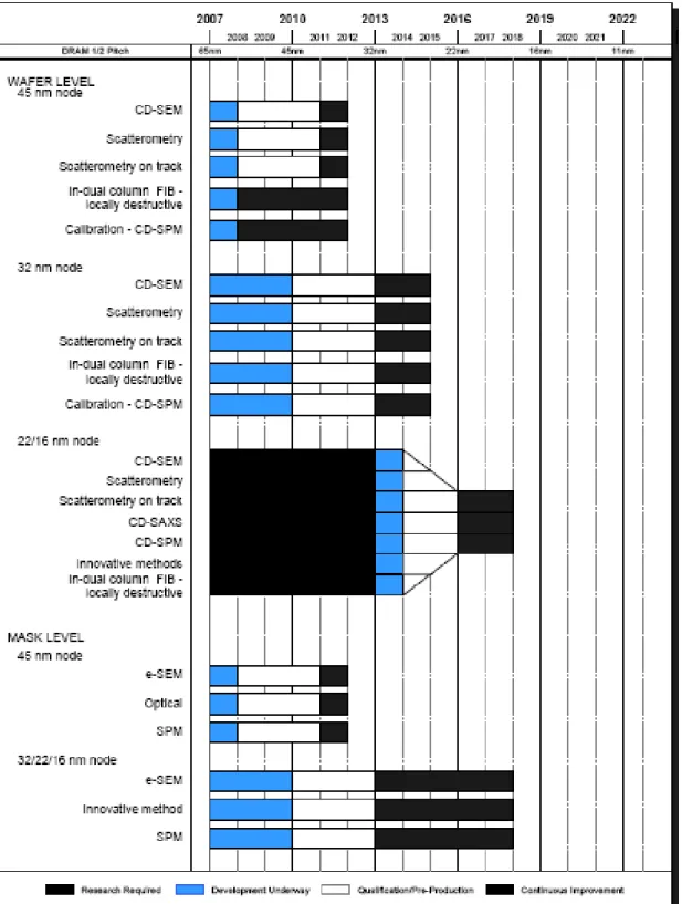
Figure 4 ITRS Roadmap 2009 Lithography Metrology Potential Solutions: CD ... 117
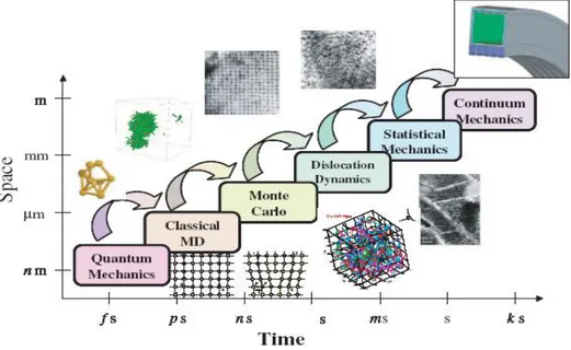
Figure 5 Models and Computer Simulations ... 127
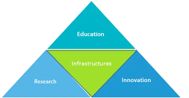
Figure 6 Infrastructures positioned within the knowledge triangle, adapted 46 ... 140
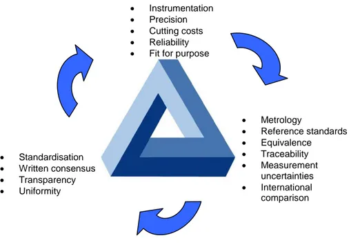
Figure 7 Triangle of standardisation, instrumentation and metrology, adapted ... 143
Figure 8 Contribution of different facility types to overall nanometrology capability 151 Figure 9 Diagram of European nanometrology infrastructure ... 156
Figure 10 Professional qualifications structure ... 167
Figure 11 Training modules structure ... 168
Figure 12 Relationships between training and professional competences ... 168
Tables
Table 1 Summary of needs for action in different technical areas ... 30Table 2 R&D schedule proposed for carbon-based nanoelectronics to impact the industry's timetable for scaling information processing technologies ... 119
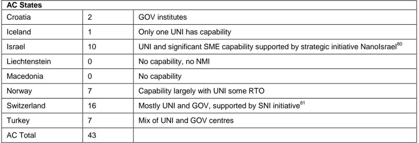
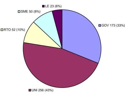
Table 3 Brief summary of identified nanometrology capabilities, continued from previous page ... 150
Table 4 NMI coverage of nanometrology capability (for example, surface texture, roundness, line spacing) from BIPM data ... 153
5
Glossary of Acronyms
AES Auger Electron Spectroscopy AFM Atomic Force Microscopy ALD Atomic layer Deposition
BEEM Ballistic Electron Emission Microscopy BIPM Bureau International des Poids et Mesures CD Critical Dimension
CEN European Committee for Standardization
CENELEC European Committee for Electrotechnical Standardization CEOC Committee of Occupational Health and Safety
CIPM International Committee for Weights and Measures CMCs Calibration Measurement Capabilities
CMM Coordinate Measuring Machine
CMOS Complementary Metal-Oxide-Semiconductor
CNT Carbon Nanotubes
CoD Centres of Dissemination CoE Centres of Excellence
CVD Chemical Vapour Deposition
CU Competence Units
DFT Density Functional Theory DUV Deep Ultraviolet
EA European Co-operation for Accreditation
EC European Commission
EC Evaluation Criteria
ECTS European Credit Transfer System
EDQM European Directorate for the Quality of Medicines EF Electric Field
EFTA European Fair Trade Association EHS Environment, Health & Safety
EMRP European Metrology Research Programme ENP Engineered Nanoparticles
EPMA Electron Probe Microanalysis ERA European Research Area
ERA-NET Networking the European Research Area ERM European Reference Materials initiative
ESFRI European Strategy Forum on Research Infrastructures ESRF European Synchrotron Radiation Facility
ETSF European Theoretical Spectroscopy Facility
ETSI European Telecommunications Standards Institute EU-OSHA European Agency for Health and Safety at Work EURAMET European Association of National Metrology Institutes EUV Extreme Ultraviolet
6 FEM Finite Element Model
FIB Focused Ion Beam
FP (6,7,8) Framework Programme (6,7,8) GENNESYS
Grand European Initiative on Nanoscience and Nanotechnology using Neutron- and Synchrotron radiation sources
GMN Gap-probed molecular nanometrology GMR Giant Magneto-Resistive Effect
HOMO-LUMO
Highest Occupied Molecular Orbit - Lowest Occupied Molecular Orbit
HPC High Performance Computing
IEC International Electrotechnical Commission ILCs Interlaboratory Comparisons
iMERA-Plus implementing metrology in the European Research Area IRMM Institute for Reference Materials and Measurements ISO International Organization for Standardisation
ITNs Initial Training Networks
ITRS International Technology Roadmap for Semiconductors
JJ Josephson Junction
JWG Joint Working Group
KCDB Key Comparison Database KPM Kelvin Probe Microscopy LCA Life cycle assessment
MBPT Many Body Perturbation Theory
MC Monte Carlo
MD Molecular Dynamics
MEMS Microelectromechanical systems MFM Magnetic Force Microscopy MLS Metrology Light Source MWCNT Multi Wall Carbon Nanotubes NEMS Nanoelectromechanical systems NGO Non Governmental Organisation
NLCG Nanotechnology Liaison Coordination Group NMI National Metrology Institute
NMR Nuclear Magnetic Resonance
OECD Organisation for Economic Co-Operation and Development OEMs Original Equipment Manufacturer
OLED Organic Light Emitting Diode PC Performance Criteria
PP Professional Performances
PRINS Pan-European Research Initiative for Nano-Structures PS Professional Skills
QA Quality Assurance
7 R&D Research & Development REACH
Registration, Evaluation, Authorisation and Restriction of Chemicals (REACH)
RM Reference Material
SAXS Small Angle X-ray Scattering
SEA Semiconductor Equipment Assessment Scheme SE Spectroscopic Ellipsometry
SEM Scanning Electron Microscopy
SEMPA Scanning Electron Microscopy with Polarization Analysis SERS Surface Enhanced Ramen Scattering
SET Single Electron Transistor SFM Scanning Force Micrsocopy
SIMS Secondary-ion Mass Spectrometry SMEs Small and Medium sized Enterprises SNAP Strategic Nanotechnology Action Plan SNOM Scanning Near-field Optical Microscopy SPIP™ Scanning Probe Image Processor SPM Scanning Probe Microscopy STM Scanning Tunnelling Microscopy SWCNT Single Walled Carbon Nanotube
SWOT Strengths, Weaknesses, Opportunities, Threats
TC Technical Committee
TDDFT Time-Dependent Density Functional Theory TEM Transmission Electron Microscopy
TM Training Module
TOF-SIMS Time-Of-Flight Secondary-Ion Mass Spectroscopy XANES X-ray Absorption Near Edge Structure
XAS X-ray Absorption Spectroscopy XPS X-ray Photoelectron Spectroscopy XRF X-ray Fluorescence
8
Authors
Theresa Burke
European Society for Precision Engineering and Nanotechnology Richard Leach, Rob Boyd, Mark Gee, Debdulal Roy, Andrew Yacoot National Physical Laboratory, United Kingdom
Hans Ulrich-Danzebrink, Thorsten Dziomba, Ludger Koenders Physikalisch-Technische Bundesanstalt, Germany
Laura E. Depero
Università degli Studi di Brescia, Consorzio Interuniversitario Nazionale per la Scienza e Technologia dei Materiali (INSTM), Italy
Kim Carneiro, Kai Dirscherl
Danish Fundamental Metrology, Denmark Valérie Morazzani
Laboratoire National de Métrologie et d’Essais, France Jukka Lausmaa, Leslie Pendrill
SP Technical Research Institute of Sweden, Sweden Allan Pidduck
QinetiQ, United Kingdom Gert Roebben
Institute for Reference Materials and Measurements (IRMM), Joint Research Centre, European Commission
Alfonso Sánchez
ASCAMM Foundation, Technology Centre, Spain Wolfgang E S Unger
Federal Institute for Materials Research and Testing, Germany Ana Proykova,
9
Executive Summary
Metrology, from the Ancient Greek metron (measure) and logos (study of), is the science of measurement. Nanometrology is a subfield of metrology, concerned with the science of measurement at the nanoscale level.
Today’s global economy depends on reliable measurements and tests, which are trusted and accepted internationally. As such, metrology is a natural and vital part of our everyday life: coffee and planks of wood are both bought by weight or size; water, electricity and heat are metered. The quantity of active substances in medicine and the effect of the surgeon’s laser must also be precise if patients’ health is not to be jeopardised.
This measurement infrastructure must be extended into the nanoscale and beyond, to bring nanotechnology based products or manufacturing processes successfully and safely into the market place. It must provide the ability to measure in three dimensions with atomic resolution over large areas. For industrial application this must also be achieved at a suitable speed/throughput.
Measurements in the nanometre range should be traceable back to internationally accepted units of measurement (e.g. of length, angle, quantity of matter, and force). This requires common, validated measurement methods, calibrated scientific instrumentation as well as qualified reference samples. In some areas, even a common vocabulary needs to be defined. A traceability chain for the required measurements in the nm range has been established in only a few special cases.
A common strategy for European nanometrology has been defined, as captured herein, such that future nanometrology development in Europe may build out from our many current strengths. In this way, European nanotechnology will be supported to reach its full and most exciting potential.
As a strategic guidance, this document contains a vision for European nanometrology 2020; future goals and research needs, building out from an
10
evaluation of the status of science and technology in 2010. It incorporates concepts for the acceleration of European nanometrology, in support of the effective commercial exploitation of emerging nanotechnologies.
The field of nanotechnology covers a breadth of disciplines, each of which has specific and varying metrological needs. To this end, a set of four core technology fields or priority themes (Engineered Nanoparticles, Nanobiotechnology, Thin Films and Structured Surfaces and Modelling & Simulation) are the focus of this review.
Each represents an area within which rapid scientific development during the last decade has seen corresponding growth in or towards commercial exploitation routes. In turn, questions of fundamental metrological understanding have emerged. The four identified thematic areas are of continuing importance for the coming decade and as key breakthrough areas with high commercial potential and societal impact.
Looking ahead to 2020, this document, sets out high level goals about each of the four priority themes. Specific objectives underpinning these goals are defined in each case plus, where relevant, underlying assumptions. This strategic analysis is captured in Vision 2020 (section 2).
Annexed to this paper is a series of more detailed reviews, supporting the Vision 2020 synopsis. These include: i) current and emerging regulatory issues (Annex B); nanometrology and standardisation (Annex C) and ii) metrology for laboratory quality assurance (Annex D). Annex E provides a detailed scientific review across eight specialist nanometrology areas (such as dimensional and chemical nanometrology). The emerging technical challenges within these areas are cross-cutting and underpinning to the four priority themes detailed above.
This document was compiled under the European Commission Framework Programme 7 project, Co-Nanomet. It has drawn together input from industry, research institutes, (national) metrology institutes, regulatory and standardisation bodies across Europe. Through the common work of the partners and all those interested parties who have contributed, it represents a significant collaborative European effort in this important field.
11
In the next decade, nanotechnology can be expected to approach maturity, as a major enabling technological discipline with widespread application. The principal drivers for its development are likely to shift from an overarching focus on the ‘joy of discovery’ towards the requirement to fulfil societal needs.
This document provides a guide to the many bodies across Europe in their activities or responsibilities in the field of nanotechnology and related measurement requirements. It will support the commercial exploitation of nanotechnology, as it transitions through this next exciting decade.
Dr Theresa Burke, Aug 2011 on behalf of the Co-Nanomet Consortium
12
1 Introduction to European Nanometrology Strategy
Introduction
Nanometrology is the science of measurement at the nanoscale (1 nm to 100 nm). It has a crucial role in the production of nanomaterials and the manufacturing of nanoscale devices with a high degree of accuracy and reliability.
As, worldwide, governments wish to see a return on their investment in nanoscience, the role of nanometrology comes to the fore. Anticipated advances in emerging nanotechnology industries will require revolutionary metrology with higher spatial resolution and accuracy than has previously been attained. Fundamentally new measurement techniques and standards must be developed.
The field of nanotechnology covers a breadth of disciplines each of which has specific and varying metrological needs. Moreover, the interdisciplinary nature of nanosciences and nanotechnology requires the development of new reference systems and concepts that can make the results of nanoscale measurements traceable and thereby comparable.
To this end, a set of four core technology fields (Engineered Nanoparticles, Nanobiotechnology, Thin Films & Structured Surfaces and Modelling & Simulation) have been assessed as part of the European Framework Programme 7 project Co-Nanomet.
Each of the four identified fields faces the challenge to develop or create new measurement techniques and standards to meet the needs of next-generation advanced manufacturing, which will rely on nanomaterials and nanotechnologies. The needs for measurement and characterisation of new sample structures and their behaviour far exceed the capabilities of current measurement science.
Framing the European Nanometrology Strategy
As strategic guidance, this document contains a vision for European nanometrology 2020; future goals and research needs, building out from an evaluation of the status
13
of science and technology in 2010. It incorporates concepts for an accelerated development of European nanometrology, in support of the effective commercial exploitation of emerging nanotechnologies.
Process for developing the Strategy
Over a two year period, the Co-Nanomet programme has carried out a comprehensive review of the current status, future challenges and opportunities.
A number of forums have been used to gather and consolidate input from key experts and interested parties including: a foresight review, the formation of five European nanometrology Action Groups including key stakeholders; targeted workshops and consultations1 throughout 2009 and 2010; publication of a series of discussion papers and the launch of a nanometrology capabilities directory mapping key capacities Europe wide. Input has been drawn from industry, academia, (national) metrology institutes, standards and regulatory bodies both European and world-wide.
This work builds on previous activities, including that carried out in the European Commission specific support action, Nanostrand, which ran from August 2006 until January 2008. An output of Nanostrand was a set of roadmaps in the areas of: (i) dimensional nanometrology; (ii) nanomechanical metrology; (iii) nanochemical metrology; (iv) nanostructured materials; and (v) nanobiometrology. The roadmaps have been drawn upon in this review.
Background to this Strategy
Nanoscience and nanotechnology involve studying and working with matter at and around the nanoscale (1 nm to 100 nm). Astonishing progress has been made in the last decade in the field. A fundamental understanding of physical, chemical and biological processes at the nanoscale has accelerated at a pace, on the basis of new measurement capabilities. For example, femtosecond observation of nanoscale interactions (displacement of atoms) has become possible in chemical processes and single-charge, single-spin, spin excitation and bond vibrations may now be
1
14
probed at the atomic scale. Meanwhile meaningful commercial exploitation has emerged: semiconductors with lateral features under 100 nm today constitute over 30 % of that market worldwide; in 2005 Abraxane® was the first US Food and Drugs Administration approved drug to use albumin nanoparticles to improve the therapeutic and safety properties of an anticancer agent2. Such progress has built on discoveries during prior decades such as C60, nanotubes; and of instrument developments such as the invention of the atomic force microscope, plus developments in electron microscopy, which has enabled the imaging of surfaces and structures with sub-nanometre-level out-of-plane resolution.
Progress during the last decade has clearly established nanotechnology as a truly revolutionary technological capability, so fundamental it will impact a myriad of industrial sectors (not least chemicals, pharmaceuticals and electronics) and, no doubt, give birth to whole new areas of technology (as today’s information age has grown out of the development of the semiconductor chip).
Almost sixty countries world-wide have significantly invested in nanotechnology research programmes. In the US, the cumulative investment in its National Nanotechnology Initiative to 2010 is over $12 billion3, placing it among the largest US civilian technology investments since the Apollo Moon-landing programme. Fierce competition, therefore, exists across the globe to extract the vast economic potential of nanotechnology.
To sustain the expected considerable growth in the number of nanoproducts, major investment in technological and manufacturing/business infrastructure is needed. This includes metrology and measurement standards (documentary and material) which can be used at the nanoscale in support of conformity assessment of nanoproducts of all kinds. Quality-assured measurements in nanometrology – including metrological traceability, measurement uncertainty and standardised definitions and, if necessary, measurement methods – provides an infrastructural support throughout the innovation process – from initial idea, through design,
2
Website: nano.cancer.gov/action/news/nanotech_news_2006-01-30e.asp
3
15
manufacture, conformity assessment and marketing – through to the finished product.
2 Vision 2020
In the next decade nanotechnology can be expected to approach maturity, as a major, enabling technological discipline with widespread application. The principal drivers for its development are likely to shift from an overarching focus on the ‘joy of discovery’ towards the requirement to fulfil societal needs4
: Addressing challenges relating to water conservation, energy management and the ageing population as well as ambitions such as those specified in Europe 2020, the EU's growth strategy for the coming decade (for a smart, sustainable and inclusive economy) is expected to come to the fore.
Key markets today are in pharmaceuticals, electronics and materials. For these, and newly emerging or assimilating ones, competitive advantage will require a rigorous understanding of the principles and methods of nanotechnology. This in turn will require significantly improved measurements with higher resolution and accuracy than has previously been envisioned. New measurement techniques and standards ((both written and material) must be developed, harmonised and characterised, combining the existing expertise of metrologists in diverse fields, to support such understanding.
As nanotechnology becomes a pervasive technology, its health and safety management throughout the lifecycle (from R&D, through manufacture to product and disposal) must become a commonplace process. So too, the reference materials, documentary standards, reference data, instruments and transferable methods and models must be made available.
Direct, non-invasive, measurement of dynamic processes will be a key step forward which will open our vision and enhance our fundamental understanding of both
4
16
nanoscale systems and nanomanufacturing processes. Major challenges also lie in the preparation of test samples, with a need to preserve delicate nanoscale features.
The nanometrology community will be required to develop the empirical understanding to ensure the metrological traceability of nanoscale (and sub-nanoscale) measurement results across instruments, and thus their comparability across organisations, and across international boundaries.
Strategic priorities
The field of nanotechnology covers a breadth of disciplines, each of which has specific and varying metrological needs. To this end, a set of four core technology fields (Engineered Nanoparticles, Nanobiotechnology, Thin Films & Structured Surfaces and Modelling & Simulation) are the focus of this review.
Each represents an area within which rapid scientific development during the last decade has seen corresponding growth in or towards commercial exploitation routes. In turn, questions of fundamental metrological understanding have emerged.
The Co-Nanomet programme has assessed the current nanometrology landscape and potential within each area (see full publications list at www.euspen.eu/nanometrology) through consultation with a range of key stakeholders (defined in section 4). European Nanometrology Action Groups have been formed, serving as a focal point for communication, co-operation and collaboration amongst participating parties and providing a framework for shared goals, priorities and strategies.
The four identified thematic areas have been confirmed, through the work of the Co-Nanomet programme, as being of continuing importance for the coming decade and as key breakthrough areas with high commercial potential and societal impact. Given a minimum incubation period of emerging capabilities of five years, and the envisioned transformation of nanotechnology in the next ten years, emphasis should
17
With the rapid speed of development in the field, an adaptive strategy is required to respond to advances in research, new discoveries and product development. Looking ahead to 2020, this document, therefore, sets out high level goals about each of the four areas. Specific objectives underpinning these goals are defined in each case plus, where relevant, underlying assumptions.
Priority Theme 1: Engineered nanoparticles (ENPs)
Nanoparticle production is in rapid growth for many different applications. Increases, in the last decade in the number of different kinds of ENPs and the broader range and understanding of their functional properties promises much for future applications. The commercial availability of off-the-shelf nanoparticles, in sizes ranging from one to one hundred nanometres, has enabled rapid advances in the fundamental science and application of particles in products ranging from medical therapeutics to hybrid electronics.
Goal for 2020: As nanoparticle enabled products expand further into the market
place, nanoparticle EHS (Environment, Health & Safety) hazard assessment is routinely integrated into mainstream research and production activities, to support safer and more equitable progress of existing and future nanotechnology generations.
Specific Objectives:
i) Development of scientifically sound classification methods to distinguish nanoparticles in terms of their basic physico-chemical characteristics and properties.
ii) Enhanced understanding of the suitability and limitations (detection limits, calibration procedures, etc.) of measurement techniques and instrumentation (in particular for the range below 10 nm) both within the scientific and industrial community. It is particularly important to be able to select the relevant measurand and methodology for a particular industrial application, and to have a full understanding of the intercomparability of different techniques.
18
relevant measurands including i) concentration measurement, ii) shape description and iii) surface charge measurement.
iv) Deterministic relationships between concentration metrics (number, surface, mass, etc.) and EHS related effect (dose, toxicity) of nanoparticles should be established.
v) Instrument calibration and method validation should be routinely established for measurements in the range below 100 nm (including accuracy, uncertainty, resolution of size distributions). Where possible, easy, robust, broadly applicable methods should be made available to measure nanoparticles in complex matrices, high concentration and/or harsh environments (pH, temperature, pressure, etc.).
vi) Improved resolution, low-noise metrology scanning probe microscopy for very small scales is required in support of nanoparticle technology development (as well as nanobiotechnology, thin films and structured surfaces). The attainment of sub-atomic resolution not only vertically (out-of-plane), but also laterally is a key objective here.
vii) Improved resolution methods for chemical analysis of nanoparticles.
Assumptions:
Development of suitable reference measurement systems (including standard methods and reference materials) iis required in support of the above objectives.
Priority Theme 2: Nanobiotechnology
This area addresses the development of nanometrology related to biomedicine, bioscience and biotechnology. This is of particular importance for the pharmaceutical industry, health care applications such as imaging technology, clinical diagnostics, and medical devices (for example, implants), as well as for food safety.
In the area of bioanalytics, medical diagnostics and biosensing there is currently an intense development of new measurement methods based on nanotechnology. Important goals of this development are increased sensitivity, selectivity, speed, cost
19
effectiveness and ease of use. Measurement challenges in this rapidly developing area include the in-situ measurement of dimensions of biological structures, localisation and measurement of relevant levels of biologically important substances (such as drugs, biomarkers and toxins), and the biological variability of systems. Characterising soft and wet materials at the nanoscale remains a challenging task to this community.
Goal for 2020: Achieve a further step change in measurement science to improve
our fundamental understanding of complex structures and phenomena within biological systems at the nanoscale and their interface with hard matter or abiotic factors. The engineering capability achieved should enable improved quality of life within the ageing population and the development of new technologies, drugs and therapies for diagnosing, understanding and treating wide spread diseases (such as diabetes, cancers, etc.).
Objectives:
i) Nanometre resolution achieved for the in-situ measurement of the three dimensional structure of a single protein with chemical specificity.
ii) Detection of low concentrations of biomolecules or disease markers below
gm-3 in biological samples.iii) Measurement of drug molecule binding to single receptors.
iv) Imaging of living systems with high spatial and temporal resolution, as well as three dimensional information from buried structures.
v) Increase of metrological awareness and understanding within the bio- and medical communities. Collaboration must be enhanced between these players and the metrology community to address this. Education activities must be further established to disseminate metrology knowledge into this new sector. vi) Lack of traceability to SI-units should be addressed within the bio-nano field.
Standardisation should be enabled by the development of relevant measurement methods, reference materials, and best practices.
vii) Effective implementation of reliable, economic and easy-to-use point of care devices for diagnostics and monitoring should be progressed as a key exploitation route of emerging measurement capability in the field.
20
Priority Theme 3: Thin films, structured surfaces and critical dimensions
This theme addresses the measurement and characterisation of surfaces, layers/coatings or geometrical features decisive for nanotechnology applications that have sizes (lateral and depth) of 100 nm and less.
Inorder to achieve a desired functional property, nearly all nanotechnology applications require precise control of the dimensions. Consequently measurement techniques are necessary which allow one to measure the dimensional properties as well as the specific functional properties, turning the characterisation of nanoproducts into an interdisciplinary task, with dimensional measurements often in a leading role.
Thin films are now integral to several major technology-based industries, including: semiconductor fabrication and microelectronics, magnetic data storage, optical components and coatings and photovoltaics. As thin film technology develops – more complex layers, tighter control over parameters, an increasing diversity of applications and environments – the challenges for measurements grow.
The ability to deterministically alter the topographic structure of a surface can have a profound effect on how that surface functions. Whilst much of this work is at the research stage, the number of products that include some form of surface structure control is growing rapidly.
Scanning Probe Microscopy (SPM), being an essential measurement technique for nanotechnology, is related to all four priority themes specified in this strategic paper. However a number of specific developments in regard to SPM are specified under this priority theme.
Goal for 2020: Thin film technologies (and associated nanometrology) developments
to have enabled further key advances to major industry sectors of societal import (including semiconductor, data storage, photovoltaics and microfluidics).
21
Unambiguous classification of structured surfaces and a significantly enhanced range of topographic properties made measureable through novel metrology methods. Improved understanding established between the functional behaviour of structured surfaces and its features and the related “technical” parameters describing these surfaces.
Specific Objectives:
i) A focus should be placed on accelerating the advance of techniques where Europe currently has a lead. This includes helium ion microscopy, low and medium energy ion scattering, time-of-flight secondary ion mass spectroscopy, spectroscopic ellipsometry and microinterferometry techniques.
ii) Instrumentation development to bridge the critical gap between 2½D to 3D scanning probe microscopy and today’s industrially available coordinate measuring machines should be progressed. The achievement of sub-nanometre resolution scanning ranges of several 100 millimetres with speeds of 1 cm2 s-1 would give Europe a critical industrial advantage.
iii) The important need for rapid non-contact measurement solutions should be addressed. Advances in sensitive optical methods such as ellipsometry and micro-interferometry have particular potential here.
iv) Issues of physical understanding and comparability with regard to key measurement techniques (e.g. AFM and alternative optical methods, and TEM as a benchmarking technique) should be addressed and widely disseminated. v) Improved understanding of tip-sample interactions in SPM, including tip shape
effects, to reduce measurement uncertainty and measurement artefacts.
vi) New measurement approaches and definitions should be implemented for porous and nanoparticle thin films for the determination of parameters such as surface area, pore sizes (diameter, shape, distribution, length, etc.).
vii) Focused efforts should be made to realise the potential of high-resolution tomography; 3D measurement parameters and extraction from data sets defined; speed and ease of use addressed.
viii) Techniques to probe surface layers at the nanoscale (and below) in air or liquid require further development to enable their application, for example, in
22
biological applications where function is critically dependent on the liquid environment.
ix) Systematic research effort is required on measurement and characterisation methods for structured surfaces addressing high aspect ratio, complex geometries and special sampling methods.
x) Development of metrology to enable manufacturing of micro- or nanoscale structured surfaces of lateral dimensions up to several metres.
Assumptions:
Effective implementation and development of inter-technique comparisons is key in this area. Round robins should be employed:
a) in establishing needs for standards (written or physical); and
b) in disseminating standards to industry and embedding best practice.
Development of nanometric physical measurement standards – across a range of selected materials is also required.
Priority Theme 4: Modelling and Simulation
In the field of nanometrology, computer models assist in designing new modes of measurements by giving an insight into background physical processes. Modellers may provide missing understanding of the physical properties for simulation technologies. On the other side, nanometrology contributes to effective modelling through the provision of precise input data. Modelling and simulations for nanometrology provide aid to:
a) fabricate and measure nanoscale devices for which numerical simulations can optimise the output, either by shortcutting device design or analysing the results of measurement;
b) predictively calculate the physical properties of nano-objects (clusters, polymers) for a bottom up design of nano-objects;
c) calculate the range in which a specific physical effect occurs, for example clusters of silicon atoms might become metallic in a small range. Then
23
metrology is necessary to measure and control such a small range; and
d) simulate measurement tasks obtained by a device under variation of internal (probe, electronic) or external (temperature, vibration, etc.) parameters to estimate measurement uncertainties.
Modelling and simulation for nanometrology is a novel field, which has recently attracted significant attention. Multiscale techniques have been developed that integrate molecular simulations with modelling techniques that can be used on the scale of micrometres and seconds. Such integrated simulations offer new possibilities to interpret experimental data and to predict the properties of new materials. The tools of theory have advanced as much as the experimental tools in nanoscience over the past decade. It has been a true revolution fuelled by increased computer power.
Goal for 2020: Modelling and simulation community to provide the ability to
realistically predict the behaviour of objects at the nanoscale for: 1. fabrication and integration processes;
2. three dimensional nanoscale metrology;
3. integration of multi-scale functional systems; and
4. measurement approaches for off-line and in-process production applications.
Specific Objectives:
i) Development of mixed numerical-experimental techniques for the modelling of manufacturing processes - solidification, 3D injection with or without reinforcement, fibres, anisotropy - and systems (virtual and accurate products). These include combinatorial chemistry and genetic techniques that open the door to the synthesis of new biomolecular materials and the creation of nano-interfaces and nano-interconnects between hard and soft matter.
ii) Application of new mathematic tools to bridge electronic (quantum-mechanics) through macroscopic (continuum-(quantum-mechanics) length and time scales.
24
which dominate nanoscale systems and are necessarily highly complex and heterogeneous.
iv) Establish capability to simulate, with reasonable accuracy, the optical properties of nanoscale structures and to model nanoscale opto-electronic devices.
v) Verification of complex nanostructure simulations involving “soft” biologically or organically based structures and “hard” inorganic ones as well as nano-interfaces between hard and soft matter.
vi) Development of enhanced self-assembly and directed assembly simulations.
vii) Theoretical and simulation approaches devised for quantum coherence, decoherence and spintronics.
viii) Development of self-validating and benchmarking methods.
ix) In the area of scanning force microscopy, theoretical models are necessary to correct for probe tip/sample interaction effects in the sub-nanometre range.
x) Develop methodologies for extracting quantitative 3D information from 2D images (preferably compatible with rapid imaging). This objective supports the 2020 goals for nanoparticles, nanobiotechnology, as well as thin films and structured surfaces as set out above.
In summary: there must be robust tools for quantitative understanding of structure and dynamics at the nanoscale and a strong link to real world and measurement values.
Assumptions:
As simulations become increasingly relevant for the planning and interpretation of experiments, so do closer links between the computer-simulation community and experimentalists working at the nanoscale level.
25
Pan-Priority Requirements:
A number of assumptions are made in regard to the coming decade for nanometrology development, which impact on each of the four strategic priority areas defined above. These assumptions are as follows:
A strategic pan–European plan and infrastructure for advanced instrumentation is required which supports the metrologically sound deployment of new nano-manufacturing capability (including but not limited to electron microscopes, scanning probe systems, and advanced optical systems)
Breakthrough initiatives towards measurements with high resolution in three dimensions should be supported; such metrology having the potential to prove transformational in each of the priority areas above.
It is important that future inter-laboratory comparisons (in the form of key comparisons and supplementary comparisons) and calibration measurement capabilities (CMCs) are registered in the Key Comparison Data Base (KCDB) of the Bureau International des Poids et Mesures (BIPM), accessible at kcdb.bipm.org. To make nanometrology more visible in the KCDB, Co-Nanomet has suggested to the BIPM to ‘flag’ KCDB entries with ‘nano’ when relevant.5
Nanoscience is a global phenomenon. In 1999, nanometrology initiated its first global inter-laboratory comparison on 1D gratings with eleven participants and, at this point in time, four supplementary CIPM comparisons have been approved and published in the KCDB Appendix B. It is important that European research continues on the dual agenda of working in global networks whilst maintaining a clear focus on specific European needs. On-going work in the field of nanoparticles is a good example of the benefit of such an approach (see Co-Nanomet report Nanometrology Discussion Papers 2011 published at www.euspen.eu/nanometrology for further details).
Whilst strengthening traceability within the National Metrology Institutes is required, it
5
Steele A G, Viallon J, Hatto P, Janssen J T, Knight A, Locascio L, Miles J R, Morazzani V, Prins S, Unger W (2010) Report on the BIPM Workshop on Metrology at the Nanoscale, 18-19 February, Rapport BIPM-2010/06, 22 pp
26
is equally important to transfer knowledge to the calibration and testing laboratories. The majority of these will be accredited laboratories operating under the Calibration Multilateral Agreement (MLA) of EA (European co-operation for Accreditation). The task of writing and disseminating the necessary calibration guides on nano-calibration at the secondary level is an important one. EURAMET could be considered the appropriate body to oversee this activity.
The collaboration between metrology and research, development, and innovation must continue to be strong as the novel field of nanotechnology matures. Metrology is closely linked to the concepts of quality control or conformity assessment in product manufacturing. Programmes aimed at encouraging small to medium sized enterprises to exploit the opportunities offered by for example new micro- and nanotechnologies, can usefully also cover nanometrology.
As industry and society place increasingly exacting demands on measurement in terms of complexity and accuracy, there is a need for more pre-normative R&D into the metrological aspects of measurement and product norms for nanotechnology.
The necessary tools for implementing legislation in Europe, in the form of (mandated) documentary standards, must be based on sound measurement concepts and methods. At present, legislation is seriously impeded by the lack of standardised terminology; standardisation is, however, progressing, and in ten years time one should see the usual relationship between standardisation and metrology, where standardisation ensures what one is manufacturing and discussing, and metrology ensures how one characterises or talks about nanotechnology issues.
Important standardisation effort has recently begun to give valuable results (see Co-Nanomet document “European Consultation on Metrological Traceability, Standards and Dissemination of Metrology in Industrial Nanotechnology”6
for further details). Unfortunately, documentary standards sometimes make reference to unrealistic and ambiguous measurement specifications and unclear requirements. It is suggested
6 L R Pendrill, O Flys, K Dirscherl and Gert Roebben 2010 “European Consultation on Metrological
Traceability, Standards and Dissemination of Metrology in Industrial Nanotechnology”, CO-NANOMET report, ISBN: 978-0-9566809-8-3 published at www.euspen.eu/nanometrology
27
that the metrological aspects of written standards are assessed and written standards describing new measurement procedures validated by an inter-laboratory comparison before their release.
Dissemination of European capability to potential users, is important to future exploitation and may be enabled through further development of the European Capabilities Directory developed under the Co-Nanomet programme.
Public opinion on nanotechnology is already strong, both because of the eye-catching and fascinating novel features of the nano-world and fear of the dangers to public health.7 A mature and convincing nanometrology infrastructure will help to give a scientifically sound picture of both the benefits and dangers of nanotechnology.
Instruments for implementation of priorities
Multiple mechanisms may be used to build consensus, implement priority activities and drive a common agenda at a European level. These include:
i) The European Metrology Research Programme (EMRP) may be used to drive issues of an underpinning or empirical nature requiring collaborative work between multiple (national) metrology institutes and their partners.
ii) Short term priorities, of a more applied or industrial nature, may be addressed through Framework Programme 7 (FP7, 2007 to 2013); medium term through Programme 8 (FP8, 2014 to 2020). Consideration should be taken to enable smaller scale projects (of limited partners or budgets e.g. <€5m) which may be more attractive for engaging smaller companies, who constitute a significant body of the industrial nanometrology community.
iii) Long term priorities, whilst highlighted in the technical annexes, are by their nature somewhat speculative. As these clarify, the latter part of FP8 may be used as a tool to address these.
7
Report on the European Commission's Public Online Consultation TOWARDS A STRATEGIC NANOTECHNOLOGY ACTION PLAN (SNAP) 2010-2015; website:
28
iv) Marie Curie Training Networks (ITNs8), the European Research Council grants and the EMRP Researcher Grant Programme may contribute to the transfer of knowledge through the promotion of multidisciplinary research.
v) The remit to ensure that the European Research Area is populated by a wide range of significant, world class, top quality instruments – open centres of excellence to inspire researchers in the major discipline of nanometrology – is that of the European Strategy Forum on Research Infrastructures. In them, training of young researchers and technicians may occur in a competitive environment; companies can also be incubated at the source of new technologies. To maximise impact, nanometrology infrastructures may be linked to related nanotechnology infrastructure developments. For example, the Pan-European Research Infrastructure for Nano-Structures (PRINS) will be a distributed facility of leading centres, smaller centres and research groups from all countries that forms a large pan-European infrastructure dealing with the ultimate silicon and heterogeneous integration to support the evolution from micro to nanoelectronics.
3 Technical Background
A further detailed analysis of the current state of the thematic areas addressed above and their current needs is given in Co-Nanomet publication Nanometrology Discussion Papers 2011 (www.euspen.eu/nanometrology).
In ANNEX E – Technical Challenges and Opportunities, a detailed scientific review is given across the specialist areas:
Dimensional metrology
Chemical nanometrology
Thin film nanometrology
Mechanical nanometrology
Metrology of nanostructured materials
Electrical nanometrology
Biological nanometrology
8
29
Modelling and simulations for nanometrology
The emerging technical challenges of these areas are contained within the four priority themes detailed in Section 2: Vision 2020 (Engineered Nanoparticles, Nanobiotechnology, Thin Films and Structured Surfaces, Modelling and Simulation).
In Annex E, each area is assessed against: i) a vision for the next ten years, ii) an action plan, iii) infrastructure needs iv) R&D strategies v) emerging topics and priorities, and finally vi) a SWOT analysis. These sections provide a jump off point for those wishing to address the goals for 2020 and supporting objectives set out for the four priority themes.
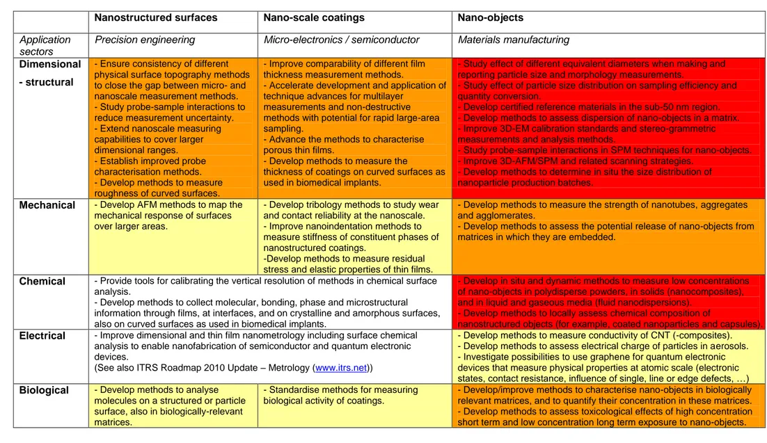
Drawing from the scientific review of ANNEX E – Technical Challenges and Opportunities, Table 1, provides a further summary of the technical needs of nanometrology and key priorities mapped to the measurement objects: nanostructured surfaces, nanoscale coatings and nano-objects. For each object, five measurement aspects (dimensional, mechanical, chemical, electrical and biological) are specified. Each field lists the most urgent topics for metrological development, which may be mapped to the priority themes above. The relative importance and urgency between fields is indicated with a colour code – on a scale from red (most urgent) to white (less urgent) as: red > orange > yellow > white.
30
Table 1: Summary of needs for action in different technical areas (Colour code: red=most urgent > orange > yellow > white =less urgent)
Nanostructured surfaces Nano-scale coatings Nano-objects Application
sectors
Precision engineering Micro-electronics / semiconductor Materials manufacturing Dimensional
- structural
- Ensure consistency of different physical surface topography methods to close the gap between micro- and nanoscale measurement methods. - Study probe-sample interactions to reduce measurement uncertainty. - Extend nanoscale measuring capabilities to cover larger dimensional ranges. - Establish improved probe characterisation methods. - Develop methods to measure roughness of curved surfaces.
- Improve comparability of different film thickness measurement methods.
- Accelerate development and application of technique advances for multilayer
measurements and non-destructive methods with potential for rapid large-area sampling.
- Advance the methods to characterise porous thin films.
- Develop methods to measure the
thickness of coatings on curved surfaces as used in biomedical implants.
- Study effect of different equivalent diameters when making and reporting particle size and morphology measurements.
- Study effect of particle size distribution on sampling efficiency and quantity conversion.
- Develop certified reference materials in the sub-50 nm region. - Develop methods to assess dispersion of nano-objects in a matrix. - Improve 3D-EM calibration standards and stereo-grammetric measurements and analysis methods.
- Study probe-sample interactions in SPM techniques for nano-objects. - Improve 3D-AFM/SPM and related scanning strategies.
- Develop methods to determine in situ the size distribution of nanoparticle production batches.
Mechanical - Develop AFM methods to map the mechanical response of surfaces over larger areas.
- Develop tribology methods to study wear and contact reliability at the nanoscale. - Improve nanoindentation methods to measure stiffness of constituent phases of nanostructured coatings.
-Develop methods to measure residual stress and elastic properties of thin films.
- Develop methods to measure the strength of nanotubes, aggregates and agglomerates.
- Develop methods to assess the potential release of nano-objects from matrices in which they are embedded.
Chemical - Provide tools for calibrating the vertical resolution of methods in chemical surface analysis.
- Develop methods to collect molecular, bonding, phase and microstructural information through films, at interfaces, and on crystalline and amorphous surfaces, also on curved surfaces as used in biomedical implants.
- Develop in situ and dynamic methods to measure low concentrations of nano-objects in polydisperse powders, in solids (nanocomposites), and in liquid and gaseous media (fluid nanodispersions).
- Develop methods to locally assess chemical composition of
nanostructured objects (for example, coated nanoparticles and capsules).
Electrical - Improve dimensional and thin film nanometrology including surface chemical analysis to enable nanofabrication of semiconductor and quantum electronic devices.
(See also ITRS Roadmap 2010 Update – Metrology (www.itrs.net))
- Develop methods to measure conductivity of CNT (-composites). - Develop methods to assess electrical charge of particles in aerosols. - Investigate possibilities to use graphene for quantum electronic devices that measure physical properties at atomic scale (electronic states, contact resistance, influence of single, line or edge defects, …)
Biological - Develop methods to analyse molecules on a structured or particle surface, also in biologically-relevant matrices.
- Standardise methods for measuring biological activity of coatings.
- Develop/improve methods to characterise nano-objects in biologically relevant matrices, and to quantify their concentration in these matrices. - Develop methods to assess toxicological effects of high concentration short term and low concentration long term exposure to nano-objects.
31
4 The stakeholders
Given the breadth of applications and implications of nanotechnology, the nanometrology stakeholder base is likewise very broad. It is convenient to separate stakeholders into two groups: public and private stakeholders. When addressing the thematic priorities set out in Section 2 - Vision 2020, the needs of each group must be taken into account.
Public stakeholders
National metrology institutes (NMIs) - NMIs have the obligation to develop and
maintain measurement standards, to provide worldwide traceable calibrations and to disseminate measurement related knowledge.
European Association of National Metrology Institutes (EURAMET) – EURAMET
coordinates, to an extent, the work of the NMIs and acts as a focal point for metrology in Europe.
Research institutions and universities - these conduct research and teach students,
and are often the starting points for work at NMIs. They frequently collaborate with NMIs and possess unique measurement instrumentation and expertise.
Regulatory bodies (National and European) – there is no, or very little, specific
regulation for nanomaterials and nanotechnology. Regulatory bodies are expected to develop new regulation, or revise existing regulation, alongside developments in nanotechnology and nanometrology9.
Calibration and testing laboratories – in the long term, nanotechnology and
fabrication must be supported by routine and accredited calibrations and test laboratories9. It is important that such laboratories are engaged in nanometrology from an early stage in order to be prepared for this novel task.
9 L R Pendrill, O Flys, K Dirscherl and Gert Roebben 2010 “European Consultation on Metrological
Traceability, Standards and Dissemination of Metrology in Industrial Nanotechnology”, CO-NANOMET report, ISBN: 978-0-9566809-8-3 published at www.euspen.eu/nanometrology
32
Standardisation bodies - work is being undertaken in national standardisation
organisations, in the European Committee for Standardization (CEN), and in the International Organization for Standardization (ISO), often in parallel. Close connections between standardisation bodies and the metrology community must be maintained, so that the new nanotechnology standards are compatible with the metrological requirements 9.
Accreditation and certification bodies – accreditation and certification bodies need to
indicate which quality assurance tools are needed to assess the performance of calibration and testing laboratories.
End-user stakeholders
Innovative industries - In order to profit from the strong European research position in
nanosciences, industry must be in close contact with new developments in metrology so that development leads to product types that can be characterised by traceable measurement results. Production industries need access to efficient, affordable calibration and testing.
Calibration and testing laboratories – in the long term, nanotechnology and
fabrication must be supported by routine and accredited calibration and testing laboratories9. It is important that such laboratories are engaged in nanometrology from an early stage in order to be prepared for this novel task.
Non-Governmental Organisations (NGOs) – many such organisations monitor
developments within the nanotechnology field, and can have a significant impact on the perception held by the general public. Metrology is essential in providing robust data in regard to developing nanotechnologies and enabling potential hazards to be made specific. Metrology ensures that risks can be estimated in concrete cases and not generalised causing unjustified public fear.
The general public – several potentially beneficial technologies have been prevented
33
based on sound measurements, will promote balance in the necessary public debate about nanotechnology.
34
5 Infrastructure Needs
In the implementation of the priority themes set out in Vision 2020 (Section 2) a number of dedicated infrastructures may be considered. Such infrastructures would work to consolidate effort at a Pan European level and enhance pathways to commercialisation of nanotechnologies. They may be applied as appropriate to the thematic area to be addressed. In some instances, a single centre may combine two or more roles of (i) measurement instrumentation hub; (ii) centre of excellence in measurement; and (iii) centre of metrology dissemination
Coordinated measurement instrumentation hubs
Because of the cost of the necessary instrumentation, and in order to ensure efficient use of it, instrument hubs may be considered in specific technology areas or, for example, for top class metrology tools of a value above €10m. Where possible these hubs should be positioned around either national metrology institutes or large scale nanotechnology infrastructures, with the provision that they be made available for wide industrial access.
Centres of measurement excellence
European centres of measurement excellence may be established in order to ensure that Europe maintains its strong research position in key areas of nanotechnology and associated metrology. The centres of excellence should be established as international, interdisciplinary centres drawing from the whole stakeholder base including industry, metrology institutes plus key research organisations. In this way nanometrology may be better positioned as an enabling part of the overall effort in contributing to major nanotechnology advances and exploitation. Such centres may provide opportunities and support for multidisciplinary research among investigators from a variety of disciplines and from different research sectors, including academia, industry and government laboratories.
The fostering of multidisciplinary research not only supports advances in knowledge, but also promotes the formation of relationships that enhance the transition of research results to a broader application base.
35 Centres of metrology dissemination
Centres of metrology dissemination may be established to ensure adequate levels of nanometrology knowledge and access to expertise for all key stakeholders across Europe. Such centres could be effectively linked with the high level priority themes defined in Vision 2020. They may foster the transfer of new technologies into products for commercial and public benefit under conditions of more rigorous understanding and controls. Hence they will also support the responsible development of nanotechnology in these fields. Linkages and input would be required from all key stakeholders including industry, NMIs, research organisations, standards and regulatory organisations and the Commission. They would provide a focal point for multiple agencies, including funding bodies, to support their planning and decision making processes for priority actions.
European industry has a further need for adequate access to calibration and test facilities and services. These centres could be established collaboratively between key partners, for example, EURAMET and the European Federation of National Associations of Measurement, Testing and Analytical Laboratories (EUROLAB) as well as relevant industry linking bodiesii.
6 Summary
Through the Co-Nanomet programme, a two year review of nanometrology status, opportunities and challenges across Europe has been carried out. The current technical status of the field and the extraordinary progress made in the last decades holds much promise for the future.
During the programme, the European nanometrology community has embraced the opportunity to work together on defining priorities and we are most grateful to all interested parties who have contributed to this review either directly or through associated work within the programmeiii.
Following a review of the field, captured in multiple publications (available at www.euspen.eu/nanometrology) and the technical annexes herein, a set of goals and
36
objectives have been established for European Nanometrology for the next decade (Vision 2020). These goals are set around the four priority themes of:
Nanoparticles
Nanobiotechnology
Thin Films and Structured Surfaces
Modelling and Simulation
The overarching aim of the priorities set out is:
a) To foster the continued growth of world class nanometrology research and development across Europe.
b) To advance the transfer of nanotechnologies into new products for public and commercial benefit under conditions of more rigorous understanding and controls.
c) To develop the supporting infrastructure, tools, embedded skills and expertise to support European nanometrology and hence nanotechnology exploitation. d) To support the responsible development of nanotechnology.
We hope this document may act as a guide to the many bodies across Europe in their activities or responsibilities in the field of nanotechnology and related measurement requirements, as it moves into its next exciting decade
37
ANNEX A - The policy-relevance of nanometrology
A
A.1 Policy areas where nanometrology can be employed
Major areas of policy in the European Union (and elsewhere), such as those identified in the recent Europe 2020 paper,10 will need the development of nanometrology, since nanotechnology can usefully be employed to meet these ‘Grand Challenges’. Flagship initiatives include:
‘Innovation Union’ to improve framework conditions and access to finance for research and innovation, in order to ensure that innovative ideas can be turned into products and services that create growth and jobs.
The Co-Nanomet project is formulating (in this document) a strategy for future research and innovation in nanometrology, in particular efficient dissemination to the workplace. Synergy with major metrology initiatives, such as the EMRP, is to be sought, for example:
‘Resource efficient Europe’ to help decouple economic growth from the use of resources, support the shift towards a low carbon economy, increase the use of renewable energy sources, modernise our transport sector and promote energy efficiency.
There are many proposals to improve energy and transport efficiency and reduce environmental emissions through the deployment of nanotechnology. Examples include ultra-light but strong nanomaterials, the new properties of which need to be carefully measured to serve as inputs to product development:
10
Europe 2020: A strategy for smart, sustainable and inclusive growth, European Commission ec.europa.eu/eu2020/index_en.htm