Alma Mater Studiorum · Università di Bologna
Scuola di Scienze
Dipartimento di Fisica e Astronomia Corso di Laurea Magistrale in Fisica
Investigation of indium tin oxide-titanium
dioxide interconnection layers for
perovskite-silicon tandem solar cells
Relatore:
Prof. Daniela Cavalcoli
Correlatore:
Dott. Jan Christoph
Goldschmidt
Dott. Armin Richter
M.Sc. Alexander Bett
Presentata da:
Jacopo Gasparetto
In questo lavoro è stato studiato ed investigato in dettaglio una nuova tipologia di stack di layer per interconnettere una cella solare a perovskite (PSC) e una cella solare etero-giunzione al silicio (SHJ) con lo scopo di realizzare in futuro una cella tandem monolitica a due terminali, ove la PSC veste il ruolo di top-cell mentre la cella SHJ quello di bottom-cell.
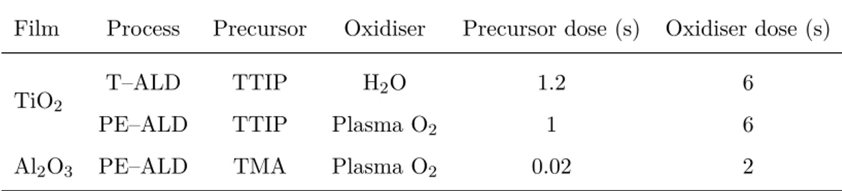
Lo stack consiste in un layer di 20 nm di indium tin oxide (ITO), depositato tramite sputtering, e un film sottile di titanium dioxide (TiO2) depositato tramite differenti
tecniche. In una cella SHJ, il layer di ITO costituisce il contatto frontale (top contact) e nel caso di una cella tandem completa svolge la funzione di recombination layer per i portatori di carica generati dalla due singole celle. Il layer di TiO2 è invece il contatto
posteriore della PSC e svolge la funzione di electron transport layer (ETL), andando a migliorare l’estrazione degli elettroni foto-generati e quindi l’efficienza della stessa.
La presente tesi si focalizza sullo studio di un sandwich ITO/TiO2/ITO, dove il film
di TiO2 è stato depositato tramite Thermal Atomic Layer Deposition (T–ALD),
Pla-sma Enhanced Atomic Layer Deposition (PE–ALD) ed Electron Beam Physical Vapour Deposition (EBPVD). Per ogni tecnica di deposizione, è stata misurata la resistenza di serie dello stack – in particolare la resistività del TiO2 bulk e la resistenza di contatto
all’interfaccia TiO2 e ITO – in funzione dello spessore del film di TiO2. Si è misurata
una resistenza di serie superiore a 15 Ω cm2 per i campioni con 20 nm di TiO
2 preparato
tramite PE–ALD e una resistenza di serie attorno ai 0.2 Ω cm2 e 0.4 Ω cm2 per campioni
con 20 nm di TiO2 preparati tramite T–ALD e EBPVD. È stato studiato l’effetto di
annealing termico sui campioni e si è osservato, in genere, un calo complessivo della resi-stenza per tutti i campioni processati con le differenti tecniche. In particolare, i campioni processati tramite PE–ALD hanno mostrato un calo significativo della resistenza, fino a valori inferiori a 0.1 Ω cm2 quando soggetti ad annealing a temperature di 225◦C per un
tempo di 15 min.
I film di TiO2 sono poi stati analizzati tramite X-ray Photoelectron Spectroscopy
(XPS) e X-ray Diffraction (XRD) per sondare la composizione chimica-stechiometrica e la struttura cristallina. Per tutti i campioni è risultato un rapporto della concentrazione atomica O:Ti di circa 2.2 con una fase amorfa, indipendentemente dalla tecnica di de-posizione del TiO2 utilizzata. Solamente dopo un annealing a 450◦C per 15 min, le fasi
cristalline del TiO2 rutile e anatase sono state osservate.
Il lavoro si è concluso con un test preliminare su celle perovskite realizzate con 20 nm di TiO2, depositato tramite le tre tecniche annunciate, su un layer di ITO di 20 nm di
spessore. La cella migliore processata tramite EBPVD ha mostrato un’efficienza pari al 13.4% e 16.8% in scansione diretta e inversa, rispettivamente, mentre la cella migliore processata tramite PE–ALD ha mostrato un’efficienza del 13.7% e 13.4% in scansione diretta e inversa. A causa di problemi durante la deposizione del TiO2 tramite T–ALD,
risultante in una deposizione parziale del film, non si è riusciti a dare una stima accurata delle efficienze delle PSC realizzate tramite questa tecnica.
I valori della resistenza di serie dello stack ITO/TiO2/ITO risultano essere compatibili
con la realizzazione di celle tandem perovskite–silicio, in particolare per quanto riguarda i campioni con layer di TiO2 depositato tramite T–ALD ed EBPVD e campioni con TiO2
depositato tramite PE–ALD trattati tramite annealing termico a 225◦C per un tempo di 15 min. I valori di efficienze ottenute per le celle solari perovskite realizzate con un layer di TiO2 depositato tramite T–ALD ed EBPVD su di un layer di ITO risultano
essere confrontabili con lo stato dell’arte. Questi risultati comprovano la fattibilità di celle tandem perovskite–silicio monolitiche dove il layer inferiore in TiO2 della PSC è
the aim to build a two-terminal monolithic solar tandem cell in the next future, where the PSC is the top-cell and the SHJ is the bottom-cell.
The stack consists in a 20 nm thick indium tin oxide (ITO) layer, deposited via sputtering, and a titanium dioxide (TiO2) thin film deposited through three different
deposition techniques. In a SHJ cell, the ITO layer is the frontal contact and in a mono-lithic tandem device plays also the role of recombination layer for the free charge carriers generated by the two cells. The TiO2 layer is, instead, the rear contact of the PSC and
covers the function of electron transport layer (ETL) which improves the extraction of the photo-generated electrons and thus, the efficiency of cell.
The focus of this thesis is the study of the sandwich ITO/TiO2/ITO, where the
TiO2 film has been deposited via Thermal Atomic Layer Deposition (T–ALD), Plasma
Enhanced Atomic Layer Deposition (PE–ALD) and Electron Beam Physical Vapour Deposition (EBPVD). For each deposition technique, the series resistance of the stack – in particular the TiO2 bulk resistivity and the contact resistance at the interface between
TiO2 and ITO – was measured as function of the TiO2 film thickness. A series resistance
above 15 Ω cm2 was measured for samples prepared with 20 nm thick PE–ALD TiO
2 and
a series resistance around 0.2 Ω cm2 and 0.4 Ω cm2 was measured for samples with 20 nm thick TiO2 prepared via T–ALD and EBPVD. The effect of thermal annealing on the
samples has been investigated and a general lowering of the resistance of all the samples differently processed was observed. In particular, the samples prepared via PE–ALD, when subjected to temperatures of 225◦C for 15 min, showed a significant drop of the resistance down to values below 0.1 Ω cm2.
The TiO2 films have been analysed via X-ray Photoelectron Spectroscopy (XPS)
and X-ray Diffraction (XRD) to identify the chemical composition (and stoichiometry) and an eventual crystalline phase. All the samples resulted with an atomic concentration ratio O:Ti of around 2.2 and they were amorphous, independently of the TiO2 deposition
technique. The crystalline phases of TiO2, rutile and anatase, were observed only after
annealing at 450◦C for 15 min.
The work ended with a preliminary test on perovskite cells fabricated with 20 nm thick TiO2 layer deposited through the three mentioned deposition techniques on a 20 nm thick
ITO layer. The best cell processed via EBPVD exhibited a power conversion efficiency (PCE) of 13.4% and 16.8% in forward and reverse scan, respectively, while the best cell processed with PE–ALD exhibited a PCE of 13.7% and 13.4% in forward and reverse scan, respectively. Because of problems occurred during the deposition of the TiO2 layer
through T–ALD, resulted in a partial deposition, an accurate estimation of the efficiency of PSC fabricated with this technique, has been not possible.
The series resistance values measured for the ITO/TiO2/ITO stack, in particular
for samples prepared with TiO2 deposited through T–ALD and EBPVD, resulted to be
prepared with PE–ALD TiO2 resulted compatible with tandem applications but after
a thermal annealing at 225◦C for 15 min. The power conversion efficiencies obtained from the perovskite solar cells fabricated with a TiO2 layer deposited via T–ALD or
EBPVD on ITO resulted to be comparable with the state of art. These results confirm the viability of perovskite–silicon solar tandem cell where the bottom TiO2 layer of the
All the experimental work and the writing of this thesis were entirely conducted at Fraun-hofer Institute for Solar Energy Systems (ISE) in Freiburg im Breisgau, Germany. The completion of this work could not have been possible without the assistance of my supervisors Jan Christoph, Alexander and Armin who helped me during the development of this thesis and taught me what doing science means.
To all the awesome people of the Novel Team for your support, help and moments spent together, to Karin, for the precious teachings in the lab, thank you. A special thanks to Patricia, for your help with this work but especially for making my stay in Freiburg unforgettable.
Thanks to my classmates and friends from the University, and to my mother, who always encouraged and supported me during my studies.
1 Introduction 1
1.1 Motivation . . . 1
1.2 Scope of this work . . . 4
1.3 Outline of this work. . . 6
2 Theory 7 2.1 Semiconductor Junction Theory . . . 7
2.1.1 Heterojunction Theory . . . 8
2.1.2 Metal – Semiconductor Junction. . . 11
2.2 Electronic transport in Perovskite-silicon Tandem Solar Cells . . . 13
2.2.1 Perovskite solar cell (PSC) . . . 14
2.2.2 Tandem device . . . 17
2.2.3 Interconnection ITO – TiO2 stack . . . 20
3 Experimental Methods 23 3.1 Film preparation . . . 23
3.1.1 Atomic Layer Deposition (ALD) . . . 23
3.1.2 Electron Beam Physical Vapour Deposition (EBPVD). . . 30
3.2 Sample preparation . . . 31
3.2.1 Dicing methods . . . 34
3.3 Perovskite solar cell preparation . . . 34
3.4 Characterisation. . . 35
3.4.1 Resistance measurements . . . 35
3.4.2 Spectroscopic Ellipsometry . . . 36
3.4.3 X-ray diffraction (XRD) . . . 37
3.4.4 X-ray Photoelectron Spectroscopy (XPS) . . . 38
3.4.5 Dark Lock-In Thermography (DLIT) . . . 39
4 Experimental Results 41 4.1 General Structure Analysis . . . 41
Contents
4.1.2 Analysis of shunt at the edges . . . 44
4.2 Resistance results . . . 46
4.2.1 Plasma Enhanced ALD. . . 46
4.2.2 Thermal ALD . . . 54
4.2.3 Electron Beam Physical Vapour Deposition. . . 59
4.2.4 General resistance comparison . . . 62
4.3 X-ray Photoelectron Spectroscopy (XPS) . . . 63
4.4 X-ray Diffraction (XRD) . . . 66
4.5 Dark Lock-in Thermography (DLIT) . . . 68
4.6 Perovskite Solar Cells Results . . . 74
1.1 (a) sketch of the light absorption mechanism in a traditional silicon solar cell: photons with energy higher than the silicon band gap are collected by the cell producing a electron-hole pair with consequent energy losses due to the thermalisation, while photons with energy lower than the band gap are not absorbed but transmitted; (b) solar spectrum absorbed by a traditional silicon solar cell. . . 2
1.2 (a) sketch of the light absorption mechanism of the two sub-cells, where the top is a perovskite solar cell and the bottom cell is silicon heterojunction solar cell; (b) solar spectrum absorbed by the two sub-cells. . . 3
1.3 Effect of series resistance on the J –V characteristic of a solar cell calcu-lated with one-diode model. . . 4
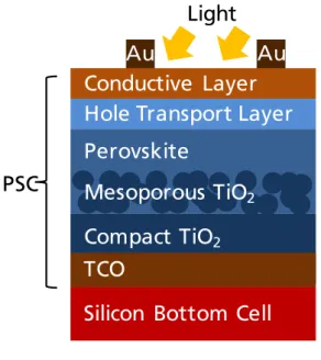
1.4 Sketch of a typical perovskite-silicon tandem solar cell, with the perovskite cell is the top cell and the silicon cell is the bottom cell. TCO stands for transparent conductive oxide. . . 5
2.1 n-p heterojunction (a) before and (b) after contact. . . . 8
2.2 Two metal – semiconductor junctions with different doping: n-type and p-type semiconductors. If the semiconductor is n-type (a), the Schottky barrier φB hinders electrons coming from the metal towards the semicon-ductor. If it is p-type (b) the barrier affects holes flowing in the same direction. In both cases a smaller barrier qVbi exists for carriers flowing
from the semiconductor to the metal. . . 11
2.3 Energy bands of some of most common perovskite absorber materials [30, 31]. In blue are shown ETLs, purple perovskite absorbers, in red HTLs. . 14
2.4 Schematic band diagram to illustrating the charge production and extrac-tion by ETL and HTL in a Perovskite Solar Cell (picture not in scale). . 15
2.5 Examples of perovskite solar cells with (a) regular planar structure, (b) regular structure with mesoporous scaffold and (c) inverted planar struc-ture. TCO refers to Transparent Conductive Oxide. . . . 16
List of Figures
2.6 Examples of perovskite solar cells with (a) planar structure with meso-porous TiO2 scaffold and (b) planar inverted structure realised at
Fraun-hofer ISE. . . 17
2.7 Scheme of a monolithic two–terminal (a) and mechanically stacked four– terminal (b) tandem devices. Shorter wavelength light is absorbed by the top perovskite cell and longer wavelengths by the silicon bottom cell as illustrated. . . 17
2.8 Electrical equivalent circuit of two solar cells in series with single diode model. . . 18
2.9 Monolithic two–terminal Perovskite–silicon tandem solar cell under pro-duction at Fraunhofer ISE. . . 20
3.1 A complete ALD cycle: during the first half of cycle (a) and (b) the first precursor, as for instance titanium tetraisopropoxide (TTIP), reacts with the substrate and the reaction stops when the whole surface is covered. In the second half (c) and (d) the oxidiser is pumped into the chamber com-pleting the reaction. When all sites are oxidised the first layer is deposited and another cycle is repeated. . . 24
3.2 Scheme of a ALD reactor featuring a RF coil for PE–ALD deposition. During a PE–ALD deposition, in the first half of the cycle the precursor is introduced in the chamber. In the second half of cycle, an inductively in-duced plasma of ionised O2 is generated through the RF coil, bombarding
the substrate and completing the deposited layer. In a T–ALD deposition, the first half of cycle is substantially the same as for PE–ALD while, in the second half, the oxidiser is introduced as water vapour. . . 26
3.3 Time evolution of a complete ALD cycle of (a) TiO2 T–ALD, (b) TiO2
PE–ALD and (c) Al2O3 PE–ALD. With different colours are depicted the
gases in the chamber. The drawing is not in scale. . . 27
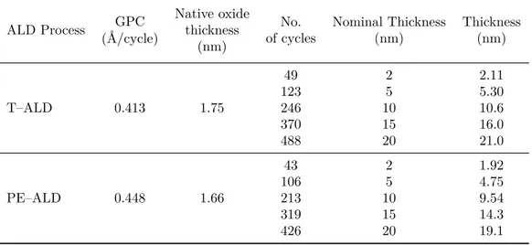
3.4 Measured thickness of TiO2 films deposited on silicon deposited by (a)
T–ALD and (b) PE–ALD in function of number of cycles used during the ALD processes. The growth per cycle (GPC) is calculated as the slope of the linear fit. . . 29
3.5 Schematic sketch of an electron beam evaporation system. . . 30
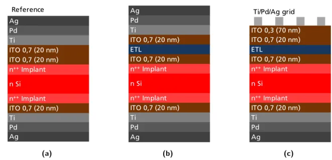
3.6 Structures analysed to investigate the resistance of the ITO/TiO2/ITO
stack: (a) reference samples without TiO2 layer; (b) samples for resistance
measurements. ETL represents TiO2 deposited with different techniques.
For some samples ETL is replaced with insulating Al2O3. (c) samples for
DLIT images. The front metal contact is replaced with a metal grid. In this case ETL indicates only TiO2. . . 31
3.7 Samples processing from the silicon substrates to the final structure. In red substrate preparation in clean room; in blue ITO/TiO2/ITO stack
depo-sition; in grey metal contact evaporation and dicing. (a) process chain for reference and resistance measurement samples shown in Figure 3.8a and (b) process chain of samples with metal grid for DLIT probe (Figure 3.8b). 32
3.8 Top view of the prepared 4-inch wafers: (a) 2× 2 cm2 metal pads evap-orated with shadow-mask for resistance measurements and (b) 2× 2 cm2
metal grids for DLIT probes. The colour blue represents the top ITO layer. The dashed lines indicate the cutting lines. . . 33
3.9 Sketch of four-point probe resistance measurements setup and electrical connections for (a) regular pad samples and (b) samples with grid metal contact for DLIT. The blue and grey colours represent the metal-coated samples. The back vacuum chuck and the connection needles are coloured in yellow. . . 35
3.10 Sketch of the interference phenomenon for ellipsometry thickness measure-ment. The polarised light is reflected at the angle θ0 at the surface, n0 is
the refractive index of the air, n1 the refractive index of the film to analyse
and n2 is the refractive index of the substrate. . . 36
4.1 Sketch of the different types of sample dicing techniques used: (a) partial engraving by laser or dicing saw from the top metal-pad contact evapo-rated with a shadow-mask; (b) complete laser cut through the wafer from the top full-metal contact; (c) partial engraving with dicing saw from the bottom, with top full-area metal contact. . . 42
4.2 Resistance measurements results after different dicing methods of differ-ently processed samples: TiO2deposited via EBPVD and PE–ALD, Al2O3
deposited via PE–ALD and reference samples without ETL. Two groups of samples with Al2O3 were fabricated with a front full-area metal
con-tact, all the others samples were fabricated with front metal-pad contacts evaporated using a shadow-mask. . . 43
4.3 DLIT investigation of three samples with different TiO2 films prepared
with a top grid-metal contact as shown in Figure 3.6c. The voltage biases were chosen to generate roughly the same total current. For similar total current flowing through the sample, brighter areas indicate a higher local current flow due to low resistive paths. . . 44
4.4 Resistance results of samples provided with top grid-metal contact used for the DLIT investigation showed in Figure 4.24 and samples provided with top pad-metal contact. These samples were used as references for samples with metal-grid. . . 45
List of Figures
4.5 Electrical scheme of the series resistance Rseries due to the TiO2 film and
the interfaces with ITO and the shunt resistance Rshunt due to the dicing
connected in parallel. . . 45
4.6 Current–Voltage characteristic of samples with 20 nm thick TiO2 film
recorded with different voltage scans: (a) 0 V− 0.7 V (forward) and 0 V − −0.7 V (reverse) scans used to calculate the total series resistance; (b) scan
from−0.5 V−0.5 V and from 0.5 V−−0.5 V; (c) scan from 0 V−2 V, from
2 V− −2 V and from −2 V − 0 V; (d) scan from −2 V − 2 V and 2 V − −2 V. 47
4.7 Resistance results of samples with different TiO2 thicknesses processed
with PE–ALD calculated fitting the J –V curves recorded in forward (0 V to +V ) and reverse (0 V to−V ) directions. The voltage bias was adjusted for each samples to limit the current below 40 mA/cm2. For more accurate
thickness values refer to Table 3.2.. . . 48
4.8 Resistance of samples prepared with PE–ALD processed TiO2 films vs the
film thickness listed in Table 3.2. In red is indicated the linear fit used to calculate the resistivity of the TiO2 and the contact resistance with ITO. 49
4.9 Thermal effect on the resistance of samples with TiO2 films prepared by
PE–ALD as function of temperature and annealing time. Two distinct groups were analysed: one set of samples with (a) the highest resistance values and one with (b) the lowest resistance values. The red is indicate the resistance of a reference samples without TiO2 film. . . 50
4.10 Detailed thermal treatment investigation for several different nominal thick-nesses of TiO2 film deposited by PE–ALD: (a) 20 nm; (b) 15 nm; (c):
10 nm; (d) 5 nm; (e) 2 nm; (f) reference samples without TiO2. Two
sam-ples were used for each thickness and as reference. . . 52
4.11 Effect of the thermal treatment on the linearity of the resistance as func-tion of the TiO2 film thickness for (a) high resistive samples and (b) low
re-sistive samples. The displayed data are the same values shown in Figure 4.9. 53
4.12 Resistance of samples with different TiO2 thicknesses, grown via T–ALD. 54
4.13 Example of J -V characteristic of 20 nm thick TiO2 film. The arrows
indi-cate the direction of the voltage scans. . . 55
4.14 Thermal treatment effect on samples with different TiO2 thicknesses films
deposited with T–ALD: (a) 20 nm; (b) 15 nm; (c) 10 nm; (d) 5 nm; (e) 2 nm; (f) reference samples without TiO2. . . 57
4.15 (a) detailed analysis of the thermal treatment on 20 nm thick TiO2 films
4.16 Resistance of samples with different TiO2 films thicknesses grown by
EBPVD in two different batches. In the first batch only samples with 20 nm thick TiO2 film were prepared. The two batches showed completely
different results without clear reason. Furthermore, three exemplary sam-ples with 20 nm thick TiO2film were annealed at 225◦C for 15 min showing
a drastic reduction of the resistance. . . 59
4.17 J –V characteristics of two samples with 20 nm thick TiO2 films deposited
with EBPVD in two distinct batches. The arrows indicate the direction of the voltage scans. . . 60
4.18 J –V hysteresis observed on samples with 20 nm thick TiO2 prepared in
the batch n.4; The numbers and the arrows represent the order and the directions of the scans: 0V → +V → −V → +V → −V → 0V . . . . 60
4.19 Thermal treatment effect on the resistance of samples with 20 nm thick TiO2 films grown with EBPVD: (a) general overview of thermal effect on
two samples; (b) reference samples without TiO2; (c) detailed investigation
of the thermal effect on samples with fixed temperature and cumulative annealing time. . . 62
4.20 Resistance values of the samples with 20 nm thick TiO2 films deposited
with electron beam physical vapour deposition (EBPVD), plasma en-hanced ALD (PE–ALD) and thermal ALD (T–ALD). For each technique, samples were realised in two separate batches. . . 63
4.21 XPS investigation of 20 nm thick TiO2 film grown on ITO with PE–
ALD: (a) and (b) overview and detailed spectra as-deposited; (c) and (d) overview and detailed spectra annealed in air; (e) and (f) overview and detailed spectra annealed in the glovebox (nitrogen). The overview scans were performed before (black) and after argon sputtering (red).The atomic concentrations were obtained from the detailed scans around the Ti2p and O1s peaks. . . 65
4.22 XPS investigation of 20 nm thick TiO2 film grown on ITO with EBPVD
and T–ALD. (a) and (b) overview and detailed spectra of TiO2 grown
with EBPVD respectively; (c) and (d) overview and detailed spectra of TiO2grown with T–ALD, respectively. The overview scans were performed
before (black) and after argon sputtering (red). The atomic concentrations were obtained from the detailed scans around the Ti2p and O1s peaks. . . 66
List of Figures
4.23 XRD spectra of: (a) 20 nm thick TiO2 films deposited on ITO through
the three different deposition techniques used. Samples in light blue and grey have been prepared in a separate batch and they have an area of
2× 2 cm2, while the other samples consist of half 4-inch wafers; (b) TiO
2
film prepared with PE–ALD after one annealing step at 225◦C for 15 min (green) and the same sample after an additional step at 450◦C for 15 min more (orange). Anatase and rutile TiO2 crystalline phases appeared after
this second step as well as peaks coming from the ITO layer underneath. In blue, the XRD spectrum of pure ITO without TiO2 is shown. All the
spectra are normalised. . . 67
4.24 DLIT images of TiO2 films grown by: (a), (b), (c) EBPVD 20 nm; (d), (e),
(f) T–ALD 20 nm; (g), (h), (i) PE–ALD 2 nm; (j), (k), (l) PE–ALD 20 nm. Three identically processed samples are shown per each TiO2 deposition
technique. The pictures have been rescaled as function of the input power of the samples. . . 71
4.25 Resistance measurements of samples with top metal-grid contact used for the DLIT investigation shown Figure 4.24. . . 72
4.26 Resistance measurements of samples with top metal-pad contact used as reference for the samples prepared with top metal-grid shown Figure 4.24 and Figure 4.25.. . . 73
4.27 Perovskite solar cells (PSCs) with 20 nm thick TiO2films acting as electron
transport layer deposited on ITO through (b) EPBVD, (c) T–ALD and (d) PE–ALD. Two ITO layers were coated with different oxygen flow: 0.3 sccm to improve the lateral conductivity and 0.7 sccm for having the same contact before and like in a tandem cell. PSCs prepared with 20 nm thick TiO2 on FTO ((a)) were used as reference cells. . . 74
4.28 Comparison of perovskite solar cells with TiO2 films deposited on ITO
trough EBPVD, T–ALD and PE-ALD. Some process problems occurred during the T–ALD deposition causing a wrong layer thickness. Cells with TiO2 deposited with EBPVD on FTO were used as reference. . . 75
4.29 (a) current–voltage characteristics of perovskite solar cells prepared with TiO2 film processed differently and (b) a zoom detail of the same
charac-teristics around the open-circuit voltage points. The slopes represent the overall series resistance of the cells. . . 76
4.30 Series resistance of the analysed PSCs obtained from two-diodes model fits to the IV curves under illumination. . . . 77
Introduction
1.1
Motivation
In the last few decades, the climate change has become more and more a global tan-gible issue, especially regarding the energy production, which is still manly based on fossil fuels. This did open a new challenge to produce energy coming from renewable and environmental friendly sources. Among these, clearly, photovoltaic energy covers a large portion thanks to its relative simplicity in modules installation and accessibility of the source, the sun. At present, most of photovoltaic modules are based on silicon cell technology due to its affordability and well consolidate knowledge, although the theo-retical efficiency limit of a crystalline silicon solar cell is calculated to be 30% [1] due to radiative recombination losses. Taking into account also Auger recombination, this limit decreases to 29.43% for un-doped silicon cells [2]. At the time of writing, the efficiency record for a fully optimised silicon solar cell is 26.7% [3, 4].
The solar energy research community is moving more and more towards new pho-tovoltaic technology concepts to overcome the efficiency limit of classic silicon cells, for example using different light absorber materials and complex structures such as tandem devices. In this kind of devices, two or more distinct solar cells work together to absorb a wider range of the solar spectrum or to reduce thermal losses of a silicon cell, with the aim to cross the efficiency limit of a single cell. In fact, a very limiting factor for traditional silicon solar cells is due to thermalisation losses that occur absorbing photons with energy higher than the silicon band gap (Figure 1.1).
Since the first appearance in late first decade of 2000s, Perovskite solar cells (PSCs) gained a lot of attention because of their extremely fast improvement in terms of efficiency [5], with efficiencies up to 22% [6], and potentially low production cost [5]. The wide and tunable band gap of PCEs is very suitable to absorb high energy photons, while the transmitted photons in the near infrared range can be absorbed by a traditional silicon cell or silicon heterojunction solar cell (SHJ). This makes them a very promising
1.1. Motivation Eɣ1 E ɣ3 Eɣ2 Ec Ev Termalisation Transmission Thermalisation (a) S p e ct ra l I rr a d ia n ce [ W m -2 nm -1] Thermalisation losses 35% (b)
Figure 1.1:(a)sketch of the light absorption mechanism in a traditional silicon solar cell: photons with energy higher than the silicon band gap are collected by the cell producing a electron-hole pair with consequent energy losses due to the thermalisation, while photons with energy lower than the band gap are not absorbed but transmitted;(b)solar spectrum absorbed by a traditional silicon solar cell.
candidate as top cell in a tandem device. In a perovskite-silicon tandem solar cell, high energetic photons are absorbed by the top perovskite solar cell, leading to more efficient photon harvesting and thus, improving the general efficiency of the solar cell, as shown in Figure 1.2.
It is possible to identify three main architectures for PSC tandem devices: separated tandem cells connected in series, monolithic two terminal cells and mechanically stacked four terminal cells [7]. Nevertheless, the monolithic two-terminal structure is probably the most investigated one because it can be fabricated as sequential depositions of all films required to realise the complete device and, most importantly, its integration in solar modules is considered much simpler.
In addition to a high quality absorber film, also the interfaces of the device play a critical role in the charge collection and then in overall performance. When a photon is absorbed by the perovskite absorber, an electron-hole pair is produced and it needs to be extracted. Similarly to a traditional p-n solar cell, where the two doped region force the free carriers to move towards the external contact, a PSC needs a Hole Transport Layer (HTL) and an Electron Transport Layer (ETL) which role is to collect free carriers out-side the absorber, creating indeed a p-i-n solar cell. In this way, the research of materials suitable to act as HTL and ETL for PSCs is of primary importance. Common HTLs are organic poly(3,4-ethylenedioxythiophene) polystyrene sulfonate (PEDOT:PSS) and 2,2’,7,7’-Tetrakis[N,N-di(4-methoxyphenyl)amino]-9,9’-spirobifluorene (spiro-MeOTAD) [8–10] or metal–oxides such as nickel oxide (NiOx) [11]. Widely used ETL materials are
tin dioxide (SnO2) [12], Zinc Oxide (ZnO) [13] and especially titanium dioxide (TiO2) [14–
Eɣ1 Eɣ3 Eɣ2 Ec Ev Transmission Top cell Bottom cell (a) (b)
Figure 1.2:(a) sketch of the light absorption mechanism of the two sub-cells, where the top is a per-ovskite solar cell and the bottom cell is silicon heterojunction solar cell;(b)solar spectrum absorbed by the two sub-cells.
electron collection efficiency and thus improves the external quantum efficiency (EQE) [6, 17]. However, having good interfaces for charge collection and transport is not the only requirement in a monolithic stacked tandem device. Also the series connection of the two sub-cells requires an interface layer between the carrier transport materials (ETL or HTL) of the PSC and the opposite equivalent (p or n) side of the silicon cell. When the p region of the first sub-cell is joined to the n region of the second sub-cells, a p–n junction is formed. At this junction, the free holes coming from the p-side of the first sub-cell recombine with the electrons coming from the n-side of the second cell, creating a space charge region at the interface. Thus, the space charge region acts as a charge emitter for both the two sub-cell, providing free electrons and holes to the first and the second sub-cell, respectively. Two routes are possible to recombine the charges at the interface of the two sub-cells: heavy doping of the two contacting layers creating a n++/p++tunnel junction or interposing a transparent contact that acts as recombination
layer between electrons and holes coming from the two sub-cells and working as an ohmic contact with very low series resistance. To achieve a highly efficient tandem solar cell, is then required to optimally tune the interconnection between the transport material (in this study the ETL) of the PSC and the top layer of the SHJ cell keeping the resistance of this interface as low as possible. In Figure 1.3 the effect of the series resistance in a solar cell is plotted. Starting with the ideal case of Rs = 0 and increasing its value it is
clear how the performance degrades rapidly. In a tandem device, the resistance of the interconnection layer(s) adds to the two intrinsic series resistance of the sub-cells. It is therefore extremely important to find the best combination of layers to maximise their charge transport capabilities and reducing, at the same time, losses due to high bulk and interface resistance.
1.2. Scope of this work
Figure 1.3: Effect of series resistance on the J –V characteristic of a solar cell calculated with one-diode
model.
1.2
Scope of this work
The scope of this work is to study the interconnection layer of monolithic perovskite-silicon tandem solar cells, with the PSC on top and a perovskite-silicon heterojunction solar cell (SHJ) as bottom cell. Typically, in SHJ the top layer is made of indium tin oxide (ITO) [18] on top of which the PSC is directly placed, creating a contact between ITO and the ETL.
Since it has been shown that PSCs exhibit higher efficiency when deposited on a mesoporous TiO2 scaffold grown on compact TiO2 [6, 15], in this work several TiO2
thin film deposition techniques on ITO are investigated and compared with the aim to optimise the interface ETL–recombination layer with low series resistance in a monolithic perovskite–silicon tandem solar cell. Also in PSCs the back contact is typically made of ITO or, alternatively, fluorine-doped tin oxide (FTO); materials widely used in the optoelectronic and photovoltaic industry thanks to their very high transparency and conductivity [19] and usually named as transparent conductive oxides (TCOs). As shown in Figure 1.4, the ITO layer is then directly in contact with the ETL (TiO2) acting as
recombination layer with the silicon bottom cell [12, 20]. Indeed, the main structure analysed in this work is a sandwich structure composed by ITO/TiO2/ITO realised on
a silicon substrate.
PSC
Au
Perovskite
Hole Transport Layer
Compact TiO
2TCO
Silicon Bottom Cell
Au
Conductive Layer
Mesoporous TiO
2Light
Figure 1.4: Sketch of a typical perovskite-silicon tandem solar cell, with the perovskite cell is the top
cell and the silicon cell is the bottom cell. TCO stands for transparent conductive oxide.
in Plasma Enhanced ALD (PE-ALD) and Thermal ALD (T-ALD) and reactive Electron Beam Physical Vapour Deposition (EBPVD). The former ideally permits a very uniform and thickness controlled deposition through a sequential deposition of single atomic layers but requires quite long deposition time and medium-high temperature (∼200◦C) and furthermore higher associated costs, while the latter allows a very fast and low cost coating at room temperature. Thermal treatments (annealing) of films at different temperatures and exposure times are then performed to study the influence on carrier transport. The results show a strong dependency of the layer electrical resistance on the annealing parameters, generally with an increase of the conductivity after the exposure. To perform the analysis, it has been necessary to design a test structure and to test different types of sample dicing methods of wafers as they can show shunts derived from the cut itself. To better understand the conduction properties of films also Dark Lock-In Tomography analysis has been performed to investigate the presence of pinholes in TiO2
films and X-ray Diffraction (XRD) in parallel with X-ray Photoelectron Spectroscopy (XPS) were performed to investigate the crystalline and chemical structure before and after thermal annealing.
The tested ITO/TiO2structures have been used to realise perovskite solar cells which
power conversion efficiencies (PCEs) have been measured and compared with the series resistance of the cells and the series resistance of the studied layers. Perovskite-silicon tandem solar cells will be investigated later on, after this work.
1.3. Outline of this work
1.3
Outline of this work
In Chapter 2, the theory of semiconductor junctions, which are the basis of solar cells, will be shown with particular attention to the heterojunction theory and their relative band structure. In Section 2.2 the description of a perovskite-silicon tandem solar cell will be presented, focusing on the charge selective layers and their role in the free car-rier collection and extraction. Afterwards, a more detailed description of the electronic properties of ITO/TiO2 stack will be given.
In Chapter 3, experimental methods employed in this thesis will be presented, starting with the detailed description of ALD and EBPVD techniques for TiO2 film depositions.
In Section 3.2 the entire sequence of the sample preparation process is presented and in Section 3.3 the of perovskite solar cells is briefly described. In Section 3.4, the used characterisation methods will be illustrated: i) the resistance measurement via a four probes setup, ii) a short description of XRD and XPS techniques to investigate the crystalline phase and chemical structure of the different TiO2 films, iii) the Dark
Lock-In Thermography (DLIT) method to investigate the possible presence of pinholes and shunts at the edges.
In Chapter 4all the results for each characterisation technique will be presented and discussed separately. At first, results from the dicing experiment, using in addition refer-ence samples without TiO2 and samples where the TiO2 layer is replaced with insulating
aluminium oxide (Al2O3), are shown in parallel with the DLIT investigation to highlight
the samples quality for current transport investigation. Then, the results of the resis-tance measurements for all the different deposition techniques before and after thermal annealing will be analysed. Finally, XRD and XPS results will be discussed to study any possible correlation between the crystalline and chemical structure with the elec-trical properties. The presented results are compared to results reported in the present literature. The chapter ends with solar cell results.
This work will be concluded with a brief outlook on all the resulted reported during the experimental work conducted.
Theory
In this chapter, the principles of semiconductor heterojunction theory are il-lustrated as collection of concepts of the most accepted and modern literature. Nevertheless, an exhaustive derivation of all aspects behind the semiconduc-tor transport theory, recombination processes and homojunction is beyond the scopes of this work and their knowledges are assumed. The following sections about heterojunction and metal – semiconductor theories are based on the
works of A. G. Milnes and D. L. Feucht [21], S. M. Sze and Kwok K. Ng
[22] and M. Grundmann [23].
2.1
Semiconductor Junction Theory
Even though tandem devices are complex structures, with several layers stacked together, and perovskite solar cells are composed of multiple layers of different materials, each interface can be still represented as a heterojunction between two different materials with unaligned Fermi levels, different work functions and band structures [24]. The same principles can be applied on the ITO/TiO2/ITO stack considered in this work. More
precisely, because of the metal-like properties of ITO, the stack can be modelled as a metal – semiconductor junction where a Schottky barrier can eventually arise.
When two semiconductor materials A and B are put in contact, according to the Anderson’s rule, free carriers coming from one of the two semiconductors, spontaneously diffuse towards the other one and vice versa, leading to a uniform Fermi level for the whole system [24,25]. From this, several ways of band alignment can arise depending on the properties of the two materials. In the simplest junction, A and B are composed by the same semiconductor with different doping, for instance p and n-silicon. This is the so-called p-n homojunction, where the two materials share the same energy gap but different position of the Fermi levels within the bands. In this junction, the alignment of the Fermi levels brings to a uniform and smooth bending of the valence band and conduction band
2.1. Semiconductor Junction Theory
(EV, EC). In a heterojunction, A and B are two different semiconductors with distinct
energy gaps. Also in this case an alignment of the Fermi levels occurs, but due to the band offset, an abrupt energy barrier can arise at the interface. A third type of junction arises when a semiconductor is kept in contact with a metal. In this case, the Fermi level (EF)
of the metal does not lie within a forbidden energy gap and the alignment of Fermi level of the only semiconductor creates eventually a Schottky barrier with rectifying properties and which sign depends on the semiconductor doping (p or n) or, alternatively an ohmic contact can take place [24].
2.1.1
Heterojunction Theory
Consider now two different semiconductors of different types, each of them characterised by its own energy gap Eg, work function ϕ and electron affinity χ which represent the
energy difference between the conduction and the valence band, the energy required to remove an electron from the Fermi level EF to the vacuum and the energy required
to remove an electron from the minimum of the conduction band EC to the vacuum,
respectively. Because of their definitions, itâĂŹs easy to see that ϕ is depending on the doping since EF position varies with it while χ is invariant.
Vacuum level EVn ECn EFn ECp EVp EFp ∆EC ∆EV φn χn χp φp n-type p-type Energy (a) EVn EVp ECn ECp Vacuum level EF ∆EV ∆EC qψbn χn qψbp qVbi φn φp χp n-type p-type Energy (b) Figure 2.1: n-p heterojunction(a)before and(b)after contact.
As shown in Figure 2.1, after the contact the difference of the two Fermi levels leads the electrons to flow from the n-type semiconductor to the p-type causing the alignment of the Fermi levels and the band bending at the interface, with abrupt steps due to the difference of conduction bands minima ∆EC and valence bands maxima ∆EV. Let us
define now qψbn and qψbp the shifts of the two vacuum levels from their original value before the contact to their new position after the contact, in respect of the interface as shown in Figure 2.1b. We can then say that the Fermi levels difference ∆EF = EFp− EFn
before the contact took place, corresponds to
EFp− EFn = q (ψbn+ ψbp) = qVbi (2.1.1.1) where the right-hand side is the difference of the two vacuum levels after the contact, Vbiis
the so-called built-in potential and q is the elementary charge of the carrier. Because after the contact EFp− EFn = 0, from the definitions of work function, the built-in potential can be also rewritten to the form
Vbi=|ϕn− ϕp| . (2.1.1.2)
The analysis of the heterojunction electronic properties is more complex compared to a simple ideal homojunction, but can be considerably simplified if we assume that band bending transition occurs only within a small region close to the interface, or alternatively that depletion region is small. This can be translated as thinking that after distances xn
and xp from the interface in the corresponding regions, the bands are completely flat,
where, for charge conservation
xn
xp
= NA
ND
(2.1.1.3) with ND and NA are the donor and acceptor atom concentrations [21]. Always using a
geometrical construction, the abrupt steps of ∆EC and ∆EV can be calculated as
∆EC = χn− χp, (2.1.1.4a)
∆EV = (Egn− Egp)− (χn− χp) . (2.1.1.4b)
It also simply follows that
∆EC + ∆EV = Egn− Egp = ∆Eg. (2.1.1.5)
What was shown so far is calculated for a n-p heterojunction, but the above equations must be valid also in the opposite case of a p-n heterojunction, taking care of signs [21]. Let us consider, for better understanding, an ideal p-n homojunction. When we treat non-degenerate semiconductors, i.e. when the Fermi level lies within the band gap
(|E − EF| ≫ kBT ), then the Fermi-Dirac distribution can be expressed by [26]
fF D(E) = 1 exp ( E−EF kBT ) + 1 ≈ exp ( −E− EF kBT ) (2.1.1.6)
that permits to calculate the free charge carrier concentrations in the two doped regions of an extrinsic semiconductor, at thermal equilibrium, by the Boltzmann relations
n0 = niexp ( EFn − Ei kBT ) (2.1.1.7a) p0 = niexp ( Ei− EFp kBT ) (2.1.1.7b)
2.1. Semiconductor Junction Theory
where ni is the intrinsic carrier concentration, Ei is the Fermi level of the intrinsic
semiconductor and kB is the Boltzmann’s constant. Even for extrinsic semiconductor the
relation p0n0 = n2i still holds at thermal equilibrium. When a bias voltage V is applied to
the junction, the carrier densities change and the Fermi levels are replaced with the quasi-Fermi levels and currents start flowing inside the device. From the continuity equations and carrier recombination dynamics it can be demonstrated that the minority-carrier diffusion currents are given [27] by
Jp =−qDp dpn dx WDn = qDppn0 Lp [ exp ( qV kBT ) − 1 ] (2.1.1.8a) Jn=−qDn dnp dx −WDp = qDnnp0 Ln [ exp ( qV kBT ) − 1 ] (2.1.1.8b)
where pn, np and pn0, np0 are the minority-carrier concentrations at non-equilibrium and
at equilibrium, Di is the diffusions coefficient, Li is the carrier diffusion length and WDi is the depletion region width of the corresponding side (i = p, n). Thus, summing up the two contribution of currents (2.1.1.8) we obtain the well known Schottky relation for the total current of the p-n homojunction
J = Jn+ Jp = J0 [ exp ( qV kBT ) − 1 ] (2.1.1.9) which is, indeed, the ideal diode equation [22].
Returning to the initial discussion about heterojunction, if one assumes that the con-dition of smooth transition (2.1.1.3) far from the interface still holds, then the relations for the diffusion currents can be applied also to the heterojunction, taking care to adjust all coefficients for the two regions. Therefore, the equations (2.1.1.8) become
Jn = qDnpn 2 ip LnpNAp [ exp ( qV kBT ) − 1 ] (2.1.1.10a) Jp = qDpnn 2 in LpnNDn [ exp ( qV kBT ) − 1 ] (2.1.1.10b) and, likewise to the total current density of the homojunction, the total current density for the heterojunction is given by [21, 27]
J = J0 [ exp ( qV kBT ) − 1 ] . (2.1.1.11)
Despite the heterojunction charge diffusion transfer characteristic (2.1.1.11) appears to be completely identical to that one of standard homojunction, its behaviour is gov-erned and tuned by the parameters of the two distinct semiconductors instead of only
one as in case of homojunction. Even though the Shockley model well predicts simply interfaces at low current densities, it is limited by several factors neglected in a first approximation, such as the presence of a parasitic series resistance, surface defects, gen-eration and recombination of carries in the depletion region and the tunnelling effects.
2.1.2
Metal – Semiconductor Junction
Evac EF EC EV φm ϕB qVbi χs φs metal n-type Energy (a) Evac EF EC EV φm ϕB qV bi χs φs metal p-type Energy (b)
Figure 2.2: Two metal – semiconductor junctions with different doping: n-type and p-type
semiconduc-tors. If the semiconductor is n-type (a), the Schottky barrier φB hinders electrons coming
from the metal towards the semiconductor. If it is p-type(b)the barrier affects holes flowing in the same direction. In both cases a smaller barrier qVbi exists for carriers flowing from
the semiconductor to the metal.
The same phenomena of Fermi levels alignment and band bending are also observed when a semiconductor is brought in contact with a metal, with the main difference that in a metal there is no energy gap and the Fermi level lies within a band. After the contact, the band structure of the metal remains substantially unaltered while, at thermal equilibrium, the free charge diffusion, responsible for the Fermi level of the semiconductor alignment with the metal one, causes the bending of the semiconductor energy bands depending on its doping. Consider now a junction between a metal and a
n-doped semiconductor, as shown in Figure 2.2a and define again the electronic affinity
of the semiconductor as χs = Evac− EC and ϕm = Evac− EC the metal work function.
When the contact takes place, if χs < ϕm, electrons from the semiconductor diffuse
into the metal, causing a shift of both EC and EV making them more negative at the
interface. As consequence, we immediately notice the presence of a barrier at interface that obstacles the electron flow from the metal to the semiconductor. The barrier takes the well-known name of Schottky barrier whose height is calculated by
φB = ϕm− χn. (2.1.2.1)
Similarly, as what we have seen previously for the heterojunction, a built-in potential Vbi is present due to the vacuum levels offset after the contact, but this time it also plays
2.1. Semiconductor Junction Theory
the role of barrier for the electrons flowing from the semiconductor to the metal and, denoting ϕs the semiconductor work function, is given by [21, 23]
qVbi= ϕm− ϕs. (2.1.2.2)
In the opposite case, when χs> ϕm, there is no barrier for electrons flowing from the
semiconductor to the metal and the junction becomes a simply ohmic contact. When, instead, a Schottky barrier is present (χs < ϕm), the metal – semiconductor junction
becomes rectifying and behaves similarly to a simply p-n junction: applying a potential difference to the junction, whenever the potential over the n-semiconductor is lower than the one on the metal (forward polarisation) the barrier φB is lowered and an electron
current is allowed. At the opposite, when the metal undergoes a lower voltage than the semiconductor (reverse polarisation) the barrier height increases creating a current interdiction, until the condition of breakdown is reached.
Under a working condition where φB ≫ kBT , that allows to neglect thermal
fluctu-ations, it is a fair assumption to say that the Schottky barrier plays a lead role in the junction overall resistivity. Because in a metal – semiconductor junction two barriers are present, the total current flowing in the device is mainly due to the privileged motion of majority charge carriers from the semiconductor to the metal since affected by a smaller barrier (qVbi< φB).
As for the heterojunction, the current density is proportional to the density of state in the conduction band and the charge transfer characteristic is calculable trough the Fermi – Dirac statistics. The complete derivation can be found in Ref. [23] and we only show that the total current density of the metal – semiconductor junction is given by
J = JS [ exp ( qV kBT ) − 1 ] (2.1.2.3) where JS is the saturation current
JS = A∗T2exp ( −qφB kBT ) (2.1.2.4) and A∗ is the Richardon’s constant for thermo-ionic electron emission
A∗ ≡ 4πem
∗ nkB2
h ≈ 120 A/(cm
2K2) (2.1.2.5)
where e is the electron charge, m∗n is the effective electron mass and h is the Plank constant. Inverting (2.1.2.4) we find that the Schottky barrier hight is
φB = kBT q ln ( A∗T2 JS ) . (2.1.2.6)
The two equations (2.1.1.9) and (2.1.2.6) represent, however, the ideal case. A more realistic illustration for the current density is given considering a series resistance RS
due to the contact and it leads to the expression [26]
J = JS [ exp ( q(V − IRS) nkBT ) − 1 ] (2.1.2.7) where we introduced the ideality factor n that takes into account any not ideal aspects, such as charge recombination or losses. Thus, the series resistance can be calculated as
RS = ∂V ∂J T (2.1.2.8) that is it negligible at low voltage allowing us to calculate n, which takes in account the charge carrier recombination and or defects, as
n = q
kBT
∂V
∂(ln J ), (2.1.2.9)
where n > 1 and n = 1 corresponds of course to the ideal case.
In the above description, we neglected every tunnelling effects trough the barrier that can effectively permit a majority carrier current also under reverse bias. This is particularly true for highly doped semiconductors, where the Schottky barrier becomes sufficiently thin to permit a tunnel current. Moreover, this simplified model only takes into account values of work functions and electronic affinities of materials before the contact, assuming that they remain unaltered after the contact, but it has been shown that these values change considerably after the contact due to defects at interface and chemical reaction between the two components.
2.2
Electronic transport in Perovskite-silicon
Tan-dem Solar Cells
To better understand the electronic transport within a perovskite-silicon tandem solar cell, it is necessary to describe a perovskite solar cell, to define the role of its components and to clarify why it requires a well defined stack of selective contact layers for charge harvesting and collection. As these layers are necessary to have a significant power con-version efficiency (PCE) in a single PSC, in a tandem device the stack of all required layers must be designed to avoid any current losses at the interface between the PSC and silicon bottom cell as much as possible. It is also quite obvious that, in addition to having perfect electronic properties, these materials must also be optically transparent in the wavelength ranges used by the two cells, to guarantee a good energy conversion of incoming photons.
2.2. Electronic transport in Perovskite-silicon Tandem Solar Cells
2.2.1
Perovskite solar cell (PSC)
With perovskite, a wide group of chemical compounds is meant, represented by the raw formula ABX3 where A and B are two cations and X is an anion, with A larger than
B [5, 28, 29]. In photovoltaic applications, the perovskite absorbers are mainly made of organic–inorganic halide perovskites, where A is usually methlyammonium (CH3NH+3
or simply MA) or ethylammonium (CH3CH2NH3+) and B is commonly Pb, while the
anion X is a halogen like I, Br, or Cl. At present time, the most studied perovskite structures are methylammonium lead triiodide (CH3NH3PbI3 or MAPbI3) and mixed
(or hybrid) halide compounds such as MAPbI3−xClx and MAPbI3−xBrx[5, 16]. Other
perovskite materials currently under investigation are CH(NH2)2PbI3, MASnI3, CsSnI3
and more [24]. For all of them several deposition techniques are possible, such as spin coating or evaporation.
Figure 2.3: Energy bands of some of most common perovskite absorber materials [30, 31]. In blue are shown ETLs, purple perovskite absorbers, in red HTLs.
The great attraction of these materials is due to several key features that make them perfect candidates for photovoltaics applications and in particular for tandem devices: a wide and tunable energy gap within the range of about 1.55 eV and 2.28 eV, high absorption coefficients and long carrier diffusion lengths [29, 32, 33]. However, a fully working PSC is not complete until the perovskite absorber is embedded in between an Electron Transport Layer (ETL), and a Hole Transport Layer (HTL) which perform the
function of collecting and extracting the charge carrier generated within the perovskite [6].
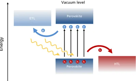
Figure 2.4: Schematic band diagram to illustrating the charge production and extraction by ETL and
HTL in a Perovskite Solar Cell (picture not in scale).
When an incoming photon is absorbed by the perovskite material, a hole – electron pair (exciton) is generated. While in organic absorber materials the exciton is strongly bound and, after its diffusion to the interface, needs to be dissociated in free carriers, in perovskite materials, instead, the exciton binding energy is much lower making PSCs “silicon-like” solar cells where the photon absorption and the consequent free carrier generation are almost instantaneous [34].
ETLs and HTLs are specifically designed to have a particular energy band struc-ture to favour the extraction of one type of charge carriers. In Figure 2.3 some of the most used and investigated ETL and HTL with their respective band structures are re-ported. In particular, the former must have the minimum of the conduction band EC
close in energy with the minimum of the conduction band of the perovskite absorber while the latter must have the maximum of the valence band EV close to perovskites
valence band in the way to collect a hole and electron, respectively (Figure 2.4). Hav-ing a good band alignment between the transport layers and the perovskite absorber means also to reduce energy barriers at the interface, in particular the built-it po-tential, that can occur. In other words, the small mismatch between the conduction band of ETL and the valence band of HTL with the correspondent perovskite band edges favours the formation of an ohmic contact. In addition to an energy barrier re-duction, and thus, a current transport losses, good band aligment increases the final open–circuit voltage (VOC) of the solar cell [35]. The most used ETLs are TiO2, ZnO,
2.2. Electronic transport in Perovskite-silicon Tandem Solar Cells
spiro-MeOTAD, PEDOT:PSS and poly(triaryl amine) (PTAA).
Metal contact (Au)
Perovskite HTL ETL TCO Glass substrate Au (a)
Metal contact (Au) Perovskite HTL ETL TCO Glass substrate Au Mesoporous scaffold (b)
Metal contact (Au)
Perovskite ETL HTL TCO Glass substrate Au (c)
Figure 2.5: Examples of perovskite solar cells with (a) regular planar structure, (b) regular structure with mesoporous scaffold and (c) inverted planar structure. TCO refers to Transparent
Conductive Oxide.
PSCs can have many different structures depending on different layer arrangements. The first common distinction is between the so-known regular and inverted structure. Since there is no actual preferred illumination direction (both structure can be ideally illuminated from both sides), it is commonly accepted to call the structures regular structure or n-i-p, when the ETL is the first layer deposited on the glass substrate (Figure 2.5a). Contrariwise, the inverted structure, or p-i-n, is commonly referred to cells where the HTL is the first layer deposited on the substrate (Figure 2.5c). From here onwards we will use this convention.
Since the first attempts with PSCs it has been shown that perovskite grown on electron conductive mesoporous scaffolds exhibit higher efficiencies thanks to a higher electron injection, better perovskite growth and stability [6, 15, 17, 36, 37]. As shown in Figure 2.5b, the perovskite absorber is deposited directly on the mesoporous scaffold generally made of TiO2 or Al2O3, creating nanoparticles inside the scaffold its self. In
most cases the mesoporous layers were produced with a sintering step at high temper-atures. This limits the choice of the substrate as well as can damage the bottom cell during the processing of a tandem device. Currently, many research groups are studying different routes to achieve the same efficiency and stability without using a high tem-perature sintered mesoscopic scaffold, to enable the PSC integration on substrates and devices that require low temperature processing. Examples are the planar structure with compact ETL (Figure 2.5a) or TiO2 nanocompound solutions [38–40]. Furthermore, a
new route for low temperature mesoporous TiO2 by UV curing has been recently
devel-oped at Fraunhofer ISE [37].Figure 2.6 shows two examples of PSCs studied at Fraun-hofer ISE with mesoporous TiO2 scaffold (Figure2.6a) and one with inverted structure
Au CH3NH3PbI3 Spiro-OMeTAD Compact TiO2 FTO / ITO Glass substrate Au Mesoporous TiO2 (a) Perovskite PCBM + AZO PEDOT:PSS ITO Glass substrate Ag Ag (b)
Figure 2.6: Examples of perovskite solar cells with(a)planar structure with mesoporous TiO2 scaffold
and(b)planar inverted structure realised at Fraunhofer ISE.
2.2.2
Tandem device
I = Min(I1,I2) Top Perovskite Solar Cell Bottom Silicon Solar Cell (a) I = Min(I1,I2) Top Perovskite Solar Cell Bottom Silicon Solar Cell (b)Figure 2.7: Scheme of a monolithic two–terminal(a) and mechanically stacked four–terminal(b) tan-dem devices. Shorter wavelength light is absorbed by the top perovskite cell and longer wavelengths by the silicon bottom cell as illustrated.
Perovskite-silicon tandem solar cells are mainly built with the two configurations shown in Figure 2.7: the monolithic two-terminal tandem structure or the mechanically stacked four-terminal tandem. Because of their energy gaps, in both cases the perovskite cell is placed on top to absorb photons with shorter wavelengths, while the silicon bottom cells is designed to absorb the photons with longer near infrared wavelengths [20, 41]. The four-terminal tandem is easier to realise since the two cells are fabricated separately. On the other hand, the two-terminal monolithic tandem has the advantage of requiring a lower number of fabrication steps as well as a lower number of electrodes, leading to potentially reduced overall manufacturing costs [41]. The advance of the two–terminal
2.2. Electronic transport in Perovskite-silicon Tandem Solar Cells
tandem solar cells is mainly due to the easiness of the integration in modules, since less electrical connections are required and simpler electronic control unit are required, compared to a four–terminal device, where the two subcells must be handled seperately (Figure 2.7).
However, monolithic tandems are not free of inconvenience since they require a chain of compatible processes for the two sub-cells. As already mentioned, perovskite cells with mesoporous TiO2 scaffold exhibit higher performance but they are obtained with high
temperature sintering. While high temperatures are compatible with c-Si sub-cells, they are problematic for high efficient a-Si:H/c-Si heterojunction cells (SHJ), which have been shown to suffer thermal instability and degradation for temperature above 200◦C [20]. Another crucial aspect, that holds generally for all types of tandem cells, is that the perovskite top cell must maximise the absorption within its working wavelength range and simultaneously be transparent in the near infrared to permit the silicon bottom cell to absorb the lower energy photons (Figure 2.7).
This requirement is also equally mandatory for the interconnection layer which role is to electrically contact the two cells. For this task, transparent conductive oxides (TCO) are utilised as recombination layer of minority carriers and ohmic contact, such as indium tin oxide (ITO), indium zinc oxide (IZO) or aluminium doped zinc oxide (ZnO:Al) [42,
43]. The importance to have a good ohmic contact is to reduce the energy barrier for the majority carriers that could lead to recombination at the interfaces and then to a total current degradation [44, 45]. Rp1 Rs1 Rp2 Rs2 Voc Jsc1 Jsc2
Figure 2.8: Electrical equivalent circuit of two solar cells in series with single diode model.
From an electrical point of view, we can describe a two–terminal tandem device as two distinct solar cells connected in series (as displayed in Figure 2.8). It follows that the total current flowing in the device must be the same for both cells. Because of the two current generators Jsc1 and Jsc2, representing the sub-cells short circuit currents, the
total current is dominated by the smaller of them. Moreover, for a given current, the total output voltage V must be the sum of the two output V1 and V2 produced by the
two individual subcells at the same current. Another requirement resulting from series connection is that the bias of the two sub-cells must have the same sign. In other words,
this means that, if p-side of the top cell is under illumination, the p-side of the bottom cell must be connected to the n-side of the top cell. To connect the two sub-cells, two routes are possible. One is to interpose a transparent conductive oxide (TCO) between the p and n sides of the two cells, as illustrated in Figure 2.9. Such kind of contact leads to a recombination of electrons coming from the n-side of the top cell with the holes coming from the p-side and the TCO acts as carriers emitter for the two sub-cells. In this way, the majority carriers flow with the same direction along the whole tandem cell and they can be collected out by the two metal contacts. A second option is to replace the TCO with two oppositely highly doped semiconductors (n++/p++) creating a tunnel junction at the interface. But because of the high dope, then the tunnel junction becomes very thin and the free carrier absorption can be enough small to not significantly compromise the overall performance [46], allowing also in this case the recombination between holes and electrons near to the interface.
2.2. Electronic transport in Perovskite-silicon Tandem Solar Cells
Hole contact (Spiro-OMeTAD)
Interconnection layer (ITO)
Silicon absorber
Perovskite absorber (CH3NH3PbI3) Transparent conductive top layer (ITO)
Electron contact (TiO2) Hole contact (a-Si:H(p))
Metal front grid
Mesoporous scaffold (TiO2)
Metal rear contact Electron contact (a-Si:H(n))
Figure 2.9: Monolithic two–terminal Perovskite–silicon tandem solar cell under production at
Fraun-hofer ISE.
2.2.3
Interconnection ITO – TiO
2stack
As already mentioned, the top layer of silicon heterojunction solar cells (SHJ) is generally made of ITO [18], while PSCs studied at Fraunhofer ISE present a low temperature processed mesoporous TiO2 scaffold coated on a compact TiO2 layer. It is then clear
that is necessary to investigate the properties of the at the interface between the ITO and compact TiO2 layers, where ITO, in addition to be the front contact of the SHJ cell,
plays the role of recombination layer for this kind of device.
TiO2 exists in several different phases, amorphous and crystalline phase such as
Anatase or Rutile or, more likely, in mixtures of them and its chemical composition can also vary in a more realistic form of TiOx. For these reasons, it is not a trivial task
to define electronic properties of this material that are also affected by the deposition techniques, which can produce defects in the bulk as well as at the surface. Nevertheless, TiO2 is typically a n-type semiconductor with an estimated energy gap of
approxima-tively 3.0 eV− 3.3 eV [31,47] and electronic affinity about 4.1 eV− 4.4 eV [48,49]. ITO, instead, is a heavily doped n-type wide band gap semiconductor (Eg =∼3.5 eV−4.3 eV)
with the Fermi level EF located very closely to the conduction band maximum EC [19].
Thanks to these properties ITO is so well conductive that it can be considered metal–like but still transparent in the low visible and the near infrared range. Depending on the surface treatment and deposition technique, ITO work function ϕm can vary considerably
[50]. Nevertheless, the most accepted value of ITO work function is about 4.7 eV [51–53] Considering ITO as a pure metal, the ITO – TiO2interface can be modelled as a metal
– n-type semiconductor junction where a Schottky barrier is present, since ϕm > χsand a
rectifier behaviour is expected. In reality, it has been shown that, even if the barrier height cannot be modified as it depends on the fixed values ϕm and χs (equation (2.1.2.1)), its
TiO2 can be quite different depending on the deposition technique and can be changed
with post-deposition treatment like annealing or UV irradiation [48, 54] and thus, the probability of tunnelling through the barrier is significantly enhanced. If this would be the case, then a good ohmic contact with sufficiently low resistance could be achieved maintaining the electron transport properties of TiO2.
Experimental Methods
In this Chapter, a detailed description of the used experimental methods is presented, with particular focus on the Atomic Layer Deposition and the
Elec-tron Beam Physical Vapour Deposition used for thin TiO2 film coating.
After-wards, the preparation of the samples and the characterisation methods used
to study the electrical and physical properties of the ITO/TiO2/ITO stack
are described.
3.1
Film preparation
3.1.1
Atomic Layer Deposition (ALD)
Atomic Layer Deposition is a thin film deposition technique that permits to grow a wide selection of materials from vapour gases (precursors). Although it relies on the chemical reactions of two precursors with the substrate, it differs from a traditional chemical vapour deposition (CVD), where the reactants are introduced simultaneously in the reaction chamber. During ALD, the precursors are introduced sequentially in two separate steps and they chemically adsorbed on the layer deposited in the step before. The main advantage of ALD is that the two reactions are self-limited, guarantying a very precise control of the deposition process due to a monolayer by monolayer growth, and thus of the thickness, as well as a very high homogeneity of the films surface [55–58].
Figure3.1 shows a complete ALD cycle: during the first step, the first reactant is introduced into the reaction chamber and it is adsorbed onto the substrate until the surface is completely covered forming one monolayer. Because of the self-limiting reac-tion, the gas remaining in the reactor, plus any eventual reaction product, is purged out by an inert purging gas, such as pure nitrogen or argon. Therefore, the second step of the process starts introducing the second precursor that reacts with the monolayer just deposited by the first reactant until the surface is again completely covered. Once the