1
"This is the peer reviewed version of the following article: F. Brunetti, A. Operamolla, S. Castro-Hermosa, G. Lucarelli, V. Manca, G. Farinola, and T. M. Brown, “Printed solar cells and energy storage devices on paper substrates”, Advanced Functional Materials, vol. 29, 1806798 (2019) which has been published in final form at
https://onlinelibrary.wiley.com/doi/10.1002/adfm.201806798. This article may be used for non-commercial purposes in accordance with Wiley Terms and Conditions for Use of Self-Archived Versions."
DOI: 10.1002/adfm.201806798
Article type:Review
Title: Printed solar cells and energy storage devices on paper substrates
Francesca Brunetti*, Alessandra Operamolla, Sergio Castro-Hermosa, Giulia Lucarelli, Valerio Manca, Gianluca Farinola, and Thomas M. Brown*
Prof. Francesca Brunetti, Sergio Castro-Hermosa, Giulia Lucarelli, Valerio Manca, Prof. Thomas M. Brown
CHOSE (Centre for Hybrid and Organic Solar Energy), Department of Electronic Engineering, University of Rome Tor Vergata, Via del Politecnico 1, 00133 Rome, Italy E-mail: [email protected], [email protected]
Dr. Alessandra Operamolla, Prof. Gianluca Farinola
Dipartimento di Chimica, Università degli Studi di Bari, via Orabona 4, I-70126 Bari, Italy
Keywords: flexible electronic, printed electronics paper, photovoltaics, energy storage, green electronics
Paper is a flexible material, commonly used for information storage, writing, packaging or specialized purposes. It also has strong appeal as a substrate in the field of flexible printed electronics. Many applications, including safety, merchandising, smart labels/packing, chemical/biomedical sensors, require an energy source to power operation. Here we review progress regarding development of photovoltaic and energy storage devices on cellulosic substrates where one or more of the main material layers are deposited via solution processing or printing. Paper can be used simply as the flexible substrate or, exploiting its porous fibre-like nature, as an active film by infiltration or co-preparation with electronic materials. Solar cells with efficiencies of up to 4% on opaque and 9% on transparent substrates have been demonstrated. Recent developments in paper-based supercapacitors and batteries are also
2
reviewed with maximum achieved capacity of 1350 mF cm-2 and 2000 mAh g-1 respectively. Analysing the literature, it becomes apparent that more work needs to be carried out in continuing to improve peak performance, but especially stability and the application of printing techniques, even roll-to-roll, over large areas. Paper is not only environmentally friendly and recyclable, it is thin, flexible, low-weight, biocompatible, and low-cost.
1. Introduction
Paper is a flexible material, commonly used for information storage, writing, packaging or specialized purposes like, for instance, sanitary tissues. The main world manufacturers of paper are China (26.5% of the total), the European Community (22.5%), USA (17.9%) and Japan (6.5%) with an estimated world production of ≈420 billions of kg per year.[1] The starting pulp material, like the Northern Bleached Softwood Kraft (NBSK fibres), has a cost of ~1000-1100 $/t. Paper is produced by pouring a pulp slurry on a screen, followed by dewatering, pressing, and drying with the aid of a paper machine.[2] It is composed by a web of cellulose fibres, intimately interconnected thanks to the formation of inter-fibre hydrogen bonds. Paper is not only environmentally friendly and recyclable, it is thin, flexible, low-weight, ubiquitously available, biocompatible, biodegradable, has a low thermal expansion coefficient (CTE~28-40 ppm K-1)[3] and, most importantly, is low-cost: the final product has prices between (0.3–3 $/m2).[4] Products made on paper are present from centuries in everyday life, but recently they have gained new interest due to the deep comprehension of their chemical and morphological properties.[2] This knowledge permits paper modification and its modern applications in innovative technologies. Paper represents an appealing substrate for flexible electronics: the thermal stability of cellulose, withstanding temperatures up to 250°C and decomposing at 300 °C, its recyclability can make it a preferable choice for some applications in comparison to more expensive plastics like poly(ethylene terephthalate) (PET).[5]
3
Furthermore, it exposes a high surface area for the absorption and storage of reagents. This opportunity makes paper very attractive for energy storage systems and all the related devices where high surface area is required. [6] Conversely, when considered for thin film devices application, standard uncoated paper presents some disadvantages, such as microscale surface roughness (1-10 micron), opaqueness, high porosity (10-30%) with large pores (1-5 micron), hygroscopicity, poor dimensional stability (1-5%) when moisture level in ambient changes [7]. The possibility to tailor paper characteristics allowed to mitigate some of these obstacles; for example, the surface roughness has been reduced applying coating layers, [8,9] or engineering papers based on microfibrils or nanofibrillated cellulose (NFC) which provide smoother substrates if compared to regular paper.[10]
The natural compatibility of paper with printing has allowed the application of several patterning techniques for the deposition on paper of active inks. Techniques as blade coating, slot die coating, spray coating, screen printing, inkjet printing, flexographic printing, gravure printing, dispenser printing, stencil printing have been demonstrated on paper offering also the possibility a straight path for scaling up of the production process.[11] The possibility of using paper as substrate for electronics has been proposed more than 50 years ago [12,13] however, it took more than 30 years to demonstrate the first simple electronic components and circuits, which was a smart pixel, on paper. [14] Nowadays, several devices have been demonstrated on paper such as thin film transistors, memories, organic light emitting diodes, sensors. [15,16,25,17– 24]
The use of paper in electronics has followed two main approaches; in the first case, paper is used simply as the flexible substrate where the different devices are printed; in the second case additional functionalities are given to the cellulosic paper, such as for example transparency or conductivity, allowing its use as an active material.[10] For the realization of integrated systems, paper-based devices of different sizes often require the power supply; this aspect is crucial and has received increasing attention from the scientific community. [26] Several possible
4
technologies have been demonstrated as power supplies, in particular, photovoltaic devices, supercapacitors and paper batteries, represent a viable low cost route for printable energy generation and storage system on paper.[4,6,27–30]
The integration of solar cells into portable electronic devices and consumer products, such as sensors, gadgets, and smart objects, imposes a stringent requirement in terms of weight, mechanical properties and cost of photovoltaic (PV) devices. Ideally, solar cells should be fabricated by simple and cost-effective printing processes[31], and in a light-weight and flexible form, to enable a seamless integration into consumer electronics; moreover, the life cycle assessment of the device, and therefore its disposability, should be also taken into account when designing a solar device. In this context, paper act typically as substrate, becoming a solution for the low-cost, efficient and environmentally friendly electronics of the future, being abundant, renewable, recyclable, and simple and easy to fabricate and functionalize.
On the other side, storage devices, such as supercapacitors and Lithium based batteries, ( Li-ion, Li-S and LiO2), play a fundamental role due to ease of fabrication and integration with other electronic devices as well as providing excellent performances in terms of power and energy supplied.[6,32,33] These types of devices are typically formed of several parts: the electrodes (cathode and anode), the separator, the electrolyte, the current collector and the packaging.[34] Paper here, can act as a substrate for flexible electrodes, which can be printed with several techniques, as separator or, in the case of paper-like film structures, even as s self-standing paper based electrode. In the latter case, the electrodes are obtained assembling the conductive materials in a paper-like film structure. The porous surface of paper, can be exploited to infiltrate conductive materials as high effective area electrodes, facilitating electron collection, or as a separator facilitating ion transport. [6]
Other types of electrodes, often described as “paper-like” that include free-standing, self-supporting films made with electrically conductive materials (typically carbon based) do not
5
actually contain cellulose. The advantage of this type of electrode consists in a higher flexibility with respect to paper-based electrodes, higher electrochemical performances and lower resistivity, which make them promising for high power, high density energy storage devices. In this review, this type of electrodes will not be discussed, being out of scope; for an exhaustive analysis, please consider the paper of Yao et al. [34]
Here we will present a detailed analysis on the state of the art of the use of paper and cellulose-paper like systems for the realization of photovoltaic devices, supercapacitors and batteries where at least one of the main constituent layers has been deposited or synthesized via printing or solution processing techniques. In particular, we will cover research progresses on the engineering of paper as substrate for photovoltaic and storage devices (Section 2). Subsequently, the printing techniques that have been utilized so far for the manufacturing of these devices will be discussed in Section 3. Paper photovoltaics and storage will be presented in Section 4 and Section 5 respectively, while in Section 6 we will report on durability and recyclability issues.
2. Paper as substrate for printed light harvesting and energy storage devices
The substrate represents a key part in the fabrication of devices for energy harvesting and storage. Typically, the properties of the substrate have to be tailored considering different parameters such as the type of device, its durability, the architecture chosen, the deposition technique used and the technological process implemented. This leads to a wide variety of possible types of substrates that can be used. In the following subparagraphs, the attention is focused in particular on the use of paper-based substrates for the production of light harvesting and storage devices.
6
Special surface treatments are necessary to enable opto-electronic thin film devices deposition on paper: first, it is necessary to decrease its natural surface roughness and porosity to ensure the efficiency of the printing process, reducing the risk of ink diffusion among paper pores by capillary action. Similarly, direct thermal evaporation of metal contacts would just result in penetration of the material into the paper’s pores.[35] Active layer thickness and paper porosity control is important not only for cost reasons, but also to prevent cracks and defects in the conductive layers, that would drastically compromise the device performance. On the other hand, a highly smooth surface of the substrate may decrease the wettability of the printing solutions. Top coats of mesoporous inorganic structures, containing pigments and particles to improve the colour and/or light reflectivity of the surface are often applied on the surface of paper before ink deposition. Since water and oxygen infiltration in the devices can promote photo-oxidation of active materials or electrodes delamination, it is also necessary to confer cellulose paper low water vapour and oxygen transmission rates, i.e. encapsulant properties. The typical WVTR (water vapour transition rate) of cellulose is high (435-1209 g m-2 day-1 at 25 °C and 75% RH for 120m NBSK paper),[36] and it can increase further in high humidity conditions. The coating layers are expected to improve on this issue.
The literature reports a variety of approaches to treat commercial paper or to prepare new cellulose products and composites producing an ideal electronic paper for use either as a substrate in thin film opto-electronic devices or energy storage devices. This literature is summarized in the Table 1 and gives specific indication also on whether the biodegradability or recyclability of the device has been object of evaluation.
7
Table 1. Types of paper substrates suitable for optoelectronic or energy storage devices, their surface modification approach and specific applications.
Type of paper Transparency Commercial Surface modification
approach Description of paper preparation/treatment Average Surface Roughnessa Tensile strengthb Biodegradability/ Recyclability demonstration Applicationsa Refs Specialty paper for electronics
NO YES Multilayer coating: resins; hydrophilic nanoporous coating;
pigments
-- <20 nm NA Both Perovskite SCs [37]
NO Mineral pigment layer coated on top of a barrier latex layer
Reel-to-reel technique Calendering
55 nm NA Both Hygroscopic insulator FET, printed OFET
[8,38,39]
Raw paper NO NO Styrene acrylate and
calcium carbonate/kaolin
coating
Supercalendaring 9.42 nm NA None Si thin film PV [4]
YES NO PDES (polymerizable deep eutectic solvent)
Screen printing NA >30 MPa Only biodegradable Printed circuits [40]
YES NO Ion gel infiltration -- NA NA None Electroluminescent
devices
[41]
Newspaper NO YES Parylene Chemical vapour deposition/
Spin-coating
< 3 nm NA None Photodiodes [42]
Mulberry paper NO YES Hydrophobic gold
nanoparticles
Layer-by-layer assembly NA NA None Supercapacitors [43]
Glossy paper NO YES Zn/ZnO Cold-foil transfer printing 80 nm NA None All-Printed
P3HT:PCBM OPV
[9]
Electrophoresis paper
NO YES Melted natural beeswax impregnation
-- NA NA Only biodegradable Battery [44]
Printing paper NO YES -- Screen printing Ag NPs NA NA Only biodegradable Coplanar waveguides
(CPWs)
[45]
Zn/ZnO Gluing 60 nm NA None Solution processed
OPV
[35] Amylum Coated by manufatcturer NA NA Only biodegradable Solution processed
OPV
[46] Pencil trace -- NA NA Only biodegradable Perovskite
photodetector
[47] SWCNT or Ag
nanorods
Wet treatment NA NA None Supercapacitors [48] YESd NO Epoxy resin
infiltration
Pressing 3 nm > 60 MPa None Thin film inorganic PV [20] Carboxymethyl
cellulose infiltration
Pressing 0.9 nm > 140 MPa Only biodegradable Substrate only [49]
Tracing paper, Copy paper, tissue paper
8
Filter paper YESe NO TEMPO-mediated
oxidation
Swelling and pressing NA ~ 100 MPa Only biodegradable OPV solar cell [51] N,N-DMA and LiCl Swelling and pressing NA >150 MPa Only biodegradable Substrate only [52] NO NO Application of
cellulose nanocrystals followed by fluorosilanes
Chemical vapour deposition NA NA None Substrate only [53]
NO NO Graphene nanosheet Filtration method NA 8.67 MPa None Supercapacitor [54]
Nanopaper YESf NO -- Pressing method NA 223 MPa Only biodegradable Substrate only [55]
NA NA Only biodegradable OPV solar cell [56] TEMPO-oxidised Pressing method 6.98 nm NA Only biodegradable Perovskite solar cell [57] TEMPO-oxidised and
milled nanofibers
Filtration method 5 ÷7.7 nm 200 ÷ 400 MPa
Only biodegradable OLED, OFETs [19], [58] TEMPO-oxidised and
milled nanofibers coated by bisphenol A-based epoxy resin
Filtration and Pressing NA NA Only biodegradable OTFTs [22]
- Casting method- 7.9 ÷ 20.2 nm
NA Only biodegradable OPV solar cell [59,60]
- 1.8 ± 0.6 nm NA Both OPVs [61,62]
-- Heating, pressing or casting method
NA NA Only biodegradable OPV solar cell [63] TEMPO-oxidised From agro-industrial wastes 3.08 nm NA Only biodegradable OTFTs [64] DMSO swelled Filtration method 5.7 127 MPa Only biodegradable PHOLED [65] Surface acetylation
with acetic anhydride
Dipping method NA NA Only biodegradable Substrate only [66] Surface acylation with
lauroyl chloride
Dipping method 5.0 ± 0.7 nm NA Only biodegradable Substrate only [67] Reduced graphene
oxide
Layer-by-layer assembly 3.5~4.2 nm 11.7 MPa Only biodegradable Supercapacitor [68] NO NO Blend with CNTs Filtration method NA 142-225
MPa
None Substrate only [69]
Cellulose nanofibers composites
YES NO Composite with cellulose ether
-- NA Up to 30
MPa
Only biodegradable OPVs [70] TEMPO-oxidised
nanofibers - hydrophobized via
silanization
Dipping method NA 100 MPa None Silicon solar cells [71]
Micro-fibrillated cellulose with Kaolin
and precipitated calcium carbonate
Filtration method Supercalendering
0.3–0.5 m NA Only biodegradable Printed silver nanoparticles circuits
9 Composite with
polydopamine
Filtration and pressing method
106.5 MPa Only biodegradable Substrate only [73]
Regenerated cellulose films
YESg NO Spin cast
trimethylsilyl-functionalized microcrystalline cellulose (TMSC)
Acid removal of silane group
3.9 nm NA Only biodegradable OFET [74]
a Surface roughness of several commercial papers is in the range 5 ÷ 10 m.[54]b Strain resistance of commercial paper ~2.5%. c SC = solar cell; FET= field effect transistor; OFET= organic field effect transistor; P3HT= poly(3-hexylthiophene); PCBM = [6,6]-phenyl C61 butyric acid methyl ester; OPV= organic photovoltaics; OLED= organic light emitting diode; OTFT= organic thin film transistor; PHOLED= phosphorescent organic light emitting diode; d Optical transmittance and transmittance haze > 80%. e Optical transparency ∼96% and transmittance haze ∼60%. f Typically, nanopaper presents high optical transparency and transmittance haze. The paper by Yano et al. [51] reports an optical transparency ~72% at 600 nm. g Transmittance in the visible region > 90%.
10
Many types of commercial paper typically display a surface roughness of the order of few to several m, while commercial PET or PEN substrates, that represent a benchmark as substrates for printed electronics, present much lower surface roughness, of the order of few to several nm. Mechanical treatments like supercalendaring, applied in combination with specific coatings, are a successful approach to electronic paper.[4] Supercalendaring can produce a finely glossy paper, but it has high operation costs. However, this is still considered compatible with the economic and environmental advantages to produce paper electronics, at the point that specialty papers are already present on the market with the specific application as substrates for printed electronics. Typically, they have multiple coatings, high surface smoothness, reduced water permeation and non-fouling surface, and they are compatible with clean room operational condition and thermal treatments.
However, electronic products obtained using this kind of substrate still have to be released on the market. For instance the completely biodegradable and recyclable PowerCoat is compatible with thermal metal evaporation (Figure 1a), thanks to its surface smoothness, [37] while thermal evaporation of a thin Cu electrode was unsuccessful on rough paper.[35]
11
Figure 1. a) Cross section SEM image of a SEM image of the cross-section of a perovskite SC
deposited on commercial electronic paper. Reproduced with permission;[37] Copyright 2017, IEEE. b) Top: SEM Micrograph of newspaper before the treatment. Bottom: AFM topography of the same paper after parylene and ORMOCER treatment. Reproduced with permission;[42] Copyright 2005, John Wiley and Sons. c) SEM image of an OPV cross-section. The paper/glue/ZnO/Zn/ZnO/P3HT:PCBM/PEDOT:PSS. Zn/ZnO layers are not distinguishable. Reproduced with permission.[9]Copyright 2011, John Wiley and Sons. d) PEDOT:PSS PVs printed by organic chemical vapour deposition (oCVD) on as-purchased tracing paper ( ∼ 40 μm thick), copy paper( ∼ 120 μm thick), and tissue paper ( ∼ 40 μm thick). Reproduced with permission.[50] Copyright 2015, John Wiley and Sons.
A substrate for electronic devices deposition was attained from newspaper by polymer coating. The coating was produced evaporating parylene dimer that was then oxidatively polymerized on the newspaper surface to constitute a barrier layer. Thereafter, a smoothing layer was
spin-12
cast, based on a silicate inorganic–organic hybrid polymeric material, named ORMOCER. The smoothed newspaper was compatible with deposition of a thermally evaporated bilayer photodiode.[42] The Figure 1b shows the SEM micrographs of the starting paper and the final smoothed morphology of paper after the treatments.
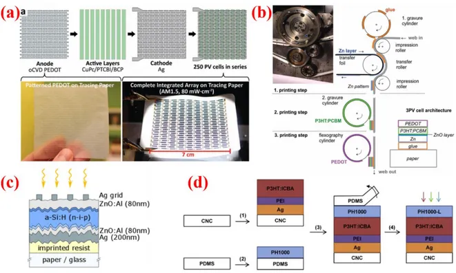
Another strategy consists in gluing a conductive cathode on commercial paper. The layer is transferred from commercial Zn-metallized polypropylene (PP) foils and PP is removed after the transfer. Exposure of the Zn layer in air produces a surface ZnO hole blocking and oxygen barrier layer (Figure 1c). It is possible to pattern paper surface with a cyanoacrylate glue applied by gravure printing before transferring the cathode[9] or to fully cover paper with the Zn/ZnO layer, by gluing the PP side on it. With this second approach, the PP smoothens paper surface and works as a protective layer for the next deposition of active inks.[35]
Covering different kinds of common paper with a transparent anode without previous smoothing treatment is also possible by using PEDOT:PSS (Figure 1d).[50] Deposition is performed by simultaneous exposure to vapor-phase monomer (EDOT) and oxidant (FeCl3) at low substrate temperatures (<100 °C) and moderate vacuum (∼ 0.1 Torr). In situ shadow masking helps to create well defined polymer patterns on paper surface. The evaporated PEDOT:PSS displays mechanical robustness, with unaffected conductivity by several compressive flexing cycles at 5 nm radius.
A pivotal optical property of paper is opacity, essential for reading documents since it avoids interference from print images on the back side of a page. The opacity is a consequence of light scattering in many directions produced by the rough paper surface. However, optical transparency may be a desired property for specific applications: it would enable technological applications in smart windows and smart packaging, and illumination from both sides for light responsive devices such as photodiodes and photovoltaic cells.
13
Infiltration of a transparent plastic, like an epoxy resin, into standard paper pores can increase transparency. The process can be potentially implemented in a roll-to-roll machine for large scale production.[20] The new plastic-paper material possesses a high optical transmittance (> 85%) and a high transmittance haze (> 90%; i.e. ratio between diffused and total light intensity) in a broadband wavelength, enabling enhancement of light coupling through the substrate (Figure 2a). Other approaches based on the same concept are: infiltration of an ionic gel ink, that also confers conductivity to the resulting ionic gel paper,[41] infiltration of carboxymethyl cellulose (CMC),[49] or top coating with green polymerizable deep eutectic solvent (PDES).[40]
Figure 2 a) Concept of plastic-paper production and a photography of the transparency&haze
effect. Reproduced with permission.[20] Copyright 2012, Royal Society of Chemistry. b) Nanopaper (left) and paper (right). Optically transparent paper (left) is composed by 150 nm cellulose nanofibers. The upper left inset, with a scale bar of 100 nm, shows a SEM micrograph
14
of the surface of transparent nanopaper. Conventional cellulose paper (right) is composed by 30 μm pulp fibres. The upper right inset, with a scale bar of 200 μm, shows the SEM micrograph of the surface of a sample of filter paper. Reproduced with permission.[55] Copyright 2009, John Wiley and Sons.
Another route to transparency is given by transparent all-cellulose composites. The fibres are selectively dissolved and swelled by dipping them in a solvent and then re-gathered by compression and drying. This method was applied to filter paper by using N,N-dimethylacetamide as solvent containing LiCl;[52] an alternative is represented by processing the fibres by TEMPO/ NaBr/NaClO oxidation to introduce carboxyl groups onto the cellulose. This weakens the hydrogen bonds between the cellulose fibrils and causes the wood fibres to swell up and collapse resulting in a high packing density and excellent optical properties. The TEMPO oxidised paper can be used as light harvesting enhancing coating in an OPV solar cell.[51]
A striking innovation is given by the use of transparent nanopaper.[55] Nanopaper is composed of nano-dimensioned cellulose crystals and presents high haze and transparency, thanks to the reduced dimension of interstices among nanofibers. The Figure 2b) shows the typical appearance and morphology of filter paper and nanopaper, obtained from 150 nm cellulose nanocrystals (CNCs). The preparation of good quality nanopaper requires procedures taken from the paper industry, including mechanical compression under vacuum and pressures. Nanopaper usually does not need coating layers to be compatible with electronic inks deposition. Some examples of organic and perovskite solar cells deposited on cellulose nanopaper, obtained from tiny nanocrystals or longer (1-2 m) nanofibres, have already appeared on the literature.[56,57,59,61,63,64]
15
Even if nanopaper possesses more appealing optical, mechanical and thermal properties than PET,[19] it still has high costs (0.7-7$ g-1, though it has lower grammage than conventional paper)[75] and is not commercialized, yet; it is mechanically more resistant than standard paper[58] but displays some issues relevant to its highly hygroscopic nature: it swells in water,[61] so it needs some protective treatments to improve its durability in time. Many recent studies have faced the problem proposing protocols for increasing nanopaper stability[65] by hydrophobization [66,67,76] or amphiphobization,[53] or through the formation of crystalline cellulose nanocomposites with cellulose ethers.[70] Some of the strategies were successful and had the potentiality to be applied on large scale production. One limiting aspect connected to the nanopaper or CNCs involvement in new technologies is however still due to the commercial availability of nanofibers and nanocrystals with different length and characteristics, which is, at the moment, still limited.
2.2 Energy storage devices
The characteristic of paper that is considered as a drawback for its implementation in thin film devices, i.e. the rough surface, may represent a desired property in energy storage devices. Paper fibres have up to several tens of m length and 20 m width, and form pores with micro-dimensioned diameter. In energy storage devices paper should act as a flexible and conductive substrate that works as a current collector. Moving in this direction, and conversely from what observed in thin films solar cells, the high porosity enables to exploit the capillary action to absorb active electrode materials. Indeed, the goal here is to get a highly conductive paper that is flexible, mechanically resistant, and highly accessible to ions in the electrolyte. For this goal different approaches have been pursued,[77] mainly based on functionalization with single walled carbon nanotubes (SWCNT) or silver nanowires, [48] graphene,[54] nanoparticles,[43] etc. The characteristic of these coatings lays in their feature to completely cover the cellulose fibres and electrically connect neighbour fibres. This is clearly shown in the Figure 3a-b), for the case
16
of SWCNT: nanotubes are highly conductive and flexible, and they can associate strongly with the cellulose surface and electrically bridge fibres.[48] The final electrode is flexible and it can be prepared by treating the paper with a SWCNT solution. The Figure 3c-d) shows a photography of a SWCNT conductive paper, which is proposed as lightweight and flexible electrode for flexible storage devices in place of a copper foil.[77]
In order to further increase the potential storage of ions/charges it is necessary to increase the surface area. Cellulose nanofibrils networks are ideal nanoporous materials with extremely high content of surface hydroxyl groups that potentially enhances their attitude to self-assembly with the conductive inks. Indeed, a recent work has demonstrated spontaneous association into aggregates of cellulose nanofibers and carbon nanotubes (CNTs) and, more in general, carbon nanomaterials. The close affinity of the two materials allowed the preparation of black CNT-nanopaper, displayed in the Figure 3e).[69] Optical transparency has also been demonstrated for supercapacitors, using nanopaper as substrate. In this case, the transparent reduced graphene oxide (RGO) is used in place of CNTs to enable charge storage: co-deposition of RGO and cellulose nanofibers is allowed by layer-by-layer wet method performed under the assistance of divalent metal ions. Thanks to the close interaction with the cellulose nanofibers, RGO aggregation can be prevented, maximising their potential to store charges.[68]
17
Figure 3. a) SEM micrograph of the SWCNT-conductive paper. The SWNTs are flexible, and
adhere to the fibres surface, eventually bridging over the gaps between paper fibers. b) Higher magnification SEM image revealing the presence of SWCNTs on the fibres surface. Reproduced with permission.[48] Copyright 2009, National Academy of Sciences. c,d) The perspective of replacing thin film conductors, like heavy metal foil, i.e. Cu foil, with conductive paper (d). Reproduced with permission.[77] Copyright 2012, Royal Society of Chemistry. e) CNT functionalized nanopaper. Reproduced with permission.[69] Copyright 2017, American Chemical Society. f) Flexible reduced graphene oxide (RGO)- nanopaper. Reproduced with permission.[68] Copyright 2013, Royal Society of Chemistry.
18
Traditionally, the invention of the printing press is ascribed to Gutenberg in the 15th century. This consisted in the flat-bed type, whilst the rotary one came about in the 19th century. The main medium on which inks were transferred to via printing presses was paper. Printed electronics has been a much more recent development arising mainly towards the end of the 20th century. The main substrates for printed electronics have historically consisted in glass, plastic sheets and metal foils. The development of paper electronics, has seen a surge in interest by research laboratories in more recent years, bringing together the three key fields of “printing”, “paper and “electronics” at the same time. Current deposition techniques for device manufacturing on paper substrates consist mostly of those already utilized for solution processing of these layers on more conventional flexible substrates either for PV,[31,75,78,79] batteries [18,32,33,80,81], supercapacitors, [34] or conductive and semiconducting materials.[82–85]
However, as detailed in Section 2, in the case of light harvesting devices, an overlayer or treatment is usually applied over the surface of paper to improve planarity and printing capabilities of its surface.[11,34] Ink formulation may also be optimized according to the different wetting and adhesion properties of the papers substrates. Differently, the porosity of fibre-based cellulosic substrates may instead be beneficial and exploited for the manufacture of for some types of storage devices as described below.
Currently, spin coating (high control over film thickness but high material waste) still represents the main liquid solution deposition technique utilized in over 50% of the works reviewed in Section 4 for PV devices on paper. Drop casting is also frequently used to deposit active inks on paper substrates, typically when thicker films are required or when wetting issues arise during spin coating. However, drop casting has the drawback of offering very poor control on film thickness. These two techniques are not applicable to high-throughput roll-to-roll industrial scale manufacturing. Interestingly, around 1 in 6 works in the literature employed doctor blade, which is the first step for a more scalable coating, especially when converting this technique in
19
its more sophisticated slot-die form for future industrialization. Slot die coating is a technique where ink is made to go through the interspace in a steel body distributing the ink uniformly over the underlying substrate relatively to which is moved. Respect to doctor blade, it is a technique which gives the possibility of controlling with higher precision the amount of ink used (and wasted) and of obtaining a rectangular patterned film. The rectangular form covers most shapes used in either PV, battery or super-capacitor applications. Other scalable techniques which have been employed for developing PV on paper (see section 4) consisted in screen printing (a non-contact printing technique where the material to be applied is squeezed through a pre-patterned screen mainly used for depositing thicker films, i.e. 510-1 - 5101m), and flexographic printing (where the ink is transferred from a protruding relief on a printing roll, made of rubber or a photopolymer).[75,86] The utilization of spin coating or drop casting for PV cells for the majority of the works published in the literature to date, with no reports on techniques such as slot die or inkjet printing, represents a strong indication that the development of printed solar cells on paper is still well in its infancy along its technology roadmap.
In the case of batteries and supercapacitors (see Section 5), the main means of deposition that have been utilized have been screen printing, and inkjet printing. In general, these are similar to those used for printing PV devices, except for techniques such as impregnation, vacuum filtration and Meyer rod coating. This latter technique is based on the use of a stainless steel rod, wound tightly with a stainless steel wire which is used to doctor off the excess of the coating solution and to control the coating thickness. Stencil printing consists in spreading a paste uniformly over a surface except where stencils block this transfer (i.e they act as masks as well as spacers that determine film thickness). Stencils are made of materials such as metals. These printing techniques are typically used to deposit the electrodes and the electrolyte. It is interesting to point out that the textured and porous consistency of cellulose paper enables the creation also of 3-D electrode systems supported by the substrate. In this case, the conductive
20
materials are embedded in the paper substrates, rather than forming separate layers deposited on their surface. Especially in cases where large thicknesses can be beneficial (e.g. increasing electrodes conductivity or capability to store charges), this strategy has been applied either via soaking, in situ polymerization or vacuum filtration for the manufacture of flexible energy storage devices.[34] The former technique consists in soaking the rough paper substrate in a monomer and carrying out subsequent polymerization (e.g. of a conducting polymer like PANI and PPy). Both the exterior and interior of cellulose fibres become coated with material at the end of the procedure.[34,87] Vacuum filtration is a popular technique for making electrodes rapidly for storage devices and consists in using paper as a “filter” to block materials/particles with sizes larger than the pore size of the paper substrate, exploiting paper’s own intrinsic 3D porous structure.[34] At the end of the process of filtration of the solution containing the material to be deposited (passage of the solution is generally generated by difference in pressure, i.e. vacuum), the surface of fibres and the pores will have been coated with the solid content of the material. The vacuum filtration method has often been used to prepare carbon based (e.g., graphene, graphite, CNT) paper-based electrodes. The challenge for these deposition methods, in which the substrate becomes the electrode, is to be able, at the industrial scale, to generate patterns on a larger paper substrate when wanting to monolithically integrate these with other electronic or non-electronic components. The alternative would be to laminate the devices after their fabrication.
Table 2. Comparison of different large area deposition techniques for printing layers for
PV and energy storage device from inks or pastes. Data collected from references [31–34,83,88]
and the authors’ experience.
Fabrication technique
R2R compatible Material waste Layer thickness accuracy Average Layer thickness (m)
21
Blade coating Y moderate good 10-1 - 5100
Slot die coating Y low very good 10-2 - 100
Spray coating Y moderate/high low 10-1 - 104
Screen printing Y low moderate 510-1 - 5101
InkJet printing y low good 10-2 - 510-1
Flexographic printing Y low moderate 10-2 - 100
Gravure printing y low good 10-2 - 100
Dispenser printing Y low moderate 510-1 - 5102
Stencil Printing Y moderate moderate 100 – 102
Mayer rod printing Y low moderate 100 – 102
Soaking and polymerization
? moderate low
high-depending on substrate and texture
Vacuum filtration ? moderate Low
High-depending on substrate and texture
It can be noted that all the techniques reported in Table 2, except for spin, blade coating, Mayer rod printing, soaking and vacuum filtration, guarantee a print resolution[83] at least in the range of 100-200 microns which is satisfactory for the relatively large-area of the devices covered in this review (i.e. PV and energy storage devices). Rather than printing the films directly in their final form, patterning can occur after coating or deposition of the films. Whereas mechanical scribing is also applicable, laser patterning has become an important tool in the industry of thin film optoelectronics[89] assuring scribing widths below the 100 m range consistently. Scribing by raster scanning laser beam systems thus guarantee a more effective use of space minimizing the dead areas of the devices. Whereas lasers are routinely used when fabricating PV modules on glass and even on PET,[90] application and optimization of its parameters such as wavelength, power, pulse duration, fluence, repetition rates, for patterning printed PV cells on paper requires investigating.
The successful application of large area printing techniques to light harvesting and storage devices not only will enable a seamless integration of these two types of symbiotic devices
22
monolithically on the same substrate, but also the possibility of applying these with other types of printed optoelectronic devices (e.g. transistors, sensors, displays) for the development of paper electronics of the future. As one of the major benefits of paper is its cost, the opportunity of printing electronic devices, rather than utilizing other techniques, can make printed electronics an enabling technology for paper-based applications.
4. Printed Photovoltaic technologies on paper.
In this section, we review the developments of solar cells on paper substrates. We will start by analyzing a critical issue, that of producing effective electrodes, one of which needs to be transparent. We will then cover the literature on the different photovoltaic technologies fabricated on paper in which at least one of the layers has been solution processed. We will conclude this section by describing issues for future development.
4.1. Electrodes
Solar cells are fabricated between two electrodes: i.e. a transparent/window and a back electrode. Commonly used materials for window electrodes are based on transparent conductive oxides (TCO), such as fluorine-doped tin oxide (FTO), indium tin oxide (ITO), indium zinc oxide (IZO), or aluminium-doped zinc oxide (AZO), although in some cases the TCO is replaced by metal grids, metal nanowires, conductive polymers (i.e PEDOT:PSS), carbon nanotubes, 2D materials such as graphene, multilayer stacks of thin metal/dielectrics and a combination of these. [37,91–97] The back electrode usually consists of a thin metallic film i.e. gold (Au), silver (Ag), aluminium (Al) or Platinum (Pt). Most of the solar cells are directly fabricated on a glass/plastic substrate covered with a TCO and the back electrode is deposited on top of the solar cell stack; alternatively, when metal foils are used as substrates[79,98] the window electrode is deposited as the last constituent layer of solar cell. Additionally, the polarity of transparent and back electrode (cathode or anode) can vary depending on the solar
23
cell architecture (i.e direct or inverted, or p-i-n or n-i-p). In order to avoid any confusion and provide a comprehensive overview, we will define bottom and top electrode as the electrode deposited on the substrate or the last layer, respectively, regardless of their transparency or polarity.
As already reported in Section 2, the main challenge in the fabrication of paper based solar cell is the deposition of the bottom electrode on cellulose due to roughness and porosity. [9,59,63,99– 101] In order to produce successful devices deposited on paper, the first active layer, the bottom electrode, needs to be a high quality homogeneous, thin and crack -free layer. Researchers implemented four different methods to deposit bottom electrodes on rough substrates: 1) Optimization of bottom electrode deposition avoiding or exploiting the surface structure,[50,102– 104] 2) modification of the paper surface by using planarization layers,[42,99] 3) use of nanocellulose substrate with smooth surface,[70,101] and 4) development of conductive cellulose substrates.[63] Once the bottom electrode is successfully deposited, the electron/hole transport, active and hole/electron transport layers are deposited following the same procedures used in the control/reference cells on glass or plastic substrates. Finally, the top electrode is mostly deposited by metal evaporation,[35,37] although lamination[62] and sputtering deposition[46,56] are also used.
24
Figure 4. Transmittance spectra of transparent (window) electrodes implemented in solar cells
on cellulose paper substrates. (a) On the left, thickness optimization of evaporated MoOx/Metal/MoOx on PET, with inset data representing the average transmittance TA [%] in the 350-850 nm wavelength range and the sheet resistance ρs [Ω/]; on the right, schematic architecture, energy level diagram, and characteristic J-V curve, with inset picture of a complete device on opaque paper, fabricated with a MoOx/Au/MoOx transparent top electrode. Reproduced with permission.[37] Copyright 2017, IEEE. (b) Nanopaper covered with sputtered ITO, or printed carbon nanotubes (CNT) or Ag nanowires (AgNWs); an organic solar cell, shown in the inset photograph, was fabricated on top of the nanopaper/ITO substrate (bottom electrode) Reproduced with permission.[56] Copyright 2012, Royal Society of Chemistry. (c) Pristine nanofibrillated cellulose (NFC) paper (solid line), and conductive NFC paper (dotted line) obtained by inclusion of AgNWs; the NFC/AgNWs electrode was used as bottom
25
electrode of an organic solar cell ; in the inset, photograph of white opaque printing paper, non conductive NFC and conductive NFC/AgNWs paper substrates Reproduced with permission.[63] Copyright 2015, Nature.
Depending on the cellulose substrate, the transparent (window) electrode is deposited either as bottom or top electrode. Nanocellulose paper allowed the deposition of window electrode without any need of surface treatment thanks to its optical transparency and smooth surface;[70] conversely, in case of an opaque paper substrate the window electrode is deposited on top of the solar cell stack. TCOs including ITO and IZO presented several optical and electrical advantages and have been therefore widely used in paper solar cells.[4,56,70,99,101] ITO is deposited by sputtering in an Argon atmosphere with a high-purity In2O3:SnO2 target. To enhance the electron/hole extraction, a semiconductor buffer layer (i.e ZnO[101]) is coated
between the ITO electrode and active layer. A sputtered ITO electrode was compared with printed silver nanowires (AgNWs) and carbon nanotubes (CNT), as shown in Figure 4b).[56] At 550 nm, ITO delivered a better transmittance:resistivity combination (65%:12/) than CNTs (60%:200/) and AgNWs (78%:25/).
Another transparent electrode commonly used for fabricating solar cells on paper is the dielectric-metal-dielectric (DMD) electrode, consisting in a thin layer of metal sandwiched between two semiconductor oxides. Dielectric layers act as both seeding layers for metal film[37] and as anti-reflection films.[35] The thickness of the metal and its growth (morphology) define the transparency and conductivity of the electrode.[37,57,105] Both n-type and p-type DMD electrodes have been integrated in paper solar cells. N-type (i.e. those that extract electrons) DMD electrodes such as TiOx(40nm)/Ag(10 nm)/TiOx(40nm)[57] or ZnO(40nm)/Ag(12nm)/ZnO(40nm)[106] had a resistance:trasmittance ratio of only 2/:70% (when measured between 400-600 nm) or 7.2/:81.7% (when measured between 400–
26
800nm), respectively. TiOx/Ag/TiOx electrode was used as bottom window electrode on nanopaper for perovskite solar cells (PSC) while ZnO/Ag/ZnO was successfully implemented in organic solar cell. Similarly, p-type DMD presented a good relation between transmittance and sheet resistance. Leonat et al.[35] optimized a MoO3(8nm)/Ag(13nm)/MoO3(25nm) electrode obtaining a sheet resistance of ∼5 /; likewise, Castro-Hermosa et al.[37] studied MoOx/Metal/MoOx electrodes for paper perovskite solar cells, the transmittance spectra of which are shown in Figure 4.a. Although silver increased the conductivity of the electrode, it also allowed UV (wavelength less than 400 nm) transmission which can lead to perovskite degradation[107] as well as possible issues of Ag interacting directly with the perovskite via diffusion or pinholes. On the other hand, the more stable gold increased the electrode transmittance by 10% in relative terms (from 56.4% to 62.5%). Therefore, the final optimized electrode stack consisted of MoOx (17.5nm)/Au(11nm) /MoOx (18.6nm) with TA = 62.5% and ρs = 9/.
A less complex transparent electrode is represented by semi-transparent metal thin films (<25 nm) on their own; however, the solar cell performance is restricted by metal transmittance. [42,59,61,108] Costa et al.[59] deposited 20 nm of Ag on Nano-Crystalline Cellulose (CNC) and
NanoFibrillated Cellulose (NFC) substrates. Organic solar cell
(substrate/Ag/ZnO:Al/PFDTBTP:PC70BM/MoO3/Ag) performance depended on substrate morphology and was lower on NFC than CNC because the higher roughness of NFC induced high series resistance. Additionally, the introduction of a buffer layer as polyethylenimine (PEI) on to the ZnO:Al mixture film led to a reduction of surface roughness and tuned the electrode work function from 4.41 eV to 4.28eV. In a similar work, Zhou et al. [61] modified the Ag surface with a ethoxylated polyethylenimine (PEIE) buffer layer improving the Ag conductivity. Additionally, a transfer lamination of semi-transparent PEDOT:PSS top hole-collecting electrode was developed by Zhou et al. [62] (See Figure 5d). First, PEDOT:PSS (PH1000 with 5 wt% DMSO) was deposited on a PDMS substrate by spin coating (1000 rpm for 30 s) and
27
dried at room temperature for 10 min. Then, the electrode was mechanically sized and transferred on top of the active layer (P3HT:ICBA). Finally, the PDMS was removed. This approach represents a simple vacuum-free deposition process for transparent top electrodes and was necessary to protect the underlying nanopaper substrate and device layers from water solvent, used for PEDOT:PSS deposition. La Notte et al.[109] used a sprayed modified PEDOT:PSS as conductive glue for the application of a composite cellulose/graphene nanoplatelets electrode.[109] Moreover, Barr et al.[50] fabricated a 250-cells organic module presented in Figure 5a) where PEDOT was deposited by vapour printing. The oxidative chemical vapour deposition (oCVD) allowed large area deposition, pattern design and thickness control on any surface including rough and hydrophobic paper. PEDOT:PSS has also been incorporated as top electrode by flexographic printing (Figure 5b).[9] Furthermore, Nogi et al.[63] incorporated the conductive transparent electrode within nanocellulose paper (Figure 4.c). AgNWs (Diameter=50–100 nm, Length=5–10 μm) were incorporated into nanocellulose using three different methods: bar-coating followed by heating or mechanical pressing and drop-casting. The transmittance of the conductive and pristine paper is presented in Figure 4c): paper achieved a favourable transmittance:resistance combination of TA = 91% (at 600nm) and ρs = 34/.
4.1.2. Opaque electrodes
An opaque metal electrode is often deposited on opaque cellulose paper as bottom electrode while on transparent cellulose substrates the opaque back electrode is deposited on top of the device. The most used opaque top electrodes are: MoO3(8-15 nm)/Ag (100-150 nm),[59,61,70] Ca(7nm)/Al(200nm)[56]or Au (80-120nm).[46,57] Metal electrodes provide chemical stability,[37] low cost deposition,[9,35,102,104] light scattering,[110] and high conductivity.[111] Voggu et al.[101] used gold (80nm) as bottom electrode on different commercial papers including standard office
28
paper, photography paper, wax paper and parafilm. With the addition of a chromium (10nm) seeding layer, the growth of gold was enhanced. SEM images of electrodes showed high porosity and discontinuities due to the roughness of paper, and bad adhesion on photography paper was also noted. Then, authors selected a smooth bacterial nanocellulose substrate to prevent interference from these defects in the deposition of gold. Alternatively, several authors reported the use of planarizing layers before metal deposition, in order to decrease the porosity and roughness of cellulose substrates.[42,99] Nevertheless, gold electrodes can present particle-aggregation, which produce rough films.[46] Other metals including thermally evaporated silver,[4,62] solution processed nickel[102,111] and laminated zinc[9,35] have been used in paper solar cells. Hubler et al.[9] reported a roll-to-roll (R2R) printed organic solar cell on the paper substrate described in the Figure 1c), prepared by gravure printing/gluing a zinc foil. The Figure 5b) shows the system of rollers used to modify paper and to glue the zinc foil on it. Gravure printing of glue allowed a selective deposition (patterning) of zinc foil though it and it also could be wet etched with acetic acid.[35] The Zn electrode had ohmic behaviour, a work function of 4.3 eV, low surface roughness (80 nm) and it was deposited in air with a low-cost process. Nickel electrodes deposited by chemical bath reaction at low temperature on paper substrate were used in dye-sensitized solar cell (DSSC) fabrication.[102,111] Nickel electrodes presented better chemical stability than gold when it was immersed in the electrolyte.[102] Characterization of Ni films evidenced a uniform deposition (SEM microscopy) and low resistance (< 1 /, four point probe), which increased when the electrode was annealed.[111] However, metals such as gold,[35] silver and zinc are very hydrophobic[112,113] and lead to poor coverage and inhomogeneous film deposition which would be problematic for the fabrication of printed solar cells. This problem is generally solved with application of UV-ozone surface treatment,[114] use of buffer layers such as polyethylenimine (PEI)[62] or ethoxylated polyethylenimine (PEIE),[35] or metal surface passivation with natives oxides such as ZnO on Zn foil.[9,35]
29
Conductive polymers are a suitable alternative to metal back electrodes for paper solar cells. Poly(3,4-ethylenedioxythiophene): poly(styrenesulfonate) or PEDOT:PSS is widely applied in optoelectronics since it provides satisfactory transmittance and resistance (especially in the vertical direction) behaviour (i.e transmittance:resistivity combination of 85%:25/[115]) and a high work function (useful for the extraction of holes).[116] Moreover, it is solution processable at low temperatures, therefore compatible with R2R printing techniques and paper substrates. For example, PEDOT:PSS doped with dimethylsulfoxide (DMSO) was drop cast on paper resulting in a homogeneous deposition which was independent of substrate hydrophobicity and roughness.[108] Also, Lee et al.[100] coated a commercial A4 paper by immersion in a mixed solution of graphene dots (GD) and PEDOT:PSS (1:1). The resulting electrode was compared with a sputtered Pt electrode as a counter electrode for DSSC (dye-sensitized solar cells), showing an improvement by a factor of 2.9. The incorporation of graphene dots determined a 6-fold increase in conductivity compared to a PEDOT:PSS only electrode. GD:PEDOT:PSS paper electrodes also presented lower resistance and higher flexibility compared to Pt coated cellulose.[100] Anothumakkool et al.[117] reported a PEDOT:PSS electrode deposited using immersion technique. The high conductivity of the electrode (Rs = 4 Ω/□) was attributed to the multi-layer structure of PEDOT. Additionally, the PEDOT electrode was stable for 40 days in air. Besides that, Dasari et al.[104] fabricated a multilayered graphene (MuLG) electrode via a simple H2B pencil scribing. The electrode presented high resistance (5k/cm2) and high roughness. Planarization was achieved by depositing a PEDOT:PSS layer on the surface. Finally, Gao et al. [118] screen printed a carbon electrode (150 um) on cellulose paper exhibiting high roughness and sheet resistance 43 / when measured with four-point probe. Roughness was decreased with a polished process which enhanced the conductivity of electrode reducing the electrode resistance to 14.2 /.
30
Figure 5 Deposition of bottom electrode (a-d) on cellulose paper using different deposition
techniques. (a) Oxidative chemical vapour deposition (oCVD) of PEDOT grid on tracing paper. Organic solar module contained 250 cells. Reproduced with permission.[50] Copyright 2011, John Wiley and Sons. (b) Roll-to-roll (R2R) lamination of Zn electrode on glossy paper, gravure printing of P3HT:PCBM active layer, and flexography of conductive PEDOT top electrode. Reproduced with permission.[9] Copyright 2011, John Wiley and Sons. (c) Paper surface modification with an UV resistive resin. Resin allowed a controllable design of surface pattern which enhanced the light scattering in an a-Si solar cell. Reproduced with permission.[110] Copyright 2017, John Wiley and Sons. (d) Transfer lamination of PEDOT:PSS top electrode. Reproduced with permission.[62] Copyright 2013, Elsevier B.V. All rights reserved.
4.2. Photovoltaic technologies
Photovoltaics can be divided into three main categories: first, second and new generation solar cells.[119] First generation PV is based on mono- and multi-crystalline silicon solar cells, mature
31
technologies with large scale production, that in 2017 accounted for 93.0% of the global annual PV power production.[120] Crystalline silicon devices are characterized by high efficiency and durability but are mechanically vulnerable, and incompatible with cellulose based substrates. Second generation PV include conventional thin-film technologies, such as amorphous silicon (a-Si), copper-indium-selenide (CIS) or copper-indium-gallium-selenide (CIGS), and cadmium telluride.[121] Compared to first generation PV, these devices have reduced thickness (< 10 m), which entails a reduction in materials and manufacturing costs, while maintaining excellent stability in many cases but relative lower efficiencies. Second generation solar cells can be fabricated in flexible form and at lower temperatures, and share 4.5% of the global annual PV power production. Finally, new generation PV include emerging thin-film technologies, such as organic photovoltaics (OPV),[122] dye-sensitized solar cells (DSSC),[123] quantum dots photovoltaics (QDPV)[124] and perovskite solar cells (PSC).[125] Emerging solar technologies are still at a research and development scale, or in some cases recently commercialized on a niche production scale. The main advantages of emerging PV are: solution processability and printability; low cost; potential application on flexible and light-weight substrates; semi-transparency; good performance under normal and diffused incident light and even under indoor lighting.[126,127] However, lifetime (and in most cases efficiencies except for perovskite solar cells where values have exceeded 22%[128] of these devices under standard test conditions is still consistently lower compared to conventional PV.
32
Table 3. Summary of PV devices fabricated on cellulose substrates or including a paper-based component, with at least one layer deposited
by printing techniques.
Technology Substrate Transparent electrode Back electrode Printed layer Printing technique
PCE Area Stability Ref. a:Si:H P_e:smart Type 2 paper IZO (200 nm) (RF magnetron
sputtering) Al (80nm)/ Ag (40 nm) (evaporation) Hydrophilic mesoporous coating Cast-coating 3.40% 0.05 cm2 Stable after 20 cycles 20 mm radius [4] a-Si:H P_e:smart Type 2 paper Ag grid (700 nm) Ag (200nm) /ZnO:Al
(80nm) (RF magnetron sputtering) Hydrophilic mesoporous coating, photoresist Cast-coating, spin-coating 5.50% 0.5 cm2 - [110]
a-Si:H Printing paper ITO (RF magnetron sputtering)/Au grid
Au grid (evaporation) Acrylate lacquer Doctor-blading
6.70% 0.08 cm2
- [99]
CuInSe2 Bacterial nanocellulose paper ZnO/ITO (RF magnetron sputtering) Cr (10 nm)/Au (80 nm) (evaporation) CuInSe2, CdS Spray-coating, chemical bath deposition 2.25% 0.08-0.15 cm2 Stable after 120 bending cycles (5 mm radius); 80% of initial PCE maintained after folding- unfolding [101]
OPV Amylum coated cellulose LiF:Al (30 nm, coevaporation) Au (120 nm, RF magnetron sputtering) PEDOT:PSS, P3HT:PCBM Dipping, spin- coating 0.13% 0.13 cm2 - [46]
OPV NFC ITO (RF magnetron sputtering) Ag (200 nm) (evaporation)
PEDOT:PSS, P3HT:PCBM
Spin-coating 0.21% ND - [56] OPV PE/carton/PE Al (5 nm)/Ag (15 nm) (evaporated) PEDOT:PSS
(drop-casting) PEDOT:PSS, P3HT:PCBM Spin-coating 0.40% 0.18 cm2 - [108]
OPV Glossy paper PEDOT:PSS (flexographic printing) Zn (transfer printing) PEDOT:PSS, Zn, P3HT:PCBM Flexographic, transfer and gravure printing 1.31% (at 60 mW cm2) 0.09 cm2 - [9]
OPV CNC Ag (20 nm) (evaporation) Ag(100nm) (evaporation) ZnO:Al, PEI, PFDTBTP:PCBM Spin-coating 1.40% 0.09 cm2 - [59] OPV CNC Ag (20 nm) (evaporation) Ag (150 nm) (evaporation) PEIE, PBDTTT-C:PCBM Spin-coating 2.70% (95 mW cm2) ND - [61]
OPV NFC Ag nanowires (drop-casting) Al (60 nm) (evaporation) Ag NW, PEDOT:PSS, P3HT:PCBM Drop-casting, spin-coating 3.20% 0.09 cm2
Stable after folding cycles
[63] OPV PET ITO/Ag/ITO (sputtering) Cellulose/Graphene
nanoplatelets (lamination) ZnO, PEIE, PffBT4T:PCBM, V2Ox,PEDOT:PSS Spray-coating 3.36% 0.15-1 cm2 Stable after 100 bending cycles at 7mm radius; 12% PCE decrease after 100 cycles at 4 mm [109]
33 OPV CNC PEDOT:PSS (lamination) Ag (80 nm)
(evaporation)
PEI, P3HT:ICBA Spin-coating 3.80% 0.01-0.06 cm2
- [62]
OPV Printing paper MoO3(8nm)/Ag(13nm)/MoO3(25nm)
(evaporation)
pp-Zn (lamination) PEIE, PTB7:PCBM Spin-coating 4.10% 0.10 cm2
- [35]
OPV Tunicate CNC- O-(2, 3-dihydroxypropyl)cellulose nanocomposites ITO (80 nm) (RF magnetron sputtering) Ag (100 nm) (evaporation) ZnO, PTB7:PCBM Spin-coating 4.98% 0.24 cm2 - [70]
OPV Cellophane ZnO(40 nm)/Ag(12 nm)/ZnO(40 nm) (magnetron sputtering, spin-coating) Al (evaporation) ZnO, PTB7-Th:PC71BM Spin-coating 5.94% 0.06 cm2 92% of initial PCE maintained after 35 folding cycles [106]
OPV Glassa ITO Al (evaporation) PEDOT:PSS,
PCDTBT:PCBM Spin-coating 5.88% (13 mW cm2, diffused) - - [51]
DSSC Box paper Pt-coated glass/FTO Ni (chemical bath) ZnO Doctor-blading
1.21% 0.16 cm2
- [102]
DSSC Box paper Pt-coated glass/FTO Ni (chemical bath) Meso-TiO2 Doctor-blading
2.90% 0.25 cm2
- [111]
DSSC Glassb FTO Pt (evaporation) TiO
2 Drop-casting 3.55% 0.22 cm2 96% of initial PCE maintained after 1000h accelerated aging test [103]
DSSC Glassc FTO Pt (drop-casting) TiO
2, nanocelluose hydrogel, Pt Screen-printing, drop-casting 4.70% 0.40 cm2 90% of initial PCE maintained after 1000h accelerated aging test [129]
DSSC Printing paper ITO/PEN Graphene
dots/PEDOT:PSS (dipping) Meso-TiO 2 Doctor-blading 4.91% 0.16 cm2 Stable after 150 bending cycles [100]
QDPV Glassd FTO FTO TiO2, Pt, CdS
Screen-printing, casting, dipping 0.52% 0.40 cm2 - [130]
QDPV Printing paper Gold-palladium (40 nm) (sputtering)e Multilayered graphene (H2B pencil rubbing) PEDOT:PSS, CdSe QDs:PTCDA:MuLG Spin-coating, drop-casting 1.80% 5.00 cm2 - [104]
PSC PowerCoat HD cellulose MoO
3 (17.5 nm)/ Au (11 nm)/ MoO3 (18.6 nm) (evaporation) Au (80 nm) (evaporation) SnO 2, meso-TiO2, CH 3NH3PbI3, Spiro-MeOTAD Spin-coating 2.70% 0.10 cm2 PCE=0.16% after 72h in air, no encapsulation [37] PSC TEMPO-oxidized cellulose TiO X (40 nm)/Ag (10 nm)/TiOX (40 nm) (sputtering) Au (80nm) (e-beam evaporation) ZnO, CH 3NH3PbI3, Spiro-MeOTAD Spin-coating 6.37% 0.17 cm2 PCE=5.43% after 230h in air, no encapsulation [57] PSC Cellulose Cu(1 nm)/Au(6 nm) (evaporation) Carbon (screen
printing) Carbon Screen-printing 9.05% 0.08 cm2 75% of initial PCE maintained after 1000 bending [118]
34
cycles at 6mm curvature radius a) TEMPO-oxidized cellulose was used as transparent high-haze coating
b) Cellulose-based materials constitute electron transport layer (TiO2-laden paper membrane) and electrolyte (NFC based filler) c) Cellulose-based materials constitute electrolyte membrane (nanocellulose areogel film)
d) Cellulose-based materials constitute filler membrane (NFC, TEMPO-oxidized-NFC) e) Both top and back electrode are opaque
35
4.2.1. Paper-based conventional thin film photovoltaics
Hydrogenated amorphous Silicon
Hydrogenated amorphous silicon (a-Si:H) solar cells are based on a thin (<1 m) intrinsic a-Si film, sandwiched between two heavily doped a-Si regions; the reduced thickness compared to conventional crystalline Silicon, in addition to potential flexibility, make a-Si:H PV a viable alternative for application where light weight and mechanical compliance are required. The first a-Si:H solar cell on a paper substrate was reported by Águas et al.[4] By implementing a printed hydrophilic mesoporous coating to reduce the paper roughness, flexible a-Si:H solar cells with architecture paper/HM/Al (80 nm)/Ag (40 nm)/n-i-p a-Si:H (355 nm)/IZO (200 nm) delivered a power conversion efficiency (PCE) of 3.40% and fill factor (FF) of 40.7%, open-circuit voltage (VOC) of 0.82 V, short- circuit current density (JSC) of 10.19 mA cm−2, under 0.1 W cm -2 AM1.5 conditions. Cells remained fully functional after manual bending at 20 mm radius, due to the flexibility and good adhesion of the different layers of the cell stack on paper.
A substantial improvement in paper-based a-Si:H solar cell performance was reported in the work by Van der Werf et al.[99] The Ag (300 nm)/ZnO:Al (100 nm)/n-i-p a-Si:H (406 nm)/ITO (80 nm)/Au-grid stack was fabricated both on nanoimprinted lacquer-coated paper and stainless steel. The blade-coated nanoimprinted lacquer coating played the dual role of creating a smooth substrate, while reducing at the same time the undesired reflection of the incident light. Interestingly, paper-based solar cells were slightly more efficient than nanoimprinted stainless steel-based devices, mainly due to an increase in VOC (VOC = 897 mV and PCE = 6.7% for paper devices, versus VOC = 811 mV and PCE = 6.5% for stainless steel-based solar cells). This improvement was associated to the lower surface roughness of the lacquer-coated cellulose substrate and to the better texture obtained by nanoimprinting.
36 Copper Indium Selenide
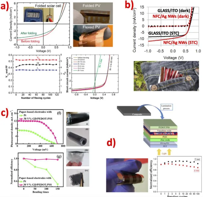
In addition to amorphous silicon devices, another conventional thin film technology has been recently implemented on cellulose substrates, based on spray-deposited CuInSe2 nanocrystals.[101] The bottom contact was a thermally evaporated Cr/Au bilayer on bacterial nanocellulose paper, covered by spray-coating a CuInSe2 nanocrystals ink as the active layer; afterwards, a CdS buffer layer was deposited by chemical bath deposition, and a ZnO/ITO contact thermally evaporated to complete the stack. Flexible cellulose-based devices delivered a PCE as high as 2.25% and a remarkable stability: the efficiency remained unvaried after 120 mechanical flexing cycles at 5 mm bending radius, and the device maintained more than 80% of its initial PCE after folding and unfolding, as depicted in Figure 6.a. The excellent mechanical stability of CuInSe2 paper-based devices is attributed to a stabilization of the top ITO layer determined by the strong adhesion between the active layer nanocrystals and the nanocellulose, that limits the propagation of bending-induced cracks to the top electrode; devices were completely functional after bending at a radius as small as 3 mm.
4.2.2. Paper-based emerging thin film photovoltaics
Organic solar cells
Organic photovoltaic has been the first technology to be transferred from rigid and plastic substrates to cellulose-based substrates. Organic solar cells employ an organic semiconductor (polymer or small molecule), usually sandwiched or blended with a fullerene derivative, to absorb the incident light; after exciton separation, charges are transported and collected at electron and hole selective contacts.[122,131] Being solution-processable and printable, OPV represent a cost-effective alternative to conventional thin film technologies.[132] Even though, in 2005 Lamprecht et al. demonstrated an organic photodiode on a newspaper,[42] it was only in
37
2010 when the first organic solar cell was developed on paper.[46] The device structure consisting in an Au/PEDOT:PSS/P3HT:PCBM/LiF:Al stack fabricated on amylum-coated cellulose delivered a PCE of 0.13% under standard testing conditions (STC, 1 Sun, AM 1.5G, 25°C).
Small improvements were made by employing highly transparent nanopaper prepared from nanofibrillated cellulose (NFC) as a substrate for OPV.[56] The high haze offered by nanopaper was beneficial in terms of light absorption in the active layer. However, solar cells with a device stack composed of NFC/ITO/PEDOT:PSS/P3HT:PCBM/Ca/Al, with the HTL and active layers deposited by spin-coating, only delivered a PCE of 0.21% at STC; the poor efficiency was mainly affected by the low FF determined by the high sheet resistance of the NFC/ITO electrode. The PCE was greatly enhanced by replacing ITO with transparent conductive films of Ag nanowires (NWs).[63] An Ag NWs water suspension and a NFC dispersion were sequentially cast and dried on a silicon wafer; after complete drying, Ag NWs-coated nanofibre paper was obtained.. By printing PEDOT:PSS and P3HT:PCBM layers and evaporating the metallic cathode, a flexible and foldable paper-based solar cell with 3.20% PCE at STC was fabricated; the device was capable of generating power also during and after folding. J-V characteristics and photographs of device are shown in Figure 6.b.