Relationship among current fluctuations during
forming, cell-to-cell variability and reliability in
RRAM arrays
Alessandro Grossi
∗, Cristian Zambelli
∗, Piero Olivo
∗, Enrique Miranda
†, Valeriy Stikanov
‡,
Thomas Schroeder
§,¶, Christian Walczyk
§, and Christian Wenger
§∗Universit`a di Ferrara, Dipartimento di Ingegneria, ENDIF, Via G. Saragat 1, 44122 Ferrara, Italy
†Departament d’Enginyeria Electr´onica, Universitat Aut´onoma de Barcelona, Campus UAB, Cerdanyola del Valles, 08193 Barcelona, Spain
‡IASA, 37 Prospect Peremogy, 03056 Kiev, Ukraine §IHP, Im Technologiepark 25, 15236 Frankfurt (Oder), Germany
¶Brandenburgische Technische Universitt, Konrad-Zuse-Strasse 1, 03046 Cottbus, Germany
E-mail: [email protected]
Abstract—In this work, cells behavior during forming is
moni-tored through an incremental pulse and verify algorithm on 4kbit RRAM arrays. This technique allows recognising different cell behaviors in terms of read-verify current oscillation: the impact of these oscillations on reliability and cell-to-cell variability has been investigated during 1k endurance cycles and 100k pulse stress under a variety of cycling conditions. Conductance histograms for the post-forming current reveal the nanosized nature of the filamentary paths across the dielectric film.
I. INTRODUCTION
Resistive Random Access Memories (RRAM) gathered in-creasing interest in the last few years because of [1]. However, an extensive research activity is still to be performed on this innovative technology in order to increase RRAM reliability and performance: to bring such technology to a maturity level the characterization of array structures is mandatory [2]. RRAM behavior is based on the possibility of electrically modifying the conductance of a Metal-Insulator-Metal (MIM) stack: the Set operation switches the cell into a high conductive state, whereas Reset brings the cell back to a low conductive state. Some technologies require a preliminary forming op-eration to activate such a switching behavior [3]–[6]. Even if such forming process is performed just once, it plays a fundamental role in determining the system performance [6]. A deep understanding of the forming process allows recognising faulty cells from scratch and to get a first glance insight on the cells reliability and performances during lifetime. In this work, cell behavior during forming is monitored through an incremental pulse forming with verify algorithm. Such technique allows recognising different cells behavior during forming in terms of read-verify current oscillations: the impact of these oscillations, interpreted either as the charging of a trap close to the surface of the conductive filament (CF) or the movement of an atom/defect in the filament [7], has been investigated in terms of reliability and cell-to-cell variability
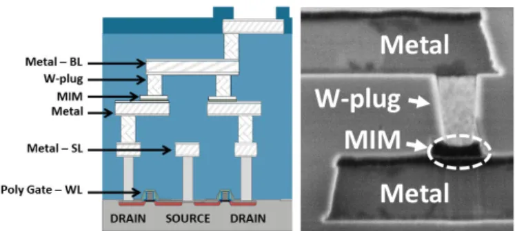
Fig. 1. Schematic and cross-sectional STEM image of the integrated RRAM cell.
during 1k endurance cycles and 100k stress pulses in different cycling conditions.
II. MEMORY ARCHITECTURE ANDEXPERIMENTAL SETUP
The variable resistor of the cells in the 4kbits arrays [8] is a MIM stack composed by 150 nm TiN top and bottom electrode layers deposited by magnetron sputtering, a 10 nm Ti layer, a 9 nm HfO2AVD-deposited layer [3]. The schematic
and cross-sectional SEM image of the integrated RRAM cell including the metal lines and the W based Via-connections is shown in Fig. 1. The resistor area is equal to 1 µm2
. The memory cells are constituted by a select NMOS transistor, which also sets the current compliance, whose drain is in series to the MIM stack connected to the bitlines (BL). Forming operation has been performed using a pulse-verify scheme: a sequence of increasing voltage pulses from 2V to 3.5V with Vstep = 0.01V , Tstep = 10µs is applied on the BL
with a wordline (WL) voltage VW L = 1.4V to set the
forming current compliance and after every pulse a read-verify operation with Vread = 0.2V , Tread = 10µs is performed.
When the read current reaches Itarget = 20µA the forming
operation is stopped. Incremental pulse scheme with verify has © 2015 IEEE. Personal use of this material is permitted. Permission from IEEE must be obtained for all other uses, in any current or future media, including reprinting/republishing this material for advertising or promotional purposes, creating new collective works, for resale or redistribution to servers or lists, or reuse
of any copyrighted component of this work in other works.
This is the accepted version of the paper. The published version can be found at http://ieeexplore.ieee.org/document/7150303/ The DOI of the published version is: 10.1109/IMW.2015.7150303
2.0 2.5 3.0 VFORMING [V] 0 5 10 15 20 25 IREAD [µ A] Forming Threshold Small Osc. G/G0=1 2.0 2.5 3.0 VFORMING [V] 0 5 10 15 20 25 IREAD [µ A] Forming Threshold ∆IREAD Medium Osc. G/G0=1 2.0 2.5 3.0 VFORMING [V] 0 5 10 15 20 25 IREAD [µ A] Forming Threshold ∆IREAD Large Osc. G/G0=1
Fig. 2. Three different behaviors observed during forming process: small (left), medium (centre) and large (right) read-verify current oscillations.
been also implemented for set and reset operations, increasing Vset pulses on the BL and Vreset pulses on the source line
(SL) from 1 V to 3.5 V with Vstep = 0.05V , Tstep = 10µs,
VW L,set= 1.4V , VW L,reset= 2.8V and the same read-verify
condition used in forming. Trise = Tf all = 1µs have been
used on all pulses in order to avoid overshoot issues. Set operation is stopped on a cell when the read-verify current reaches Itarget = 20µA, whereas reset is stopped when
Itarget = 10µA ensuring a minimum resistance ratio of two.
Set and reset BL/SL voltages necessary to reach the requested read-verify current targets are defined as VSET and VRES.
ILRS and IHRS are defined as the read currents measured
after set and reset operations, respectively.
III. EXPERIMENTALRESULTS ANDDISCUSSION Three different behaviors observed during forming process are reported in Fig. 2: while in many cells the read-verify current shows a sudden increase due to the creation of the CF, there are some cells showing read current oscillations with different amplitudes during forming due to the charging of a trap close to the surface of the CF or the movement of an atom/defect in the filament. Oscillations generally appears after reaching the quantum conductance unit G0 = 2e
2
/h corresponding to the creation of a single mode nanowire [9], wheree is the electron charge and h is the Planck’s constant. Fig. 3(a) shows the cumulative distribution of the maximum |∆Iread| measured during forming. ∆Iread is the difference
between two consecutive read verify steps after G/G0 = 1
has been reached, where G = Iread/Vread. The cells have
been arbitrarily gathered in three groups with the same amount of cells defined as follows, as a function of the maximum |∆Iread| oscillation: small (|∆Iread| < 0.5µA), medium
(0.5 ≤ |∆Iread| ≤ 2.2µA) and large (|∆Iread| > 2.2µA).
Fig. 3(b) shows the cumulative distributions of the forming voltages, defined as the voltage required to reach the read-verify targetItarget= 20µA during the incremental pulse and
verify forming scheme. It can be seen that cells with lower forming voltages exhibit smaller current fluctuations.
To evaluate the endurance properties of the cells, 1k cy-cles have been performed through an incremental set/reset procedure: Fig. 4 shows the cumulative distributions of the resistance ratio, set and reset voltages calculated after cycling. Resistance ratio is calculated asILRS/IHRS atVread= 0.2V .
The cells formed with smaller oscillations are shown to require
10-1 100 101 Max(|∆IREAD|) [µA] 0 10 20 30 40 50 60 70 80 90 100 Cumulative Probability [%] Small oscillations
|∆IREAD|<0.5 µA
Medium oscillations
0.5≤|∆IREAD|≤2.2 µA
Large oscillations
|∆IREAD|>2.2 µA
(a) 2.0 2.5 3.0 3.5 VFORM [V] 0 10 20 30 40 50 60 70 80 90 100 Cumulative Probability [%] Small Osc. Medium Osc. Large Osc. (b)
Fig. 3. Cumulative distribution of the maximum read current oscillations measured during forming (a). Cumulative distribution of the forming voltage for the three forming oscillations groups (b).
2 4 6 8
Resistance Ratio (Cycle 1k) 0 20 40 60 80 100 Cumulative Probability [%] Small Osc. Medium Osc. Large Osc. 1.0 1.5 2.0 2.5 3.0 3.5 VSET [V] (Cycle 1k) 0 20 40 60 80 100 Cumulative probability [%] Small Osc. Medium Osc. Large Osc. 1.0 1.5 2.0 2.5 3.0 3.5 VRES [V] (Cycle 1k) 0 20 40 60 80 100 Cumulative probability [%] Small Osc. Medium Osc. Large Osc.
Fig. 4. Resistance ratio, VSET, VRES cumulative distributions for the different forming oscillations groups calculated on cycled devices.
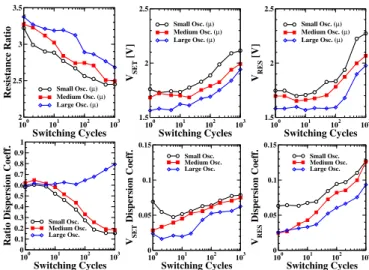
100 101 102 103 Switching Cycles 2 2.5 3 3.5
Resistance Ratio Small Osc. (µ)Medium Osc. (µ) Large Osc. (µ) 100 101 102 103 Switching Cycles 1.5 2 2.5 VSET [V] Small Osc. (µ) Medium Osc. (µ) Large Osc. (µ) 100 101 102 103 Switching Cycles 1.5 2 2.5 VRES [V] Small Osc. (µ) Medium Osc. (µ) Large Osc. (µ) 100 101 102 103 Switching Cycles 0 0.1 0.2 0.3 0.4 0.5 0.6 0.7 0.8 0.9 1
Ratio Dispersion Coeff.
Small Osc. Medium Osc. Large Osc. 100 101 102 103 Switching Cycles 0 0.05 0.1 0.15 VSET Dispersion Coeff. Small Osc. Medium Osc. Large Osc. 100 101 102 103 Switching Cycles 0 0.05 0.1 0.15 VRES Dispersion Coeff. Small Osc. Medium Osc. Large Osc.
Fig. 5. Resistance Ratio, VSET and VRESaverage values and dispersion coefficients calculated during cycling.
higher VSET and VRES after 1k cycles: that means small
oscillations correspond to wider filaments. The Resistance Ratio,VSET,VRESaverage values and dispersion coefficients
calculated during cycling are reported in Fig. 5. To evaluate the cell-to-cell variability the dispersion coefficient of ILRS
and IHRS distributions, defined as (σ2/µ), has been used.
Resistance ratio of cells with large forming oscillations show both higher average value and dispersion coefficient in all cycling conditions: that means large fluctuations correspond to narrower filaments. VSET, VRES average values and
dis-0 5 10 15 20
I
READ [µA] (Small Osc.)
0 20 40 60 80 100 Cumulative Probability [%] HRS Pulse 1 Pulse 1k Pulse 100k 0 5 10 15 20 I
READ [µA] (Large Osc.)
0 20 40 60 80 100 Cumulative Probability [%] HRS Pulse 1 Pulse 1k Pulse 100k
Fig. 6. Cumulative distributions of the read currents (with Vread= 0.2V ) measured during set stress on HRS after different number of disturb pulses, at endurance cycle 1.
5 10 15 20 25 30
I
READ [µA] (Small Osc.)
0 20 40 60 80 100 Cumulative Probability [%] LRS Pulse 1 Pulse 1k Pulse 100k 5 10 15 20 25 30 I
READ [µA] (Large Osc.)
0 20 40 60 80 100 Cumulative Probability [%] LRS Pulse 1 Pulse 1k Pulse 100k
Fig. 7. Cumulative distributions of the read currents (with Vread= 0.2V ) measured during reset stress on LRS after different number of disturb pulses, at endurance cycle 1.
persion coefficients are shown to increase during cycling: switching voltages on cells formed with large oscillations show lower average values and dispersion in all cycling conditions. This indicates cells with lowerVSET,VRES have a not fully
developed filament: this explains the large fluctuations. One reason of the parameters dispersion could be the root mean square surface roughness of HfO2 films due to the columnar
structure of the TiN bottom metal electrode [10].
To evaluate the disturbs immunity of each cells group, 100k reset stress pulses have been applied after set with
Vstress,res = 0.8V , Tstress,res = 10µs and 100k set stress
pulses after reset with Vstress,set = 0.8V ,Tstress,set = 10µs
at different cycles. Set/reset stress voltage pulses with 0.8V have been used since it’s almost half of the average set/reset voltage measured on fresh devices. Cumulative distributions of the read currents measured after reset (HRS), set (LRS) and during set and reset stress on fresh devices are reported in Fig. 6 and Fig. 7, respectively: in both cases cells formed with larger current oscillations show a lower disturb immunity. That reveals larger fluctuations indicate a not so well formed filament thus more prone to exhibit lower immunity.
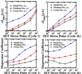
The average current variation and dispersion coefficient calculated on LRS cells during reset stress are shown in Fig. 8: cells with larger current oscillations during forming show a higher variation of the average read current and dispersion coefficient during reset stress in both cycling conditions. Similar consideration can be derived on Fig. 9, showing the
100 101 102 103 104 105
RESET Stress Pulse (Cycle 1)
-3 -2.5 -2 -1.5 -1 -0.5 0 ∆ ILRS [µ A] Small Osc. (µ) Medium Osc. (µ) Large Osc. (µ) 100 101 102 103 104 105
RESET Stress Pulse (Cycle 1k)
-3 -2.5 -2 -1.5 -1 -0.5 0 ∆ ILRS [µ A] Small Osc. (µ) Medium Osc. (µ) Large Osc. (µ) 100 101 102 103 104 105
RESET Stress Pulse (Cycle 1) 0 0.2 0.4 0.6 0.8 Dispersion Coefficient Small Osc. Medium Osc. Large Osc. 100 101 102 103 104 105
RESET Stress Pulse (Cycle 1k)
0 0.1 0.2 0.3 0.4 0.5 Dispersion Coefficient Small Osc. Medium Osc. Large Osc.
Fig. 8. Average read current variation (VREAD = 0.2V ) of LRS and dispersion coefficient evolution calculated during 100k reset pulse stress, with
Vpulse= 0.8V after endurance cycle 1 (left) and 1k (right).
100 101 102 103 104 105 SET Stress Pulse (Cycle 1)
0 1 2 3 4 5 ∆ IHRS [µ A] Small Osc. (µ) Medium Osc. (µ) Large Osc. (µ) 100 101 102 103 104 105 SET Stress Pulse (Cycle 1k)
0 1 2 ∆ I HRS [µ A] Small Osc. (µ) Medium Osc. (µ) Large Osc. (µ) 100 101 102 103 104 105 SET Stress Pulse (Cycle 1) 0.5 1.0 1.5 2.0 2.5 3.0 Dispersion Coefficient Small Osc. Medium Osc. Large Osc. 100 101 102 103 104 105 SET Stress Pulse (Cycle 1k)
0.5 0.6 0.7 0.8 0.9 1.0 Dispersion Coefficient Small Osc. Medium Osc. Large Osc.
Fig. 9. Average read current variation (VREAD = 0.2V ) of HRS and dispersion coefficient evolution calculated during 100k set pulse stress, with
Vpulse= 0.8V after endurance cycle 1 (left) and 1k (right).
average current variation and dispersion coefficient calculated on HRS cells during set stress. Even if after 1k cycles cells show lower sensitivity to set stress due to devices degradation, which means smaller current variation compared to fresh devices, cells with larger current oscillations during forming still show slightly lower disturbs immunity.
To provide a possible physical explanation of the measured phenomenon, Fig. 10 shows the distributions of the read-verify currents measured during forming with medium and large oscillations in units of G0. In order to evaluate only
oscillations observed after the creation of the conductive filament, the analysis has been performed considering only
0.6 0.7 0.8 0.9 1 1.1 1.2 1.3 1.4 G/G0(Medium Osc.) 0.0 0.2 0.4 0.6 0.8 1.0 1.2 1.4 Probability Density Forming Threshold G/G0=1.22 0.6 0.7 0.8 0.9 1.0 1.1 1.2 1.3 1.4 G/G0 (Large Osc.) 0 0.1 0.2 0.3 0.4 0.5 0.6 0.7 0.8 0.9 1 Probability Density Forming Threshold G/G0=1.02 G/G0=1.22
Fig. 10. Distribution of the read-verify current values measured during forming process in units of G0.
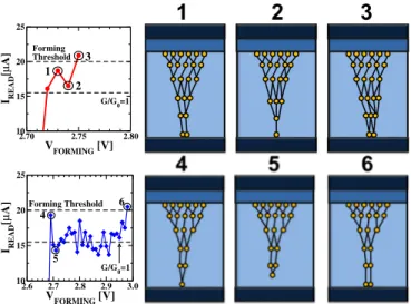
2.70 2.75 2.80 VFORMING [V] 10 15 20 25 IREAD [µ A] Forming Threshold 1 2 G/G0=1 3 2.6 2.7 2.8 2.9 3.0 VFORMING [V] 10 15 20 25 IREAD [µ A] Forming Threshold4 5 G/G0=1 6
Fig. 11. Schematic representation of the CF evolution during medium (1,2,3) and large (4,5,6) read-verify current oscillations.
the read currents values measured in the three verify steps performed after that G/G0 = 1 has been reached. It can be
observed that the distribution of medium read-verify current oscillations shows the highest peak in G/G0=1.22, whereas
large oscillation current distribution shows the highest peak inG/G0=1.02 and the second highest peakG/G0=1.22. This
means that in this case we have two quasi-stable states: the one with the lower conductance corresponds to the narrowest constriction. This is consistent with the current magnitude observed in Fig. 2: the largest fluctuations corresponds to the lower current level in which the filament is formed by only a few atoms and that is why it is very sensitive. A schematic representation of the CF evolution during medium (1,2,3) and large (4,5,6) current oscillations is shown in Fig. 11: a narrow constriction is more prone to exhibit more fluctuations because it is formed by very few atoms/vacancies. Fig. 12 represents the post-forming conductive filaments with different current oscillation properties.
IV. CONCLUSIONS
In this work the relationship between cells behavior during incremental pulse and verify forming algorithm and their performances in terms of endurance, cell-to-cell variability, and disturbs immunity have been investigated. Cells with
Fig. 12. Schematic representation of the post-forming conductive filaments showing different current oscillation properties.
narrowest CF show higher read-verify current oscillations during forming, lower disturbs immunity and higher variability but also better switching properties in terms of set and reset voltages and higher resistance ratio.
ACKNOWLEDGMENTS
This work was supported by the European Union’s H2020 research and innovation programme under grant agreement No 640073.
REFERENCES
[1] S. F. Karg, G. I. Meijer, J. G. Bednorz, C. Rettner, A. G. Schrott, E. A. Joseph, C. H. Lam, M. Janousch, U. Staub, F. La Mattina, S. F. Alvarado, D. Widmer, R. Stutz, U. Drechsler, and D. Caimi, “Transition-metal-oxide-based resistance-change memories,” IBM Journal of Research and Development, vol. 52, no. 4.5, pp. 481–492, 2008.
[2] C. Zambelli, A. Grossi, P. Olivo, D. Walczyk, J. Dabrowski, B. Tillack, T. Schroeder, R. Kraemer, V. Stikanov, and C. Walczyk, “Electrical characterization of read window in ReRAM arrays under different SET/RESET cycling conditions,” in IEEE Int. Memory Workshop (IMW), May 2014, pp. 1–4.
[3] D. Walczyk, T. Bertaud, M. Sowinska, M. Lukosius, M. A. Schubert, A. Fox, D. Wolansky, A. Scheit, M. Fraschke, G. Schoof, C. Wolf, R. Kraemer, B. Tillack, R. Korolevych, V. Stikanov, C. Wenger, T. Schroeder, and C. Walczyk, “Resistive switching behavior in TiN/HfO2/Ti/TiN devices,” in Int. Semiconductor Conf. Dresden-Grenoble (ISCDG), Sept 2012, pp. 143–146.
[4] N. Raghavan, A. Fantini, R. Degraeve, P. Roussel, L. Goux, B. Govore-anu, D. Wouters, G. Groeseneken, and M. Jurczak, “Statistical insight into controlled forming and forming free stacks for HfOx RRAM,” Microelectronic Engineering, vol. 109, pp. 177 – 181, 2013.
[5] C. Chen, H. Shih, C. Wu, C. Lin, P. Chiu, S. Sheu, and F. Chen, “RRAM defect modeling and failure analysis based on march test and a novel squeeze-search scheme,” IEEE Trans. on Computers, vol. 64, no. 99, pp. 1–1, 2014.
[6] P. Lorenzi, R. Rao, and F. Irrera, “Forming kinetics in HfO2-based RRAM cells,” IEEE Trans. on Electron Devices, vol. 60, no. 1, pp. 438–443, 2013.
[7] S. Balatti, S. Ambrogio, A. Cubeta, A. Calderoni, N. Ramaswamy, and D. Ielmini, “Voltage-dependent random telegraph noise (RTN) in HfOx resistive RAM,” in IEEE Int. Reliability Physics Symposium (IRPS), June 2014, pp. MY.4.1–MY.4.6.
[8] C. Zambelli, A. Grossi, D. Walczyk, T. Bertaud, B. Tillack, T. Schroeder, V. Stikanov, P. Olivo, and C. Walczyk, “Statistical analysis of resistive switching characteristics in ReRAM test arrays,” in IEEE Int. Conf. on Microelectronics Test Structures (ICMTS), Mar 2014, pp. 27–31. [9] E. Miranda, C. Walczyk, C. Wenger, and T. Schroeder, “Model for
the resistive switching effect in HfO2 MIM structures based on the transmission properties of narrow constrictions,” IEEE Electron Device Letters, vol. 31, no. 6, pp. 609–611, 2010.
[10] P.-S. Chen, Y.-S. Chen, H.-Y. Lee, T.-Y. Wu, P.-Y. Gu, F. Chen, and M.-J. Tsai, “Impact of flattened TiN electrode on the memory performance of HfO2based resistive memory,” Electrochem. and Solid-State Letters, vol. 15, no. 4, pp. H136–H139, 2012.