RICERCA DI SISTEMA ELETTRICO
Photon harvesting from nanostructured metallo-dielectric substrates
F. Buatier de Mongeot, C. Martella, M.C. Giordano, C. Mennucci
P. Delli Veneri, L.V. Mercaldo, I. Usatii, E. Esposito
Report RdS/2012/212
Agenzia nazionale per le nuove tecnologie, l’energia e lo sviluppo economico sostenibile
“PHOTON HARVESTING FROM NANOSTRUCTURED METALLO-DIELECTRIC SUBSTRATES”
F. Buatier de Mongeot, C. Martella, M.C. Giordano, C. Mennucci (Università di Genova, Dipartimento di Fisica)
P. Delli Veneri, L.V. Mercaldo, I. Usatii, E. Esposito (ENEA)
Settembre 2012
Report Ricerca di Sistema Elettrico
Accordo di Programma Ministero dello Sviluppo Economico - ENEA Area: Produzione e fonti energetiche
Progetto: Sviluppo di tecnologie avanzate per componenti fotovoltaici innovativi
Indice
Abstract……… ………4
Introduction ... 5
Text body – Description of the activity and results ... 6
2.1 Light-trapping via nanopatterning of glass and TCO interfaces ... 6
2.2 Patterning of Si and GaAs interfaces : antireflection and Haze functionality ... 11
2.3 Transparent metal nanoelectrodes with plasmonic functionality ... 16
Conclusions ... 17
Abstract
This report describes the results of the research collaboration between ENEA-Centro Ricerca di Portici and the Department of Phyiscs of the University of Genova (DIFI) developed in the course of 2011-12 within the MSE-ENEA protocol. The main goals of the research are related to the synthesis of nanopatterned substrates in view of Photon Harvesting applications in thin film photovoltaic devices. The activity has been mainly focused on the optimisation of the self-organised nanopatterning processes employed to prepare textured interfaces endowed with high aspect ratio nanostructures The activity was in particular oriented at the synthesis of anisotropic self-organised gratings on substrates of relevance for thin film PV applications such as Glass and transparent conductive oxides (TCOs). The nanoscale morphology has been optimised in view of (i) a broadband reduction of the reflection losses, mimicking the bio-mimtetic interfaces at the cornea of nocturnal moths, and (ii) a high scattering efficiency at large angles in order to greatly increase the Haze of the interfaces (the ratio of diffuse to total scattering). This result has been achieved recurring to a process based on defocused Ion Beam Sputtering (IBS) which employs a self-organised array of metal nanowires as a stencil mask for Ion Projection Lithography (IPL). Of relevance for future applied developments, the process is able to produce a pattern across macroscopic portions of the substrates in a single maskless step, and can be up-scaled into standard industrial coaters. The nanopatterned substrates have subsequently been employed by ENEA as supports for a:Si thin film solar cells, which have succesfully demonstrated a significant enhancement of EQE, in the order of 20%, with respect to the flat reference substrates.
The general validity of the results has been demonstrated by performing similar experiments on bulk semiconductor substrates of interest in photovoltaic applications, namely on Si and GaAs wafers. Also in this case the patterned substrates exhibit a significant broadband reduction of the reflection and a remarkable increase of Haze well above 50%.
The experiment performed in Genova have also demonstrated that the self-organised nanowire arrays employed as stencil masks in the IBS process, perform as semitransparent nano-electrodes with an extremely low sheet resistance in the 1 Ohm/sq. ram. This feature together with the high optical transparency, renders the metal nanowire arrays competitive with the best conventional TCOs. Additionally the nanoelectrodes support localised Plasmon resonances which make them appealing in view of photon harvesting applications in photonic devices and in biosensors.
Introduction
In conventional thick Si solar cells, light trapping is typically achieved using a pyramidal surface texture in the range of several micrometers that causes scattering of light into the solar cell over a large angular range, thereby increasing the effective length of the photon path [1-3]. Such large-scale geometries are not suitable for thin-film cells, for geometrical reasons (as the surface roughness would exceed the film thickness) and because the greater surface area increases minority carrier recombination in the surface and junction regions.
There has been substantial progress in the engineering of structures to enhance photocurrent in thin film solar cells, but there are few comprehensive studies which provide general and intuitive insight into the problem of light trapping and photon harvesting, which is the core of this collaborative research effort. Photo current enhancement in thin film solar cells has been e.g. attempted recurring to periodic and random interface textures either at the front electrode [4] or at the backreflector [5].
On one side, an experimental top-down method capable of implementing arbitrarily designed surface morphologies directly into functional devices is desirable for obtaining broad-band light trapping at multiple incidence angles. On the other side low cost, self-organised techniques capable of patterning large substrate areas are intensely searched in view of large scale applications. This last issue is the core of the activity of the UNIGE unit which has developed original self-organised nanopatterning techniques based on defocused ion beam sputtering to prepare nanostructured supports for thin film solar cells featuring enhanced light trapping.
In brief we have optimised our nanopatternig approaches in view of the following functional applications:
(i) Light-trapping from textured interfaces: A promising route proposed for achieving light trapping in thin-film solar cells is the use of textured interfaces with very high Haze (ratio of diffuse to specular scattering ). The submicrometer lateral periodicity coupled to the high aspect ratio of the nanostructures results in efficient light scattering at large angles [4,5].
(ii) Anti-reflective Bio-mimetic texturing: A further gain can be achieved from the reduction of the reflection losses at the various interfaces if high aspect ratio structures with non diffractive subwavelength periodicity are formed, in a way that the morphology mimics the bio-mimetic texture of the eye of nocturnal moths [6], providing a smooth variation of the refractive index.
(iii) Light scattering and near-field amplification from plasmonic nanostructures: An alternative route which has been proposed to harvest light in thin film devices, employs metallic nanostructures that support localised surface plasmons, excitations of the conduction electrons at the interface between a metal and a dielectric. By proper engineering of these metallo-dielectric structures, either located at the back and front surface, light can be concentrated and ‘folded' into a thin semiconductor layer, thereby increasing the absorption [7].
(iv) Metal nanowire electrodes as alternative to Transparent Conductive Oxides (TCOs): The final issue regards the development of functionalised TCOs doped with metallic nanoparticles and nanowires, in order to enhance electrical transport at comparable transparency and with processing temperatures near room T, in order to be compatible with flexible polymer substrates [8].
High throughput parallel and self-organised approaches for the growth of functional nanostructures are intensely studied as a promising alternative to the cumbersome top-down methods [9-12] or to chemical methods [11-13]. For these reasons alternative approaches based on the physical synthesis of textured substrates and of laterally ordered arrays of metal nanoparticles are actively investigated.
2 - Text body – Description of the activity and results
2.1 Light-trapping via nanopatterning of glass and TCO interfaces
Thin-film solar cells based on amorphous silicon represent a well established technology for cost effective and large scale production of solar cells. Unfortunately, in order to achieve reasonable photon conversion efficiency in thin film solar cells innovative technical breakthroughs are needed. In fact the thickness of the active layers provide a poor absorption of large wavelength photons since the semiconductor absorption length exceeds the thin film thickness significantly. Furthermore, the high refractive index of amorphous silicon is responsible for the strong losses due to reflection at the material interface.
In several promising approaches these limitations are addressed by using textured interfaces, both in the front transparent conductive oxide (TCO) layer, and in the back contact of the photovoltaic devices. Such texturing can induce enhanced light trapping due to different effects. When the characteristic lateral dimension of the surface features is smaller than light wavelength and the vertical amplitude is of the order of a significant fraction of light wavelength, light travels through an effective medium in which the refraction index progressively changes from that of air to the value of the surrounding to the material (grading index effect) [14]. This smooth gradient of the refractive index allows to reduce the reflection losses at the interface over a broad spectral range and mimics the behaviour of the corneas of nocturnal moths [6]. Furthermore, surface roughness with lateral dimension comparable or bigger than light wavelength allows to diffract light at high angles, thus increasing the optical path of photons across the active layer and consequently enhancing photon absorption. In some cases, one or more of these diffracted orders can be resonant with waveguide modes in the active layer thus resulting in a significant enhancement of photon absorption [5]
Huge efforts are now made in order to identify the optimal geometry of the texturing (amplitude and wavelength) which allows to maximise antireflection behaviour and light trapping [4]. Furthermore, nanopatterning techniques that fulfil large scale and cost effective production are required. Wet chemical etching, with or without a sacrificial mask, is a simple and low cost approach to realize random texturing on a broad range of surface materials. However the characteristics of the texturing are strongly affected by the structural/chemical properties and quality of the surface itself thus making difficult to texture interfaces with controlled optical properties. Other approaches based on photolithography allow to control all the geometrical parameters of the surface nanostructures thus preparing one or two dimensional gratings with a lateral resolution on a scale of few tens of nanometers. Unfortunately these techniques cannot fulfil the requirements of large scale and low cost production and for these reasons, methods based on self-organised processes of the surface appear particularly appealing.
In refs. [15,16] we have recently demonstrated that, recurring to Ion Beam Sputtering, a polycrystalline gold film can be transformed into an array of nanowires which acts as a stencil mask for Ion Projection Lithography (IBS-IPL). In this way it is possible to guide the formation of high aspect ratio surface features on supporting substrate materials that are of primary importance for solar technology, such as glass and GaAs.
In this work the stencil masks have been grown on glass and Al-doped ZnO (AZO) supporting substrates in order to obtain high aspect ratio textures at the surface of a TCO of great relevance for photovoltaic applications. Additionally, we have studied the effect on the pattern formation process of a 1-nm thick titanium adhesion layer between the AZO/gold interface. The textured TCO interfaces have been characterized recurring to optical reflectivity measurements in order to evidence (i) anti-reflection behavior induced by the subwavelength surface features (grading index effect) and (ii) the enhanced scattering of light in diffracted orders, by large scale surface undulations. The most promising textured substrates have been subsequently tested by ENEA as supports for a:Si thin film solar cells, demonstrating successfully that light trapping leads to significant increase of the absorbed photocurrent [17,18].
Methods
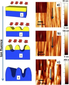
The sacrificial metal mask employed for the pattern transfer process is formed from a 150 nm polycrystalline Au film which has been deposited by thermal evaporation both on the bare and on the titanium precovered Al:ZnO film (AZO). The AZO film was prepared in an UHV chamber equipped with an RF Magnetron Sputtering system (MAK source, Meivac Inc.) from a 2” ceramic target (ZnO/Al2O3 98:2 wt%, 99.99% pure). The base pressure in the chamber was 8.0 x 10⁻⁶ mbar and the sputtering pressure was controlled in the range 2.0-4.0 x 10⁻³ mbar introducing high purity argon gas. Substrates were placed parallel to the target surface at a distance of 4.5 cm and the RF power was fixed at 150 Watt. The AZO films employed for the tests of the a:Si thin film solar cell were grown by ENEA in an equivalent RF Magnetron Sputtering facility. Thickness of the gold film has been monitored by means of a calibrated quartz microbalance. The metal films have been exposed to defocused ion beam irradiation from a gridded multiaperture Ar+ source (Tectra instruments) under grazing incidence conditions (θ=82°) at a constant flux of 4.0 × 10¹⁵ ions/cm-2 s-1 (measured in a plane orthogonal to the beam direction) and an energy of 800 eV. A biased tungsten filament (V bias = −13 V), providing electrons via thermoionic emission, was placed close to the extraction grid in order to compensate surface charging effects due to ion irradiation. As reported in refs. [15,16] during the first stages of the ion bombardment, the sacrificial metal film self-organises into a nanowire array, which at higher ion fluencies performs like a lithographic stencil mask that guides etching of the underlying substrate propagating and amplifying the mask pattern. Prolonging ion irradiation until the complete removal of the residual gold, an anisotropic self-organized pattern, made by corrugations running parallel to the ion beam projection, is effectively formed on the AZO substrates. The process is schematically sketched in Figure 1, where numbers help the reader to follow the chronology of the pattern transfer mechanism.
The morphology of the samples was investigated ex-situ by means of atomic force microscopy (AFM) operating in intermittent-contact mode (Nanosurf Mobile S) equipped with a high aspect ratio Si tip ( ACLA by AppNano). The topography images have been processed recurring to WSxM software in order to evaluate the root-mean-square (rms) roughness σ and other statistical parameters of the patterns.
Optical characterization of the sample’s was made by means of a compensated deuterium-halogen lamp (DH-2000-BAL, Mikropak) coupled though an optical fiber system to an integrating sphere (Ocean Optics
Figure 1: Skecth of the pattern transfer mechanism. AFM topography: a)gold metallic mask; b) Al doped
ZnO substrate patterned by IBS with titanium wetting layer; c) Al doped ZnO film deposited on pre-patterned glass. Reader has to notice the different in plane scale bar of panel a), b) and c). Blue arrows
ISP-50-8-R) whose output was processed by a PC controlled high resolution solid state spectrometer (HR4000, Ocean Optics) .
Results: Pattern formation
In Figure 1 (a) we show the topography of the metallic stencil mask employed in the IBS-IPL pattern transfer process. The AFM topography of the AZO sample patterned by IBS-IPL using the stencil mask of samples is shown in Figure 1 (b). From a visual inspection one can notice that the morphology of the AZO substrate reproduces well the morphology of the metallic stencil mask, and the anisotropy of the pattern is clearly highlighted by the self-correlation images reported in the insets. In agreement with the results of refs. [15,16], the surface undulations of the stencil mask running parallel to the ion beam projection (blue arrows) are transferred to the substrate with an amplified vertical dynamic.
For the AZO substrate without Ti adhesion layer (data not shown) the pattern after erosion of the stencil mask is qualitatively comparable to that of Figure 1(b) apart from a small increasing of the superficial roughness. This is made clear by comparison of the RMS roughness σ of the patterned substrates with that of the metallic stencil mask. For the latter the rms roughness value is around 11 nm, conversely for the topography of Figure 1(b) we measured =25 nm (to be compared with the AZO substrate without the Ti layer for which reads 30 nm). Correspondingly the vertical range (z-axis) extends well above 130 nm in both cases. It must be also evidenced that during the pattern transfer process there is a coarsening of the small scale lateral modulations which are propagated in the AZO films with reduced efficiency.
In Figure 1(c) we finally plot the AFM topography of an AZO film grown on a pre-patterned glass substrate prepared by IBS-IPL using an Au stencil mask whose life has been extended by co-deposition from an auxiliary metal source. In this way it is possible to increase significantly the vertical dynamic range of the glass template and correspondingly the corrugations of the supported AZO film extend up to 400 nm, with a σ value around 67 nm. Visual comparison of the AFM patterns in Fig.1(a) and 1(c) allows to directly conclude that a significant coarsening of the smaller scale spatial features has taken place during AZO deposition.
Optical characterisation
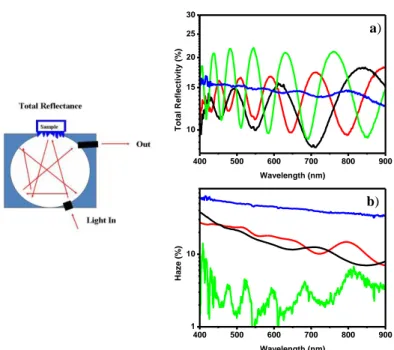
Optical measurements have been made by means of an integrating sphere setup as sketched in the inset of Figure 2 (a): light is fibre coupled to the sphere and propagates at an incidence angle of 8° with respect to the substrate normal. In Figure 2 we compare the measured total reflectance spectra of the patterned AZO substrates with and without Ti wetting layer (black and red trace respectively), of the AZO film deposited on the templated glass (blue trace) and of a flat reference AZO substrate (green trace). Due to the small film thickness, interference phenomena take place at the interfaces as evidenced by the fringes in the spectra. The amplitude of the oscillation is progressively reduced as the surface roughness increases and the fringes disappear for AZO film grown on a pre-patterned glass.
The antireflection behavior induced by the sub-wavelength texture can be evaluated comparing the area subtended by the curves in the spectral range 400-900 nm to that of an unpatterned substrate. This comparison reveals that a reduction of the reflectivity with respect to the flat film is obtained for all the textured samples. For the AZO substrates obtained with the pattern transfer mechanism, the reflection losses are reduced in the range 9-13%, with the best performance measured for the sample with the Ti adhesion layer. In the case of the AZO film deposited on the patterned glass the anti-reflection behavior instead shows a smaller reduction of the reflectivity in the range of 4%.
As discussed previously the effect of surface texturing is appealing since features with lateral scale of the order of the optical wavelength are responsible for the redistribution of the reflected intensity from the specular components to diffracted orders at large angles. This enhancement of light scattering is of primary importance in order to achieve efficient light trapping in thin film solar cells. We thus evidenced the scattering properties of the textured substrates by excluding the specular component of the reflected beam in the optical measurements performed with the integrating sphere.
400 500 600 700 800 900 10 15 20 25 30 T o ta l R e fle c tiv it y ( % ) Wavelength (nm) a) 400 500 600 700 800 900 1 10 H a z e ( % ) Wavelength (nm) b)
Figure 2 a) Total reflected light measured by means of an integrating sphere setup as sketched in the inset.
b) Ratio between diffuse and total reflected light: haze function. Green trace refers to flat AZO film, red and black traces refer respectively to patterned substrate with and without titanium wetting layer, blue trace to
AZO film grown on patterned glass.
In Fig 2 (b) we plot the ratios between the diffuse and total reflected light (Haze); in order to evidence more clearly the trend of the traces, we performed a smoothing over the characteristic period of the oscillations. We can observe that Haze is strongly enhanced over the entire spectral range for the patterned TCOs with respect to the reference flat substrates (green trace). Both AZO samples supported on flat glass (with and without TI ) textured with the pattern transfer mechanism have Haze of about 20% for wavelengths smaller than 600 nm and 10% for longer wavelengths. Haze function for the sample obtained without the wetting layer (red trace) is higher than the sample with the wetting layer (black trace) almost everywhere in the considered spectral range.
An extraordinary amplification of the Haze function is instead observed for the AZO film deposited on the pre-patterned glass: in this case the Haze is above 50% for wavelength shorter than 600 nm and rapidly decreases towards 40% for longer wavelengths. In the case of the flat TCO (green trace), Haze remains throughout the considered wavelength range in the % range; the non zero value is mainly related to an instrumental artefact since the specular beam component is not completely captured by the light trap.
Discussion
In order to the better understand the observed optical behavior we now correlate it with a quantitative analysis of the morphological changes. In Figure 3 we plot the 1-dimensional power spectral density functions g(q) corresponding to the AFM topographies of Figure 1 (c)-(d). The g(q) functions have been averaged over the rows of several AFM images. The analysis of these functions helps to clarify the role of the Ti adhesion layer in the roughening process of the AZO substrates. One can notice that for wavevectors
q>2*10-6, corresponding to corrugations with spatial wavelength λ=1/q smaller than 500 nm, the g(q)
functions are quantitatively the same and the role of the titanium wetting layer in this case is negligible. Furthermore the g(q) functions follow a linear trend in the log-log plot compatible with the power law q-4, a clear indication that relaxation of the surface profile is dominated by diffusive mechanism in both cases. For smaller wavevectors things are different: an amplification of the corrugations with lateral spatial dimension larger than 500 nm is observed in the absence of the Ti adhesion layer. This means that ion induced roughening of the surface on the lateral scale bigger than 500 nm is counteracted by the titanium adhesion layer which prevents de-wetting mechanism of the metallic mask. The morphological
observations can be easily linked with the measured optical properties. The presence of amplified surface 10-3 10-2 105 106 107 108 109 1010 1D -PSD g (q) q(1/nm)
q
-4Figure 3 Log-log plot of 1D-PSD functions g(q) averaged over several AFM topographies. On the left of the
plot and from top to bottom: patterned glass used as template for the TCO deposition (gray trace), deposited AZO film on patterned glass (blue trace), AZO substrate patterned by IBS without wetting layer (red trace), AZO substrate patterned by IBS with wetting layer (black trace). The dot-dashed black trace correspond to a q-4 power law trend.
features with lateral dimensions larger than 500 nm is in fact responsible for the enhanced light scattering observed in the sample without the titanium layer (Figure 2) since light scattering is more effective for wavelengths smaller than the characteristic scale of the surface features.
For the AZO samples grown on textured glass substrates pre-patterned by similar stencil masks, we observe a strong increase of the Haze above 50% due to the amplification of the large scale spatial features [17]. The small scale features, responsible for the moth-eye antireflection functionality, are instead reduced in amplitude since the glass pre-patterning process is performed at high temperatures for which diffusive relaxation is more efficient at the smaller length scales.
Tests on solar cells
In order to test the potentiality of the nanostructured glass substrates in view of photon harvesting applications, we have grown two identical thin film amorphous Silicon p-i-n single junction solar cells supported on patterned and flat templates. The TCO layers (AZO) were deposited by ENEA recurring to RF-magnetron sputtering. The growth of the transparent oxide layers proceeds conformally on the glass
400 500 600 700 800 0,0 0,2 0,4 0,6 0,8 1,0 Patterned glass Flat glass E Q E Wavelength (nm)
nanostructured (blue circles) and flat (red circles) glass substrate. The line is guide for the eyes.
substrates, and results in a film characterized by high optical transmission (about 80%) and low sheet resistance (≈10 Ω/sq). The p-i-n structure grown by ENEA consist of a 7 nm-thick amorphous silicon-carbide p-layer, a 350 nm-thick amorphous silicon i-layer, and a 30 nm-thick microcrystalline silicon n-layer deposited by Plasma-Enhanced Chemical Vapor Deposition (PE-CVD) . From the I-V characteristic similar values of Fill Factor (about 60%) and open circuit voltage (about 0.8 V) have been obtained with both substrates. The short-circuit current density (JSC) of the solar cells has been calculated from the EQE curves by convolution with the photon flux of the global air mass 1.5 (AM1.5g) solar spectrum. The comparison between the spectral responses measured with the two substrates, shown in Figure 4 demonstrates that the EQE of the cell grown on the nanopatterned substrate is higher in comparison to that of the flat reference substrate over the whole spectral range, in particular for wavelengths approximately above 430 nm. The significant enhancement of EQE, in the order of 20%, indicates a corresponding increase in photocurrent with respect to the flat substrate, while the reduction of the fringes caused by interference phenomena is due to scattering from the uncorrelated roughness of the patterned substrate. JSC increases from about 12 mA/cm2 evaluated for the flat glass to about 14 mA/cm2 for the nanostructured one. In particular, the significant EQE improvement in the long wavelength range is indicative of efficient light trapping achieved thanks to the substrate texturing, that determines multiple passes of scattered light within the solar cell. Furthermore, the 1-dimensional periodicity of the glass pattern, which is conformally replicated in the other high refractive index layers constituting the solar cell, provides favourable conditions for trapping of the higher diffracted orders in waveguided modes, both in silicon and ZnO:Al layer [19]. All these effects in combination with the reduction of the reflection losses at interfaces are expected to contribute to the overall enhancement of the photon conversion efficiency of the device.
2.2 Patterning of Si and GaAs interfaces : antireflection and Haze functionality
Here, following the approach described in the previous paragraph, we exploit the possibility to produce high aspect ratio nano-patterns on bulk semiconductor substrates of relevance for photovoltaic applications such as Si and GaAs[20]. We then exploit the patterned substrates with the aim of tailoring their specular and diffuse surface reflectivity and haze as a function of ion fluence. These experiments are optimized in view of photon harvesting applications exploiting the moth-eye functionality coupled to the high scattering efficiency of the surface morphology. The general validity of the approach is further demonstrated by comparison of the experiments on GaAs with those on Si substrates, another material of relevance for photovoltaic and photonic applications.
GaAs: Morphological analysis
The main purpose of this work is to investigate the possibility to employ IBS in the pattern transfer version as a nanostructuring technique of a material's surface for the realization of functionalized interfaces in view of photon harvesting in solar cells. For this reason we decided to use GaAs substrates due to their relevance in the field of electronics and optics applications. On the other hand, it is well known that a GaAs surface is not prone to develop a self-organized pattern if directly irradiated by a low energy ion beam. Up to now, few experimental observations of ripple formations on a GaAs surface by IBS are reported and differences with respect to our case regard ion species ( i.e. heavy Cs+ , reactive O 2+ ) [21] and energy (60 keV with Ar + ion beam) [22]. On the other hand dense arrays of dots have been formed with a low energy (0.7-1 keV) Ar + ion beam [23] at normal incidence and substrate temperature of 180°C.
A polycrystalline (150 nm thick) Au film was deposited by physical vapour deposition (PVD) on GaAs substrate and exposed to a defocused Ar+ ion beam at grazing angle incidence (=82°). Under ion irradiation the surface of the polycrystalline metal film develops a rippled morphology with ridges running parallel to the beam projection [24]. By increasing ion fluence the valleys of the ripple modulation reach the substrate so that the pattern decomposes into a well disconnected nanowire array. In Fig. 2.1(a) we show a 6 µm × 6µm AFM topography of the Au surface at a fluence F1 = 33 1017 ions/cm2, which clearly
evidences the formation of a nanowire array pattern elongated along the ion beam direction (black arrow). 1μm 1μm
(a)
(b)
1μm(c)
(d)
1μm 100 1000 1E-17 1E-16 1E-15 1E-14 H cf (r) (m 2 ) r (nm)T
Figure 2.1: AFM topography images of (a) Au/GaAs surface sputtered at =82° and fluence F1 = 3.3 1018
ions/cm2, (b) GaAs surface sputtered at =82° and fluence F2 = 4.9 1018 ions/cm2, (c) GaAs surface sputtered at =82° and fluence F3 = 3.49 1019 ions/cm2. Black arrows: projection of the ion beam along the substrate
plane. (d) Log-Log plot of the height-height correlation functions H(r) = <(h(x+r)-h(x))2>.
As reported in Ref. [15] and [16] this is the typical dose at which the Secondary Neutral Mass Spectra (SNMS) reveal an increase of the signal originating from the substrate material and a concurrent decrease of the Au signal, once the deepest metallic grooves have reached for the first time the substrate (disconnection of the metallic ripple pattern). Prolonging the ion dose the GaAs begins to become locally eroded, thus transferring the pattern to the substrate, and at fluence F2 = 4.9 1018 ions/cm2 the metallic mask is completely removed, Fig. 2.1 (b). The evolution of the surface morphology further exposed up to a fluence F3 = 3.49 1019 ions/cm2 is shown in Fig. 2.1 (c).
A first quantitative indication of the nanostructuring process is given by the roughness analysis of the AFM images. In agreement with results reported in Ref. [15], in the case of the pattern transfer from Au to glass substrate, an extraordinary vertical amplification of the superficial corrugations is observed in the transmitted pattern. Performing a quantitative analysis of the AFM images [25] we measure a rms roughness almost four times higher for the sample sputtered at fluence F2 ( ~ 45 nm) with respect to the metal film ( ~ 12 nm). This evidences that during the pattern transfer process, ion beam erosion takes place with two different velocities at the exposed GaAs substrate in middle of the grooves and at the residual gold on top of the ripple crests. During the disconnection stage, the GaAs system is forced into a strongly out of equilibrium morphology by the Au mask, so that the evolution of the surface pattern is the result of the competition between the local erosion action of the ion beam, imposed by the anisotropy of the patterned metallic mask, and the smoothing effect of GaAs related to efficient atom diffusion [16]. Exposing the system up to F3 fluence a dramatic drop of the roughness down to ~16 nm is observed: once the perturbing action of metallic mask has been removed, the GaAs surface tends to relax and smoothing mechanisms prevail over ion induced roughening, due to enhanced Ga mobility (preferential Ga enrichment, thermal and ion -enhanced diffusion, viscous flow relaxation) [16].
Observing the AFM images one can notice that, on the surface of the GaAs substrates, a self-organized pattern is formed similar to that on the metal film but changes are also evident in the lateral
dimension of the corrugations when increasing ion fluence. Fig. 2.1(c), for example, demonstrates that overexposing the substrates results in a coarsening of corrugations with small lateral modulation. In order to quantitatively analyze the parameters representing the surface morphology we evaluated the height-height correlation function, H(r) = <(h(x+r)-h(x))2>, where h(x) is the height-height profile of the surface along the fast scan x direction of the AFM topographies and the averaging is performed over the displacement variable r. Log-Log Plotted H(r) functions in Fig 2.1 (d) refer to samples of panels (a)-(c); functions are obtained averaging over every row of the image and over several AFM images. Care was taken in order to orient the fast scan direction orthogonally to the nanowire ridge. The trend of the plotted height-height correlation functions are typical of the morphology of rough surfaces with scale-invariant characteristics [26]. For small r, H(r) is described by a power law form ~ r2 where a is called ‘roughness exponent’; for large r, H(r) shows an asymptotic behaviour ~ 22 where is the RMS roughness of the surfaces.
The value of the displacement at which H(r) changes its trend from power law to asymptotic represents the characteristic lateral correlation length, i.e. the maximum lateral separation for which the surface's morphological features present a statistically relevant correlation. We evaluate the correlation length, T, as the intercept between the linear trend for small r and the saturation regime for high r of the log-log plot of H(r) (see arrow in Fig 2.1 (d)). The evolution of T with ion fluence follows a monotonic increase. At the disconnection stage of the gold mask T reads around 70 nm; it reaches 120 nm for the GaAs substrate sputtered at fluence F2 and significantly increases to 550 nm when the substrate is overexposed up to F3 fluence.
The average slope of the surface ripples, , can be estimated starting from , and T by the relation = 1/ / T [27] . The mean slope of the ripple facets is quite constant during the early stages of the pattern transfer process; for fluence F1 and F2, reads around 30° indicating that the roughening mechanism of the surface is accompanied by an amplification of the lateral size of the structures as revealed by the concurrent increase of the correlation length T. For the overexposed sample, fluence F3 , smoothing of the surface dominates and drops to around 4° in agreement with the observed decrease of the RMS roughness and with the increase of the correlation length.
GaAs: Optical reflectivity
Morphological considerations have to be correlated with the observed optical properties obtained by means of an integrating sphere setup. Total reflected and diffused light spectra were collected to evidence the occurrence of anti-reflective behaviour and/or light scattering at off-normal angles induced by sub-wavelength corrugations on the surface of the GaAs substrate.
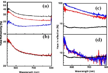
Figure 2.2 (a)Integrated (total) reflectivity of initial GaAs (100) flat substrate for TE and TM polarization
(black traces). Ssputtered GaAs substrates (ion fluence F2 = 4.9 1018 ions/cm2): red traces incident light polarized TE. Blue traces incident light polarized TM. (b) sample sputtered at fluence F3 = 3.49 1019 ions/cm2. All spectra have been normalized to the integrated reflectance standard RS2-Avantes (Al+MgF coating). (c)-(d) Haze in reflection: (black line) flat GaAs substrate, (red straight line) TE polarization (blue
line) TM for sample obtained at ion fluence: (c) F2 , (d) F3 .
In Fig. 2.2 (a) we plot the integrated reflectance spectra of the GaAs sample obtained by sputtering up to fluence F2 . Compared to a flat GaAs substrate (black trace, for which no distinctions between TE and TM polarizations are recorded), the TE spectra (red trace) shows a uniform decrease (about 10%) over the whole spectral range. The reduction of the reflected intensity is much more evident in the TM polarization (blue trace) and is more pronounced at short wavelengths: the total reflectivity shifts down from 40% to 20% at = 400 nm and from 30% to 20% at =800 nm. It is clear that the presence of sub-wavelength anisotropic surface corrugations is responsible of the occurrence of an anti-reflective behaviour with a strong dependence on incident polarization (dichroism). Reflection losses at the interface are thus reduced by the suppression of the Fresnel coefficients due to the progressive variation of the refractive index from air to substrate.
For the over-exposed sample the optical spectra are reported in Fig 2.2 (b); in this case no reduction of reflected intensity is recorded. The TE and TM integrated reflectance spectra overlap that of the flat substrate. The morphology of this sample shows that overexposing the substrate to the ion beam results in a significant coarsening of the smaller spatial components and only corrugations of low amplitude and with a lateral size remarkably larger than light wavelength are able to survive. This is clearly the motivation of the observed optical behavior, similar to the untreated flat GaAs surface.
GaAs: Haze measurements
In order to highlight the scattering properties of the textured substrates, we are interested in determining the diffuse scattering efficiency of the surfaces; therefore haze functions defined as the ratio of diffused and total reflected light, could be successfully used[28]. Measurements of the diffused light spectra have been performed by means of the integrating sphere and trapping the specular part of the reflected spectra. In Fig. 2.2 (c) we show the diffuse reflectance haze functions for sample obtained at fluence F2, it shows that off-specular light scattering is strictly dependent on the incident polarization and in particular it is more effective for light polarized perpendicular to the corrugation axis (TM polarization). Since light scattering is mostly related to the large scale surface features, i.e. larger than the wavelength of the incident light, normalized diffuse reflectance is strongly enhanced (above 50%) with respect to the flat case for both polarizations, at wavelengths shorter than 600nm. In the long wavelength region normalized diffuse reflectance rapidly decreases towards the value of the flat case remaining however higher than 20%. For the flat GaAs substrate (black trace), haze function remains throughout the considered wavelength range well below 10%; the non zero value is mainly related to the collection of a part of the specular reflected beam due to the dimension of the illuminating light spot. As expected, for the sample overexposed to high ion fluencies, light scattering is not very different with respect to a flat substrate, considering also the difference in the response to TE and TM polarized light throughout the considered wavelength range, Fig. 2.2 (d).
Experiments on Si
In order to generalize the results obtained for GaAs, we decided to perform the same experiments using a Si substrate which is another reference material for opto-electronic and photovoltaic devices. Employing the self-organized Au stencil mask and an ion fluence F2 (equivalent to the GaAs case) a nanoscale pattern was defined on the Si surface as shown in Fig. 2.3 (a). In order to quantitatively analyze the AFM morphology, in Fig 2.3 (b) we plot the corresponding height-height correlation function. The RMS roughness of the surface corrugations amounts to 40 nm and confirms that also in this case at the early stage of the process the pattern is transferred to the substrate with a vertical dynamic which is amplified with respect to the metal film. Comparing to the GaAs case at the same ion fluence, for silicon we observe an increase of the lateral correlation length that reads about 150 nm and a decrease of the mean slope of the surface features to 25°.
In this case, the optical spectra were measured employing an unpolarized light beam; the occurrence of an anti-reflective behavior in the VIS-NIR spectral range is made clear by comparing the total integrated
reflectance of the sample (blue trace reported in Fig 2.3 (c)) to that of a flat Si substrate (solid black line):
Figure 2.3: (a) AFM topography image of the Si surface sputtered at =82° and fluence= F2 = 4.9 1018
ions/cm2. (b) Log-log plot of the height-height correlation function from the height profile of the topography image. (c) Integrated (total) reflectivity for: flat Si substrate (upper solid black line), patterned
Si at =82° and fluence F2 (blue straight trace).(d) Haze function in reflection (ratio between diffused and total reflected light) for flat Si substrate (red line) and patterned Si (black trace).
the reflection losses are reduced by about 20% over the whole spectral range. The normalized diffuse reflectance data shown in Fig. 2.3 (d) (black line) confirm that at short wavelengths light is more effectively scattered at off-specular angles, while at large wavelengths haze is still 20% higher than the flat case (red trace) which, as discussed for the GaAs case, stays below 10% throughout the considered wavelength range.
Morphological and optical analysis allow us to draw some conclusions on the generality of the pattern transfer process between two different substrates, other conditions being equal, since the formation of the self-organised Au mask is equivalent on the two substrates. With respect to the value of the lateral correlation length for the ripple structures obtained on the gold mask at disconnection (fluence F2) an increase is observed both for the GaAs and for the Si substrates. This indicates that, due to enhanced mass transport mechanism (either thermally activated or ion induced), surface relaxation of the smaller features takes place efficiently while the decay of the larger structures requires a much higher irradiation dose as demonstrated by the overexposed GaAs sample. Despite the same sputtering conditions (incidence angle and fluence) employed, a 25% increase of the lateral correlation length and a 10% decrease of the rms roughness are in fact observed in the AFM investigations of Si substrata with respect to GaAs, indicating that the relaxation mechanism are more effective for Si in comparison to GaAs. The morphological differences of the two patterns are strictly related to the optical response summarized in Fig.5. Total integrated reflectivity under un-polarized illumination for the two samples is reported in Fig. 5 a) normalized to that of a flat substrate. In the GaAs case (black trace in the bottom) anti-reflection behaviour is more pronounced with respect to Si (red trace): the former substrate shows a 30% reduction of reflectivity across the whole wavelength range in comparison to the flat surface, while for Si the reflectivity only drops by 20%. In order to be suitable for technological application a more effective anti reflection behaviour is preferable and this can be obtained with arrays of very high aspect ratio (sharp) surface features exploiting the moth-eye effect on a wavelength range that can be tailored changing height, distance and width of the nanostructures [
14]. Arrays of GaAs and Si nanocones with base width in the range of 250 nm and height of 350 nm have shown a suppression of the reflectivity from the >30% of the bare wafer to well below 10% in the VIS-NIR range [29][30]. In our process the evolution of the features height occurs during the pattern transfer stage from the metallic mask and different strategies are now under scrutiny to prolong the life of the patterned
gold film. This is of primary importance to obtain a vertical dynamic further amplified, but at the same time a control of the lateral size enhancement is necessary in order to realize nanostructures with higher aspect ratio, especially in the Si case. The observed anti reflection behaviour turns out to be influenced by the pattern anisotropy as revealed by the integrated reflectance measurements with polarized light. We believe that a wide number of potential applications can take advantage of this property, as for example the realization of new optical elements in which a selectivity of the polarization response is required.
Discussion
The comparison of the morphological and optical analysis performed on Si and GaAs substrates allow us to draw some conclusions on the generality of the pattern transfer process between two different substrates, since the formation of the self-organised Au mask is equivalent on the two substrates. The experiments in particular reveal the importance of the diffusive relaxation processes in determining the final morphology of the pattern propagated through the stencil mask: substrates for which diffusive relaxation is effective tend in fact to coarsen efficiently the small scale sub-wavelength structures which are responsible for the moth-eye antireflection functionality. At the same time, the experiments indicate that the self-organised surface texturing based on IBS-IPL is promising in view of technological applications, especially for the synthesis of substrates with high haze in view of light trapping applications. The difference in the measure Haze between the two substrates studied is well correlated with the discrepancies observed in the morphological parameters of the substrates since, at fixed light wavelength, the haze function monotonically increases with the rms roughness of the surface and decreases with the lateral correlation length [31].
2.3 Transparent metal nanoelectrodes with plasmonic functionality
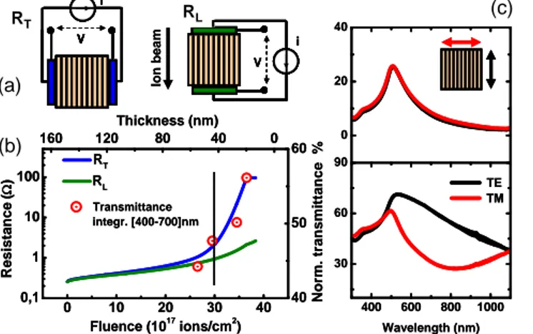
Here we also mention the recent developments of the activity initiate during the period 2010-11, aiming at the synthesis of semitransparent metal nanoelectrodes. The metal nanoelectrodes are intended to be optimised as an alternative to the conventional transparent conductive oxides, with the additional advantage of the plasmonic functionality. This activity led to the submission of two papers at primary international journals and a european patent has been officially registered [32]. The self-organised ion beam sputtering process has been optimised in order to transform the polycrystalline film into an array of nanowires with optimised sheet resistanace and optical transparency. In Figure 3.1(b) we show a representative plot of the sheet resistance measured along the nanowire axis (green trace) as a function of increasing ion fluence [33]. The end point of the experiment corresponds to a longitudinal sheet resistance
Ion bea m Rl i V Rl i V Rt i V Rt i V i V 0 10 20 30 40 0,1 1 10 100 RT RL R esistan ce ( ) Fluence (1017 ions/cm2 ) 160 120 80 40 0 40 50 60 Transmittance integr. [400-700]nm Thickness (nm) N o rm. tr an smittan ce % 400 600 800 1000 30 60 90 Wavelength (nm) 0 20 40 TE TM (a) (b) (c) RT RL Ion bea m Rl i V Rl i V Rt i V Rt i V i V 0 10 20 30 40 0,1 1 10 100 RT RL R esistan ce ( ) Fluence (1017 ions/cm2 ) 160 120 80 40 0 40 50 60 Transmittance integr. [400-700]nm Thickness (nm) N o rm. tr an smittan ce % 400 600 800 1000 30 60 90 Wavelength (nm) 0 20 40 TE TM (a) (b) (c) RT RL Ion bea m Rl i V Rl i V Rt i V Rt i V i V 0 10 20 30 40 0,1 1 10 100 RT RL R esistan ce ( ) Fluence (1017 ions/cm2 ) 160 120 80 40 0 40 50 60 Transmittance integr. [400-700]nm Thickness (nm) N o rm. tr an smittan ce % 400 600 800 1000 30 60 90 Wavelength (nm) 0 20 40 TE TM (a) (b) (c) RT RL
Figure 3.1: (a) Sketch of the 4-wires measurements scheme employed to determine the sheet resistance of
the NW arrays. (b) Real-time evolution of the sheet resistances measured during sputtering, respectively along parallel (green trace) and orthogonal (blue trace) directions with respect to the ripples. (c) Transmission optical spectra of a sputtered Au electrodes supported on glass substrate before the film disconnection (upper panel) and at the end of the sputtering (bottom panel) when the ripple pattern has
decomposed into ordered NWs.
of about 2 Ohm/sq. We must recall that these values are competitive with those of the best TCOs based on ITO which exhibit typical sheet resistances in the 20 Ohm/sq range. One must also stress that the nanowire electrodes allow to transform an isotropic film into a strongly anisotropic conductor since the transverse sheet resistance reads about 100 Ohm/sq.
The experiments also allowed to tailor the optical transparency of the metal electrode, (red circles) in figure 3.1(b), by increasing ion fluence. For an Au film with initial thickness of 150 nm, the IBS nanopatterning leads to the formation with an integrated transmittance of about 57% in the VIS-IR range. It is possible to optimise the optical transmittance of the semitransparent nanoelectrodes by modifying the initial thickness of the polycrystalline film prior to IBS ion irradiation. In this way, for films with initial thickness around 80-100 nm the optical transmittance increases to about 75% [34].
In Figure 3.2(c), optical extinction spectra of polarized light are plotted for a connected continuous film (top panel) and for an array of Au nanowires (bottom panel) are shown. The spectra evidence that, when the film decomposes into an array of disconnected nanowires, transversely polarised light (TM polarization) is able to excite localised Plasmon resonances across a broad range of wavelengths across the VIS–NIR region of the light spectrum. This feature renders the nanowire arrays interesting in view of photon harvesting applications induced by plasmonic scattering [7,33] and in also in view of non-linear and bio-sensing applications [35,36]
Conclusions
In this activity we have explored the possibility nano-textured surfaces on technologically relevant materials by low energy ion beam sputtering (IBS) employing a pattern transfer process from a self-organized metallic mask. The aim is to highlight the potentiality of the so-patterned substrates in view of technological applications in the photovoltaic field. We have investigated the morphological evolution of the surfaces of Glass, TCO (AZO), GaAs and Si substrates as a function of ion fluence by means of AFM measurements and we have characterized their optical properties in terms of total and diffuse reflectivity. At low ion fluence, optical measurements on samples have demonstrated the occurrence of a polarization dependent anti-reflection behaviour in the VIS-NIR range induced by the presence of sub-wavelength surface features; light scattering at off-specular angles due to the larger scale modulations is confirmed by the high values of the haze functions in reflection .
In the case of Glass and AZO substrates, the substrates have been employed as supports for a:Si thin film PV devices grown by ENEA. The solar cells show an overall improvement of the spectral response with respect to the reference device grown on unstructured glass substrates. Enhancement of external quantum efficiency (EQE) in the 400-800 nm wavelength range is observed with a short circuit current densities (J sc ) improvement up to 15 %.
The experiment performed in Genova have also demonstrated that the self-organised IBS process can be adapted to form arrays of semitransparent nano-electrodes beginning from a flat polycrystalline Au film. Beyond from the extremely low sheet resistances, which render the metal nanowire arrays competitive with the best conventional TCOs, the nanoelectrodes support localised Plasmon resonances which make them appealing in view of photon harvesting applications in photonic devices and in biosensors.
References
(in bold works with ENEA-MSE acknowledgment)[1] Green, M. A. Solar Cells: Operating Principles, Technology and System Applications (Univ. New South Wales, 1998).
[2] Yablonovitch, E. & Cody, G. D. Intensity enhancement in textured optical sheets for solar cells. IEEE Trans. Electr. Dev. 29, 300-305 (1982).
[3] Deckman, H. W., Roxlo, C. B. & Yablonovitch, E. Maximum statistical increase of optical absorption in textured semiconductor films. Opt. Lett. 8, 491-493 (1983).
[4] A.Naqavi et al. “Understanding of photocurrent enhancement in real thin film solar cells: towards optimal one-dimensional gratings” Optics Express 19, 128 (2010).
[5] C.Battaglia et al. “Nanomoulding of transparent zinc oxide electrodes for efficient light trapping in solar cells ” Nature 5, 535 (2011)
[6] P. Vukusic and J.R.Sambles “Photonic structures in biology” Nature 424, 852 (2003) [7] H.A. Atwater and A. Polman Nature Materials 9, 205 (2010)
[8] E.Fortunato MRS Bulletin 32, 242-247 (2007) [9] S.A. Maier et al., Nature Materials 2, 229 (2003) [10] N.A. Melosh et al. Science, 300, 112 (2003). [11] Yao Lin et al. Nature 434, 55-59 (2005).
[12] W.A. Lopes and H.M. Jaeger Nature 414, 735-738 (2001). [13] C.J.Murphy et al. MRS Bull. 30, 349 (2005).
[14] Boden, S.A. and Bagnall, D.M. (2008) “Tunable reflection minima of nanostructured antireflective surfaces.” Appl. Phys. Lett. 93, 133108-133110
[15] D. Chiappe, A. Toma, Z. Zhang, C. Boragno, F. Buatier de Mongeot, “Amplified Nanopatterning by Self-Organised Shadow Mask Ion Lithography” Applied Physics Letters , 97, 053102 (2010)
[16] Z. Q. Zhang, D. Chiappe, A. Toma, C. Boragno, J. D. Guo, E. G. Wang, F. Buatier de Mongeot , “GaAs nanostructuring by self-organized stencil mask ion lithography” Journal of Applied Physics, 110, 114321 (2011)
[17] C.Martella, D.Chiappe, F. Buatier de Mongeot, P. Delli Veneri, L.V.Mercaldo, I.Usatii, “Self-organised broadband light trapping in thin film a:Si solar cells” Nanotechnology, under submission (2012)
[18] C.Martella, M.Giordano, C. Mennucci, F. Buatier de Mongeot, P. Delli Veneri, L.V.Mercaldo, I.Usatii, “Broad-band Photon Harvesting in Nanostructured a:Si Thin Film Solar Cells” Proceedings 27th European
Photovoltaic Solar Energy Conference, Frankfurt, Germany (2012).
[19] Haug F J, Söderström K, Naqavi A and Ballif C 2011 J. Appl. Phys. 109 084516
[20] C.Martella, D.Chiappe, A.Toma, F. Buatier de Mongeot, “Enhanced broadband light scattering from
Self-organised Si an GaAs gratings” in preparation (2012)
[21] S.W.MacLaren, J.E.Baker, N.L.Finnegan, and C.M.Loxton, J. Vac. Sci. Technol. A 10, 468 (1992).
[22] D. Datta, S.R. Bhattacharyya, T.K. Chini, and M.K. Sanyal, Nucl. Instrum. Methods Phys. Res. B 193, 596 (2002).
[23] Y. Wang, S.F. Yoon, C.Y. Ngo, C.Z. Tong, and C.Y. Liu, J. Appl. Phys. 106, 24301 (2009).
[24] A. Toma, D. Chiappe, B. Šetina Batič, M. Godec, M. Jenko, F. Buatier de Mongeot Physical Review B 78, 153406 (2008).
[25] I. Horcas, R. Fernandez, J. M. Gomez-Rodriguez, J. Colchero, J. Gomez-Herrero, and A. M. Baro, Rev. Sci. Instrum. 78, 013705 (2007).
[26] Y.-P. Zhao, G. –C. Wang, and T. –M. Lu, Phys. Rev. B 58 (11), 7300 (1998). [27] H. –N. Yang, and T. -M Lu, Phys. Rev. B 51 (4), 2479 (1995).
[28] K. Jäger, M. Fischer, R.A.C.M.M. van Swaaij, and M. Zeman, J. Appl. Phys. 111, 083108 (2012). [29]C.-H. Sun, B. J. Ho, B. Jiang, and P. Jiang, Opt. Lett. 33 (19), 2224 (2008).
[30]J. Zhou, M. Hildebrandt, and M. Lu, J. Appl. Phys. 109, 053513 (2011).
[31] I. Simonsen, Ǻ. Larsen, E. Andreassen, E. Ommundsen, and K. Nord-Varhaug, Phys. Rev. A 79, 063813 (2009).
[32] European Patent n. EP2274779 (04.01.2012) “Method for the synthesis of an array of metal nanowires supporting localized Plasmon resonances , and photonic device comprising said array”F.Buatier de Mongeot, C.Boragno, U.Valbusa, D.Chiappe, A.Toma.
[33] Daniele Chiappe, Andrea Toma, and Francesco Buatier de Mongeot
“Tailoring resisitivity anisotropy of nanorippled metal films: Electrons surfing on gold waves”Phys. Rev. B 86, 045414 (2012)
[34] Daniele Chiappe, Andrea Toma, and Francesco Buatier de Mongeot
“Transparent plasmonic nanowire electrodes via self-organised ion beam nanopatterning” Small, under review (2012)
[35] A. Belardini, M. C. Larciprete, M. Centini, E. Fazio and C. Sibilia, D. Chiappe, C.Martella, A. Toma, M. Giordano, F. Buatier de Mongeot “Circular Dichroism in the Optical Second-Harmonic Emission of Curved Gold Metal Nanowires” Phys Rev. Lett. 107, 257401 (2011)
[36] A. Belardini, F.Pannone, G. Leahu, M. C. Larciprete, M. Centini, C. Sibilia, C.Martella, M. Giordano, D.Chiappe and F. Buatier de Mongeot “Evidence of anomalous refraction of self-assembled curved gold nanowires” Appl. Phys. Lett. 100, 251109 (2012);
Description of the Host Laboratory and CV of the principal Investigator.
The Laboratory of Nanostructures is active at the Department of Physics of the University of Genova, Italy. The research activity mainly deals with the development of self-organised nano-patterning processes of surfaces and films, in particular recurring to defocused Ion Beam Sputtering. Beyond promoting morphological and structural modification of extended sample areas in a single maskless step, the nanopatterning process allows to tailor important functional properties which range e.g. from photonics, to nanomagnetism, tribology, catalysis, plasmonics and electrical transport.Principal Investigator, prof. Francesco Buatier de Mongeot, was born in Genova (Italy) July 11th,1965. He is Associate Professor in Condensed Matter Physics at the Physics Department of the University of Genova since 2010.
Here follows a brief CV of the principal investigator #Studies:
1991 Master in Physical Sciences (Laurea in Fisica) University of Genova, Italy 1994 Ph.D. in Physics at the University of Genova
#Post-Doctoral Activity:
1994-1995 Grantee of the Italian National Research Council (CNR).
1995-1997 Visiting Researcher (Alexander von Humboldt fellowship) at the Department of Surface Chemistry and Catalysis, University of Ulm (Germany)
1997-1998 Post doctoral fellow of the University of Genova 1998-2000 Reserarcher at INFM - Unit of Genova
2000-2009 Staff Researcher in Condensed Matter Physics at the Physics Department of the University of Genova
2005- Guest professor at the Institute of Experimental Physics, Jagiellonian University, Krakow, Poland
-Fellow of the Alexander Von Humboldt Stiftung
-Winner of a selection of Functionner of the EU Commission-Directorate of Research (COM/A/3/02). Member of the Reserve list od European functionners.
#Teaching activity:
-professor in charge the following undergraduate and graduate courses: Solid State Physics, Structure of Matter, General Physics, Nanostructures, Introduction to Solar Cells, Laboratory of Experimental Physics. -Supervision of Theses: He has been the supervisor of more than 20 Master or Bachelor Thesis projects, of 6 PhD students, of 5 post-docs.
#Summary of research activity:
#Scientific management:
- (2001-2004): Scientific Manager (INFM research unit in Genova) of a National project PRA-NanoRub (National research collaboration on Nanofriction)
- (2002-2005): Scientific Manager (INFM research unit of Genova) within a FIRB national project dealing with self- and nano-scale organisation of molecules for magnetic and optical applications.
-(2006) : National coordinator and scientific manager of a high relevance bilateral project Italy-Slovenia financed by the Ministry of Foreign Affairs “Nanofabrication of functional materials by ion beams “
-(2006-2008) : National coordinator of a research program financed by the National Consortium of Condensed Matter Research (CNISM). “Metal nanowires for bio&nano photonics”.
-(2006-2009) : National coordinator and Scientific manager for of a high relevance bilateral project Italy-China financed by the Ministry of Foreign Affairs “Guided self-organisation of Nanostructures” (budget for mobility).
-(2007) : National coordinator and scientific manager of a high relevance Italy-Slovenia bilateral project financed by the Ministry of Foreign Affairs “Nanofabrication of functional materials by ion beams “
-(2008) : National coordinator and Scientific manager for of a high relevance Italy-Poland bilateral project financed by the Ministry of Foreign Affairs “Self-organised synthesis of supported metal nanostructures”. -(2009-2010) : Coordinator of a project in collaboration with ENEA on “Plasmon enhanced Photon Harvesting for Photovoltaic Applications”. Funded by ENEA-Ministero Sviluppo Economico
-(2009) : National coordinator and Scientific manager for of a high relevance Italy-Poland bilateral project financed by the Ministry of Foreign Affairs “Self-organised synthesis of supported metal nanostructures”. -(2010) : National coordinator and Scientific manager for of a high relevance Italy-Poland bilateral project financed by the Ministry of Foreign Affairs “Self-organised synthesis of supported metal nanostructures”. -(2010-2013): Competitive Grant funded by Liguria Region (European Funds P.O. C.R.O. FSE 2007-2013). Progetto “Materiali Funzionali Nanostrutturati per applicazioni Fotovoltaiche Avanzate”
-(2010-2011) : Local coordinator and scientific manager of PRIN national project financed by the Ministry of University “Plasmonics in metallic self-organized nanoparticles “
-(2010-2011): Coordinator of a research project financed by the CARIGE Foundation “Materiali Funzionali Nanostrutturati per applicazioni Fotovoltaiche Avanzate”
-(2010-2011) : Coordinator of a project in collaboration with ENEA on “Plasmon enhanced Photon Harvesting for Photovoltaic Applications”. Funded by ENEA-Ministero Sviluppo Economico.
-(2011-2012) : Coordinator of a project in collaboration with ENEA on “Photon harvesting from nanostructured metallo-dielectric substrates”. Funded by ENEA-Ministero Sviluppo Economico
-(2012) : Marie Curie Initial Training Networks (ITN) “Novel Transparent Conductor Concepts for photovoltaic applications” Submitted
-(2012-2014): Competitive Grant funded by Liguria Region (European Funds P.O. C.R.O. FSE 2007-2013). Progetto “Substrati Nanostrutturati Funzionalizzati per applicazioni fotovoltaiche e fotoniche”
-(2012-2014): Competitive Grant funded by Liguria Region (European Funds P.O. C.R.O. FSE 2007-2013). Progetto “Crescita e caratterizzazione dei difetti in Film micro- e nano-strutturati”
- He is Referee for the international Journals Nature Nanotechnology, Physical Review Letters, Physical Review B, Physical Review E, Applied Physics Letters, Applied Surface Science, Applied Physics A, Nanoscale, Semiconductor Science and Technology, Thin Solid Films, Materials Letters.
- Evaluator and Project Reviewer: National Scientific Research Council of Romania, US Dept. of Energy (DOE), Foundation for the Fundamental Research on Matter (FOM) Netherlands, National Research Foundation (NRF) of South Africa.
-He is author of almost 100 scientific pubblications on international refereed journals, among which Nature Materials, Physical Review Letters, Advanced Materials, Small, ACS Nano, JACS, Optics Express.
-Invited speaker at more than 35 international conferences and seminars, among which American Physical Society March meeting Montreal,2004), American Association of Crystal Growth (Lake Tahoe,USA 2005, European Conference On Surface Science ECOSS (Berlin, 2005), MRS fall meeting (Boston, 2006), SPIE meeting "Microelectronics, MEMS, and Nanotechnology" , Canberra, Australia (2007).