i
UNIVERSITÀ DEGLI STUDI DI CATANIA
FACOLTÀ DI SCIENZE MATEMATICHE FISICHE E NATURALIDottorato di Ricerca in Scienza dei Materiali (Ph.D in Materials Science)
XXIV ciclo
Chemical Engineering of Silicon for
Supramolecular Recognition
D
OTT
.
SSA
C
RISTINA
T
UDISCO
Tutor:Chiar.mo Prof. G.G. Condorelli
Coordinatore: Chiar.mo Prof. A. Licciardello
ii
Contents
Aim of the work………...1
Chapter 1………..3
1.1 Introduction……… 3
1.1.1 Nanotechnology and nanomaterials……… 3
1.1.2 Self Assembled Monolayer………... 5
1.1.3 Basics of SAMs………7
1.1.4 Chraracterization of SAMs………...8
1.1.5 SAMs on silicon surface………...9
1.1.5.1 Flat, single crystal silicon………... 11
1.1.5.2 Porous Silicon………..11
1.1.5.3 SAMs on native silicon oxide………..12
1.1.5.4 SAMs directly on bare Si……….13
1.2 Chemical Sensors………. 25
1.3 Cavitands……….. 30
1.3.1 Quinoxaline-salen-bridged cavitands………...31
1.3.2 Phosphorous bridged cavitands………33
1.4 References……… 37
Chapter 2 Flat Silicon grafting of Tetraphosphonate cavitand for molecular recognition: from sensing to nanoengineering of functional molecules ………..44
2.1 Introduction……….. 44
2.1.1 Molecular recognition of N-methylated amino acids: sarcosine detection as tumoral marker………..45
2.1.2 Hierarchical Self-Assembly of luminescent system……… 47
iii
2.2.1 Synthesis of Tiiii, TSiiii, ammonium salts and lanthanide
complexes………. 48
2.2.2 Synthesis of Tiiii……….. 49
2.2.3 Preparation of Tiiii-grafted Si surface (Si-Tiiii)……….. 50
2.2.4 Monolayer Characterization……… 50
2.3 Molecular Recognition of sarcosine in urine………... 51
2.3.1 Sarcosine complexation in the solid state………... 51
2.3.2 Sarcosine complexation in solution……… 54
2.3.3 Sarcosine complexation at the solid-water interface…………... 56
2.3.4 Sarcosine detection in urine………. 59
2.3.5 Conclusions……….. 62
2.4 Hierarchical Assembly of lanthanide complex through molecular recognition……….. 63 2.4.1 XPS Characterization………... 64 2.4.2 Fluorescence Characterization………. 70 2.4.3 Conclusions……….. 74 2.5 References……… 75 Chapter 3 Functionalization of porous silicon with cavitand-based receptors………. 80
3.1 Introduction………...……...80
3.2 General Procedures………...…82
3.2.1 Synthesis of 1………... 82
3.2.2 Synthesis of methyl esters of AcIN, AcOUT cavitands, and MeCav cavitand………....83
3.2.3 Porous Silicon preparation……….……. 83
iv
3.2.5 Monolayer Characterization……….84
3.2.6 Computational details………..85
3.3 Covalent Functionalization of Silicon Surfaces with a Cavitand-Modified Salen………...86
3.3.1 XPS Characterization………... 87
3.3.2 FTIR Characterization of PSi-1………... 91
3.3.3 AFM Lithography on Si-1………94
3.3.4 Surface synthesis of uranyl complexes……… 95
3.3.5 Conclusions………..97
3.4 Detection of DMMP by cavitand functionalized PSi………... 98
3.4.1 Sensing of organophosphorus vapors………...98
3.4.2 Chracterization of Cavitand functionalized PSi……….…100
3.4.3 DMMP complexation: XPS, FTIR and thermal desorption study………104
3.4.4 Organophosphours vapor complexation: theoretical modeling……….109 3.4.5 Conclusions………113 3.5 References………..………115 Chapter 4 Concluding Remark…………..……..………...124 Acknowledgments...126
1
AIM OF THE WORK
This thesis discusses some strategies to anchor functional molecules on silicon-based substrates in order to introduce onto a solid surface specific functionalities. Two main typologies of silicon-based substrates both of technological interest have been functionalized through synthetic routes based on the hydrosilylation reaction. First typology consists of flat monocrystalline Si(100) which is the surface of election for the development of commercial microelectronic devices, while second substrate typology consists of porous silicon which represents an interesting candidate for novel devices due to its specific properties such as high surface area and luminescence. In particular, the attention is focused on the surface grafting of cavitand-based molecules, synthetic organic compounds with rigid cavities of molecular dimensions, which are interesting and versatile receptors. A key point of this thesis has been the study of the recognition properties of these receptors after surface anchoring. The obtained hybrid materials consisting of cavitand monolayer bonded to silicon surface combined the technological advantages of either Si(100) or porous silicon substrates with the recognition properties of cavitand, thus allowing various applications ranging from sensing to surface hierarchical nanoassembly.
3
Chapter 1
1.1 Introduction
1.1.1 Nanotechnology and nanomaterials
In 1959, Nobel award winner Richard Feynman first proposed the seminal idea of nanotechnology by suggesting the development of molecular machines. Ever since, the scientific community has investigated the role that nanotechnology can play in every aspect of society. Nanotechnology refers to the research and technology development at atomic, molecular, and macromolecular scales, which leads to the controlled manipulation and study of structures and devices with length scales in the range of 1-100 nanometers. One nanometer (nm) is one billionth of a metre; tens of thousands of times smaller than the width of a human hair (figure 1.1.1).
4
Figure 1.1.1: Objects of approximate size from 1 m to 10-10 m.
In the last two decades, the research of nanotechnology has grown explosively with over three hundred thousands publications in the field of nanoscience according to Web of Science1.
The intrigue of nanotechnology comes from the ability to control material properties by assembling such materials at the nanoscale. The tunable material properties that nanotechnology can provide were stated in Norio Taniguchi’s paper in 1974 where the term ‘‘nanotechnology’’ was first used in a scientific publication. Recently, nanomaterials, which are materials with basic structural units, grains, particles, fibers or other constituent components smaller than 100 nm in at least one dimension, have evoked a great amount of attention for improving disease prevention, diagnosis, and treatment.2
5
Nanostructured materials with tunable morphology have attracted exceptional interest over the past decades because of their unique architectures, tailored physicochemical properties, central roles in fabricating nanoelectronics, and potential applications in bionanotechnology. In recent years, a vast array of novel nanostructures have been manufactured and studied in the interdisciplinary fields of nanoscience, material science, biological science, etc. Thus far, lots of investigations with respect to inorganic nanomaterials have been reported and well documented, as summarized by recent review articles3. Compared with inorganic nanostructures, the organic counterparts have, in particular, fascinated scientists because of their multifunctionality, considerable variety and flexibility in molecular design, and solution processability. These advantages make the organic nanostructures promising candidates for electronics, including organic field-effect transistors, organic light emitting displays, nanosensors, etc. Thus, the exploration of the controlled synthesis of organic nanostructures is a significant issue.4
1.1.2 Self Assembled Monolayer
The term “self-assembling monolayer” was coined in 1983 in New Scientist5 in an anonymous report describing the work of Lucy Netzer and Jacob Sagiv on the chemically controlled layer-by-layer self-assembly of multilayer films.6 The self assembly of adsorbates on an appropriate surface has been known since 1946, when Zisman and co-workers reported the formation of monomolecular films of long-chain hydrocarbons carrying polar groups on a variety of polar surfaces.7,8 Although these films are extremely thin (typically ca. 2 nm), they are able to completely change the surface properties.
However, the versatility of these adsorbed monolayers was not realized until 1978, when Polymeropoulos and Sagiv proposed their use for measuring electrical conduction between two metal surfaces.9 In 1980, Sagiv published the first article
6
demonstrating the formation of well-defined organosilane monolayers on SiO2 by
direct adsorption (that is, self-assembly) from solution.10,11
Nowadays it is well know that Self-assembled monolayers (SAMs) provide a convenient, flexible, and simple system with which to tailor the interfacial properties of metals, metal oxides, and semiconductors. SAMs are organic assemblies formed by the adsorption of molecular constituents from solution or from gas phase onto the surface of solids or in regular arrays on the surface of liquids (in the case of mercury and probably other liquid metals and alloys); the adsorbates organize spontaneously (and sometimes epitaxially) into crystalline (or semicrystalline) structures.12
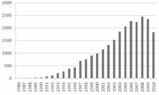
The method of self-assembled monolayers (SAMs) has witnessed exponential growth in synthetic sophistication and depth of characterisation over the last two decades. Figure 1.1.2 presents graphically the increasing number of articles/reports published per year in the fields of SAMs in the last two decades
7
The success of SAMs is due likely to their ability to create controlled surface chemistry with high molecular organization and defined stoichiometry over relatively large areas. SAMs have facilitated the study of molecular and cellular interactions with specific functional groups, surface energetic, surface charge, or other interface properties. SAMs can be used to include specific functionalities or ligands to study biological interactions such as cell signalling, cell adhesion,13 and
protein interactions.14,15 SAMs have also been used for constructing molecular switches,16 biosensors17 and microarrays. SAMs offer a unique combination of physical properties that allow fundamental studies of interfacial chemistry, solvent-molecule interactions and self-organization.
1.1.3 Basics of SAMs
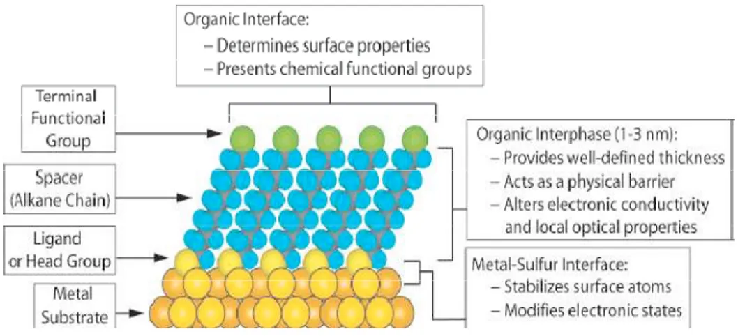
A schematic of an organic SAM is shown in Figure 1.1.3. Usually, SAMs are formed spontaneously by immersing Si substrates into an active solution, e.g. surfactant molecules R(CH2)nSiX3 (X = Cl, OCH3 or OC2H5) dissolved in
alkane/carbon tetrachloride.
However, the SAMs can be deposited by other techniques as well, such as, vapor deposition. The self-assembling monolayer can be divided into three parts:
8
Figure 1.1.3: A schematic diagram showing different parts of a self-assembled monolayer on a metal surface.
(i) Head group, i.e. SiX3. It forms the chemical bond with surface atoms of the
substrate (exothermic: ~40-45 kcal/mol or ~1.7 eV) causing the pinning of surfactant molecule to the substrate.
(ii) Alkyl chain, i.e. (CH2)n. The inter-chain van der Waals interactions (exothermic
<10 kcal/mol or <0.4 eV) could assist in formation of an ordered molecular structure. Of course, the possibility of obtaining ordered structures depends on the pinning density of the head groups.
(iii) Surface group, i.e. R. This is the terminal group which is replaced with or bonded to different functional groups to obtain specific applicative devices.
1.1.4 Characterization of SAMs
The quality of deposited SAMs is assessed by characterizing them for (i) thickness, (ii) molecular orientation and ordering, (iii) uniformity and coverage, (iv) chemical composition, and (v) thermal and chemical stability.
9
Various techniques are available for the characterization of monolayers18. The chemical composition of monolayers can be determined by Auger electron spectroscopy (AES), X-ray photoelectron spectroscopy (XPS) and secondary ion mass spectroscopy (SIMS). Only XPS can reliably characterize the chemical composition of organic ultrathin layers on metallic substrates With this method, which is possible only under UHV conditions, photoelectrons are released from the substrate by incoming X-rays and subsequently analyzed with respect to their kinetic energy. In this analysis, the core level binding energies of electrons can be determined, in turn allowing inferences about the chemical composition (elemental distribution and chemical state of the elements) of the examined sample.
1.1.5 SAMs on silicon surface
Although SAMs on gold have received more attention than the other typologies of SAMs, presumably because of their ease of preparation, monolayers on silicon surface possess some advantageous features. The covalent nature of the assembly process results in systems possessing superior stability, which allows extensive handling and further modification steps without deterioration of the monolayer.11 Silicon is the cornerstone of the microelectronics industry. In spite of uncertainties concerning looming limitations of feature sizes on chips within a decade, silicon will most likely remain a central material in computing technologies. The incredible degree of structural control over silicon, based on engineering and chemistry developed over the years by industry and academia, makes it practical to keep silicon as the platform on which complex molecular devices will be built. Research efforts to build hybrid silicon-organic structures are growing rapidly in both academia and industrial companies.19 This approach to meeting future microelectronics demands by merging molecules with silicon is also critical for various applications that use silicon, but not necessarily for computing. For
10
instance, the integration of sensors with silicon, in-vivo drug delivery devices, microfluidics and labs-on-chips, bioanalysis, new catalytic materials, and many others, all based on silicon, are areas of intense interest. While the overall technological goals may be very different, all are related by the fact that surface properties of the silicon need to be tailored and controlled. For sensing, for instance, specificity must be introduced by attachment of recognition elements. For molecular electronics, on the other hand, molecules with specific electronic properties must be bound to the silicon surface in a way that is fluid or open to electrons and electronic information. Similar points can be made for most silicon-based applications for which the surface properties are critical.
While native oxide on silicon has proven extremely useful in the electric passivation of bulk silicon, much attention is being directed towards the synthesis of organic monolayers which can be modified upon demand for specific requirements. A wide variety of functionalities can be synthesized and incorporated which will allow for fine tailoring of surface characteristics for a broad range of applications. For the functionalization of silicon surface several different approaches have been taken to first understand its reactivity, and then to subsequently exploit the reactivity to prepare stable, sophisticated interfaces. In addition to chemical properties of silicon surfaces, surface morphology must also be considered. A morphologically complex (i.e. rough) surface will have different characteristics from a flat surface. A surface that is not flat will have greater surface area that could be highly advantageous for sensing and analysis, for instance, since a much larger quantity of the recognition agent could be packed onto the exposed surface.
A very interesting variant of flat, single crystalline silicon is porous silicon.20 This high surface area wafer formed from the same silicon wafers used in microelectronics has many advantages and attractions that result from its porosity21.
11
Porous silicon can have surface areas of 500 m2xcm-3 which is far greater than a sample of atomically flat silicon.
The approaches towards preparation of monolayers through Si-C bonds on both flat and photoluminescent porous silicon are described in the following paragraphs.
1.1.5.1 Flat, single crystal silicon
Single crystal silicon wafers of high purity are commercially available and relatively inexpensive due to their wide use in microelectronic applications. The most common surface orientations are Si(111) and Si(100) although other Si(hkl) orientations are known. Upon exposure to air, single crystal silicon becomes rapidly coated with a thin, native oxide that can be removed chemically with fluoride ion or thermally under UHV conditions. Depending upon the desired electronic properties, silicon wafers are doped in a controlled fashion with electron donating (P, As, Sb: n-type) or withdrawing (B: p- type) impurities to render the intrinsic material more highly conducting.
1.1.5.2 Porous Silicon
Porous silicon is a potentially revolutionary variant of crystalline silicon because of its tunable electro-, photo- and chemo-luminescent properties.22 While bulk silicon is an extremely poor light emitter, porous silicon can achieve quantum efficiencies in excess of 10%, the earliest initial application envisaged for the material was optoelectronics, the integration of optical transduction with the electronics of silicon, but then was soon accompanied by sensing, bioanalysis and nanocrystalline silicon fundamentals, using the high surface area.
Because it is easily prepared through simple galvanostatic,23 chemical (stain),24 or photochemical25 etches from silicon wafers (‘bucket’ chemistry),22 porous silicon
12
could be readily integrated with silicon-based integrated circuit (IC) manufacturing processes.
The native surface of porous silicon, produced via electrochemical and chemical etches, is capped with hydrogen. In order to satisfy the tetravalency requirement of each silicon atom, the surface is capped with one, two or three hydrides. This surface is termed ‘metastable’ because this surface can be handled briefly in air for minutes or in some cases hours, but is reactive enough to use the Si-H groups as chemical handles through which further chemistry may be accomplished. Porous silicon has the added advantage of being transparent to infrared (IR) radiation, and combined with its high surface area, its surface terminations can be analysed directly by IR spectroscopy.
1.1.5.3 SAMs on native silicon oxide
The native oxide layer usually contains a high density of traps therefore, it is desirable to remove the native oxide layer and grow an ultra-thin (1-1.5 nm) thermal oxide layer of better electrical quality. On a silicon oxide surface, three classes of molecules, namely, silanes (RSiX3, with X= Cl, OMe, OEt),
organometallics (RLi or RMgX), and alcohols (ROH) are widely used for the formation of self assembled monolayers. Thorough cleaning of the substrate is a prerequisite for obtaining a clean oxide layer with high density of silanol groups (Si-OH) on the surface. These silanol groups, which provide a highly hydrophilic surface (allowing molecules to diffuse on the physisorbed ultra-thin water layer), are either used as anchoring sites for silanization reactions or converted into more reactive functions (i.e. Si-Cl or Si-NEt2) suitable for alkylation or alkoxylation
13
1.1.5.4 SAMs directly on bare Si
For certain investigations pertaining to molecular electronics applications, the presence of native oxide layer between organic molecule and Si might cause some hindrance, e.g. to study an interface between the organics and Si. Thus, in order to deposit organic SAMs directly on the Si following two steps are necessary, (i) complete removal of the native oxide layer and obtain a reactive surface precursor and (ii) formation of organic SAMs on the freshly prepared reactive surface precursor by making Si-C or Si-O bonds.
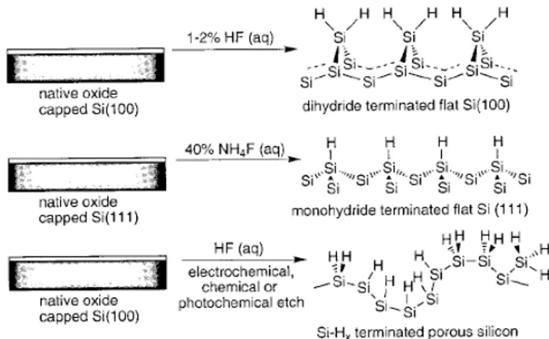
There are three known strategies to obtain a reactive Si surface precursor namely, (i) hydrogen-terminated Si, (ii) halogenterminated Si and (iii) reconstructed Si surface. First reactive surface, obtained with Si-H passivation, is only metastable with respect to oxidation under ambient conditions, thus precluding long-term use in most cases. These surfaces can, however, be handled in air for tens of minutes with little degradation which renders them accessible to chemists and materials scientists wishing to use standard Schlenk and glove box techniques.26 Silicon-hydride termination of commercial, native oxide capped flat crystal silicon wafers is carried out quickly and efficiently in less than10 min using commercially available fluoride sources. To obtain H-terminated flat silicon surfaces two etching process can be employed as shown in figure 1.1.4.
Dilute (1–2%) aqueous HF treatment of a Si(100) wafer yields the (100) dihydride =SiH2 capped surface, and 40% aqueous NH4F of a Si(111) wafer provides the atomically flat (111) monohydride ≡SiH terminated surface.27 Porous silicon, when etched through standard procedures involving HF, is also hydride terminated but it is coated with –SiH3, =SiH2, ≡SiH groups in a variety of different local orientations
and environments owing to the porous nature of the material. All the freshly etched silicon hydride terminated surfaces are chemically homogeneous ( > 99% H termination) which is essential for clean reactions. The hydride terminated surfaces
14
are extremely useful surface precursors because the Si–H and Si–Si bonds can serve as chemical handles through which functionalization can be mediated.
Figure 1.1.4: Fluoride-based etching conditions, leading to hydride-terminated flat and porous silicon surfaces.
Different methods employed to obtain halogen terminated Si surface are presented in figure 1.1.5.
15
The Chloro-terminated Si surfaces are prepared by treating the H-terminated Si (11 1) with PCl5 at 80-100 °C using benzoyl peroxide as a radical initiator in
chlorobenzene.28,29 The other methods include (i) boiling Si wafer in chlorobenzene
with PCl5 and UV irradiation, and (ii) heating H-terminated Si at 80 °C in the presence of chlorobenzene.30 Recently, high quality of halogenated silicon surfaces has been produced using gas phase reactions of hydrogenated silicon with molecular chlorine or bromine at room temperature.31 Bromo-terminated Si
surfaces can also be obtained by treating the H-terminated Si surface with CCl3Br
at 80 °C under UV irradiation. Bromination of Si−H surface is also performed sometime using an etching mixture made of HF, HNO3, CH3CO2H, Br2 and KBr,32
but this method causes morphology changes of silicon surface.33 Iodine34 or iodoforme35 have also been used as iodinating agents to generate Si−I surface from hydrogenated silicon. The halogen-terminated surfaces are very reactive and thus need to be handled only under inert atmosphere.
Highly reactive bare silicon (100) and (111) surfaces can be obtained by heating Si wafers at temperatures >700 °C under ultra high-vacuum (UHV) conditions (>10-10 Torr). Both the (100) and (111) Si surfaces undergo extensive reconstructions, i.e. their surface atomic geometry differs significantly from that of the bulk. However, the two surfaces have markedly different surface structures.
Treatment of a freshly etched hydride-terminated porous silicon surface with molecular chlorine, bromine, and iodine under nitrogen or argon results in efficient Si-X (X ) Cl, Br, I) bond formation in 30 min at room temperature. In contrast to the preceding reactions on flat Si(111) surfaces, the hydrides remain intact and are not substituted by chloride; the weaker Si-Si bonds are cleaved and two new Si-X bonds are formed.
The surfaces of silicon have several different chemical reactive sites through which functionalization may be obtained. The general mechanistic trends, based on
16
hydrosilylation, for flat and porous silicon interfaces are very closely related and thus are discussed here interchangeably.
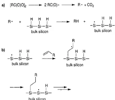
Hydrosilylation involves insertion of an unsaturated bond into a silicon–hydride group as shown in figure 1.1.6. Alkyne and alkene hydrosilylation on Si–H terminated surfaces yields alkenyl and alkyl termination, respectively. The first example of hydrosilylation of non-oxidized Si–H passivated silicon was carried out by Chidsey and coworkers in 1993 on flat crystal Si(111)
Figure 1.1.6: Hydrosilylation of alkenes or alkynes involves insertion of the carbon–carbon unsaturated bond into the silicon–hydride bond, yielding alkyl and alkenyl terminated surfaces, respectively.
Insertion of alkenes into surface bound Si–H groups, in the presence of a diacyl peroxide radical initiator, provided high quality alkyl monolayers at 100 °C. Monolayers prepared from octadecene, yielding octadecyl groups on the surface are densely packed and tilted approximately 30° from the surface normal. As a result of the good coverage provided by the film, the silicon surfaces demonstrate excellent stability and withstand extended boiling in aerated chloroform, water, acid (2.5 M H2SO4 in 90% dioxane, v/v) and base (10% aqueous 1 M NH4OH), and
17
are resistant to fluoride (immersion in 48% aqueous HF). Under ambient conditions in air, little oxidation of the silicon surface is observed, indicating the usefulness of this approach for technological applications.36
A radical mechanism was proposed for monolayer formation under these conditions in figure 1.1.7. The initiator, the diacyl peroxide, undergoes homolytic cleavage to form two acyloxy radicals which decompose to carbon dioxide and an alkyl radical. The alkyl radical can then abstract H· from a surface Si-H group to produce a silicon radical. Because silyl radicals are known to react extremely rapidly with olefins, formation of a silicon carbon bond is the next probable step.37 The carbon-based radical can then abstract a hydrogen atom either from a neighboring Si-H group or from the allylic position of an unreacted olefin. The majority of studies carried outinvolved perhydroalkenes but the ω-Cl terminated olefin, 11-chloroundec-1-ene, produced good quality monolayers with chloride termination. Further functionalization of the surface through the chloride is possible. Hydrosilylation of the alkyne, hexadecyne, produced a good quality monolayer and as noted in a footnote, may be bound to the silicon surface through a vinyl group as would be expected. The use of the bromide terminated olefin, 11-bromoundec-1-ene, however, produced a poorly organized monolayer, perhaps due to the incompatibility of the Br with the radical nature of the reaction.
18
Figure 1.1.7: Mechanism for radical-based hydrosilylation.
Control experiments carried out by Chidsey and co-workers during their investigations of diacylperoxide initiated olefin hydrosilylation on Si(111) surfaces indicated that the reaction could occur in the absence of diacylperoxide initiator at higher temperatures (≥150 °C), almost certainly through homolytic Si–H cleavage, Si-H→Si + H . The silyl radical will then proceed to react with the olefin to form the silicon–carbon bond via the mechanism outlined in figure 1.1.7 b.
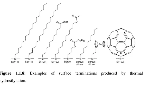
Hydride-terminated Si(100) was shown to react in a similar fashion.38 Working at 200 °C, a number of different olefins were examined for their propensity to form stable monolayers. Examples of surface terminations accessible through the thermal hydrosilylation route are shown in Figure 1.1.8.
19
Figure 1.1.8: Examples of surface terminations produced by thermal hydrosilylation.
A 2 h contact time produced closely packed monolayers when long-chain aliphatic alkenes (12-18 carbons) were used as judged by X-ray reflectivity. A major limitation of the thermal hydrosilylation approach is the large excess of alkene required. For instance, up to several milliliters of neat alkene are required to modify the entire surface of a silicon parallelepiped (50x10x1 mm3). While simple alkenes such as 1-hexadecene are not particularly expensive, for more exotic molecules and for those which are not commercially available and need to be synthesized this point is potential limitation. To circumscribe this restriction, a range of alkenes dissolved in inert, high-boiling hydrocarbons were examined. 1-Hexadecene (10%) in solvents such as n-decane, anisole, toluene, xylene, cumene,
tert-butylbenzene, and mesitylene was compared with the results obtained with
neat 1-hexadecene, the reference sample. The apparent advantage of mesitylene as opposed to the other high-boiling solvents tried is that the use of this molecule does not result in pinhole defects in the monolayer as a result of its large size, as
20
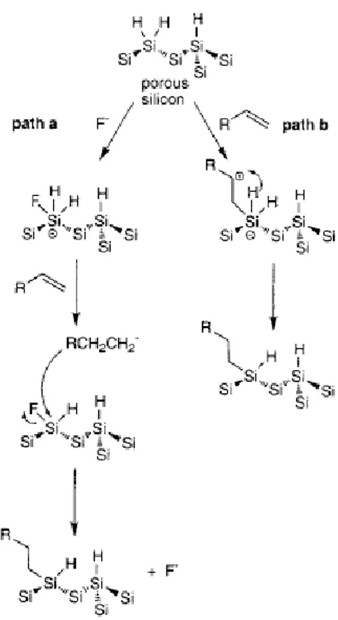
opposed to n-hexadecane which intercalates into the forming monolayer. This work is very useful because it reveals that even dilute solutions of alkene (2.5%) in mesitylene, a 40-fold reduction in absolute quantity, can result in ordered monolayers via thermal hydrosilylation; neat alkene is, therefore, not required. Thermally induced hydrosilylation of alkenes and alkynes has been applied to Si-H-terminated porous silicon surfaces.39,40 Investigations of thermal hydrosilylation
of 1-decene on porous silicon showed that before and after the thermal hydrosilylation the nanoscale structure of the porous silicon skeleton is not affected by the high temperatures and extended time of the reaction. The surfaces are chemically robust, as indicated by a range of chemically demanding conditions, including sonication and boiling in chlorinated solvents, boiling protic acid and base, long-term aqueous HF immersion, and steam treatment. Other mechanisms have been proposed as alternatives to a radical-based reaction, as outlined in figure 1.1.9.41 The ‘standard’ radical mechanism is shown in Figure 1.1.9 b, which is initiated by Si-H bond homolysis or an adventitious radical remaining from the etching process. The first alternative mechanism proposed (path a) involves F -catalysis, since residual fluoride from the etching is always present. Nucleophilic attack of a surface silicon atom by F- results in a pentavalent intermediate which could transfer a hydride to the double bond to give the carbanion. This carbanion then attacks the polarized Si center (δ+Si-Fδ-), releasing F- and forming the Si-C bond. The second alternative mechanism (path b) is based on the ð-electron-rich double bond attacking a surface silicon atom in a nucleophilic center to form a pentavalent silicon atom, followed by hydride transfer (a [1,3] shift) to the carbocation.
21
Figure 1.1.9: Two alternative mechanisms to the radical based mechanism proposed for thermal hydrosilylation.
It is known in the organic and organometallic literature that UV irradiation can promote hydrosilylation of unsaturated compounds41 due to homolytic cleavage of Si-H bonds, as is the case with thermal induction. UV photoinduction, however, takes place at room temperature and thus provides a way to avoid thermal input that could be harmful to delicate or small features on a silicon chip. Minimal input of thermal energy would be preferable in any IC manufacturing process (thermal budget). Irradiation of a hydride-terminated Si(111) surface with UV light (185 and 253.7 nm) in the presence of an aliphatic alkene like 1-pentene or 1-octadecene
22
brings about hydrosilylation in 2 h at room temperature, as shown in figure 1.1.10.42
Figure 1.1.10: Schematic for UV-mediated alkene hydrosilylation on Si(111)-H.
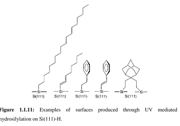
A range of alkenes and alkynes were successfully tried, including octene, 1-octadecene, 1-octyne, styrene, and phenylacetylene, with the alkenes yielding alkyl monolayers and the alkynes yielding alkenyl monolayers; examples of surfaces prepared are shown in Figure 1.1.11.
23
Figure 1.1.11: Examples of surfaces produced through UV mediated hydrosilylation on Si(111)-H.
The mechanism proposed is radical based, with homolytic Si-H bond cleavage initiating the reaction to form a silicon radical (dangling bond),43 similar to that shown in Figure 1.1.7 b.42 Because silicon radicals are known to react very rapidly with unsaturated carbon-carbon bonds,44 Si-C bond formation is expected to be a facile step, forming the surface-bound carbon-based radical on the β-carbon. In contrast to flat, hydride-terminated silicon surfaces, simple reactions can induce hydrosilylation of alkenes and unconjugated alkynes on Si-H-terminated photoluminescent porous silicon surfaces at room temperature in minutes. Some examples of very efficient reactions starting from Si–H terminated porous surfaces are outlined in figure 1.1.12
24
Figure 1.1.12: Some of the surface chemical reactivity of porous silicon.19
From this incredible body of research, many generalizations can now be made about the organometallic surface chemistry of silicon. The field is an extremely exciting one because of the close proximity between fundamental science and technological applications, and it is only a matter of time and circumstance before tailored organic interfaces reach their commercial potential.
25
1.2 Chemical Sensors
All over the world, billions of dollars are spent annually on chemical/biological detections related to medical diagnosis, environmental monitoring, public security and food safety because lab analysis using expensive equipment is usually cumbersome and time-consuming. Therefore, there has been a pressing societal need for the development of chemo/biosensors for the detection of various analytes in solution and atmosphere, which are both less expensive and simpler to construct and operate. Although considerable progress was made in the past several decades, the chemo/biosensor field remains underdeveloped and at a low level of commercialization because of the lack of alternative strategies and multidisciplinary approaches. Only a few chemo/biosensors for simple analytes have been able to meet commercial requirements with detection sensitivity, selectivity, accuracy and reliability approaching that of experimental equipment. However, the recent developments of novel chemosensory materials and fabrication technologies may provide many potential opportunities for the development of a new generation of chemo/biosensors. Thus, the explorations on chemo/biosensors based on novel sensing concept have attracted growing interest in recent years.45
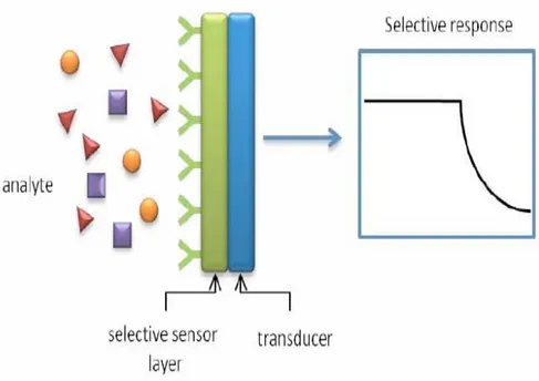
A chemical sensor is a device that transforms chemical information, ranging from the concentration of a specific sample component to total composition analysis, into an analytically useful signal. The chemical information, mentioned above, may originate from a chemical reaction of the analyte or from a physical property of the system investigated.46 The sensing material interacts with the chemical species present in the environment by changing some of its physicochemical properties, while the transducer transforms these variations into a readable signal.
26
Figure 1.2.1: Working principle of supramolecular sensors.
Chemical sensors contain two basic functional units: a receptor part and a transducer part.
In the receptor part of a sensor the chemical information is transformed into a form of energy which may be measured by the transducer.
The transducer part is a device capable of transforming the energy carrying the chemical information about the sample into a useful analytical signal. The transducer as such does not show selectivity.
27
- physical, where no chemical reaction takes place. Typical examples are those based upon measurement of absorbance, refractive index, conductivity, temperature or mass change.
- chemical, in which a chemical reaction with participation of the analyte gives rise to the analytical signal.
- biochemical, in which a biochemical process is the source of the analytical signal. Typical examples are microbial potentiometric sensors or immunosensors. They may be regarded as a subgroup of the chemical ones. Such sensors are called
biosensors.
Chemical sensors may be classified according to the operating principle of the transducer.47
Optical devices transform changes of optical phenomena, which are the result of an
interaction of the analyte with the receptor part. This group may be further subdivided according to the type of optical properties which have been applied in chemical sensors.
Electrochemical devices transform the effect of the electrochemical interaction
analyte-electrode into a useful signal. Such effects may be stimulated electrically or may result in a spontaneous interaction at the zero-current condition.
Electrical devices based on measurements, where no electrochemical processes
take place, but the signal arises from the change of electrical properties caused by the interaction of the analyte.
Mass sensitive devices transform the mass change at a specially modified surface
into a change of a property of the support material. The mass change is caused by accumulation of the analyte.
28
Magnetic devices based on the change of paramagnetic properties of a gas being
analysed. These are represented by certain types of oxygen monitors.
Thermometric devices based on the measurement of the heat effects of a specific
chemical reaction or adsorption which involve the analyte. In this group the heat effects may be measured in various ways, for example in the so called catalytic sensors the heat of a combustion reaction or an enzymatic reaction is measured by use of a thermistor.
Sensors are typically characterized by three properties: sensitivity, selectivity and
reversibility.
Sensitivity can be generally defined as the slope of the analytical calibration curve,
that is correlated with the magnitude of the change in the sensor signal upon a certain change in the analyte concentration.48 “Cross sensitivity” hence refers to the contributions of other than the desired compound to the overall sensor response.
Selectivity is instead the ability of a sensor to respond primarily to only one
chemical species in the presence of other species (usually denoted interferents). The quest for better selectivity remains the cornerstone of the chemical sensing research:49 it can be achieved by using biosensors (e.g. biologically derived selectivity by appropriate enzymes, structure-binding relationship in antibody-antigen complexes,) or by synthesizing materials containing specific binding sites.
Reversibility describes the sensor’s ability to return to its initial state after it has
been exposed to chemical species. The reversibility requires the involvement of weak interactions, since the formation of covalent or ionic bonds would result in an irreversible saturation of the layer.50
29
The conventional design of chemical sensors uses a “lock-and-key” approach (a steric fit concept enunciated for the first time by Emil Fischer in 1894),51 wherein a specific receptor is synthesized to bind the analyte strongly and selectively.
This concept has been widely exploited by supramolecular chemists for the design and synthesis of molecular receptors which are useful to understand and mimic nature specific interactions. As for biological systems, the concepts of shape recognition and binding site complementarity are central for effective molecular recognition in artificial host-guest systems. The progress made in the designing synthetic receptors52 allows sensor selectivity modulation towards different classes of compounds by mastering the weak interactions that occur between the sensing material and the analytes. The selective binding of a neutral substrate by a molecular receptor to form a complex (molecular recognition) is based besides on shape complementarity also on the presence of specific interactions such as hydrogen bonding,53 π-π stacking,54 and CH-π interactions.55 The direct translation of the molecular recognition properties of a given receptor from solution to the solid-gas interface is not trivial, since non-specific interactions such as dispersion forces and material properties such as surface morphology and layer permeability come into play. Molecular recognition is a conceptually attractive and potentially powerful approach to engineering structures and devices at the molecular scale.56 Organic monolayers hosted on inorganic surfaces57-62 represent the best approach for harnessing the full potential of molecular recognition on surfaces.63,64 Compared to both thin films and bulk materials containing molecular receptors, such hybrid organic-inorganic materials have the advantage of reducing or even eliminating non-specific interactions which often mask the recognition events.65 There are a wide choice of host-guest system, such as crown ethers, cavitands, cyclodextrins and calixarenes, very promising.
30
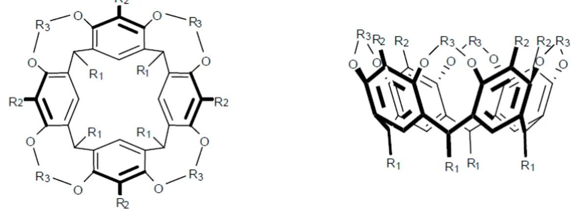
1.3 Cavitands
Interesting and versatile molecular receptors are cavitands, originally defined by Cram as “synthetic organic compounds with enforced concave cavities large enough to complex complementary organic molecules or ions”66, whose complexation properties have been extensively studied in the solid state67, in solution68 and in the gas phase.
The concave surface permits the positioning of different functional groups on the substrate binding site that is usually located inside the cavity.69
Figure 1.3.1: Structure of a cavitand top (left) and side(right) views.
Cavitands are generally synthesized by covalent linkage of neighboring phenolic hydroxyl groups in the corresponding octols. They are particularly attractive because the rim of the bowls can be varied by different R2 substituent and bridging
groups R3 for deepening the bowl cavity and for introducing potentially
cooperating functional groups to act as molecular receptors.70 Moreover the R1
substituent can be use for manipulating the solubility or the morphology in the solid state. The cavitands are designed to bind target molecules to form host-guest complexes with a variety of guest molecules and ions through their rigid, concave
31
π- basic cavity, which enables electrostatic interactions such as cation-π and CH-π and in addition, appropriate substitution at the upper-rim allows them to employ hydrogen bonding in the formation of complexes.
The most common bridging groups are alkylenedioxy, dialkylsilicon, heterophenylene and phosphoryl.
In this thesis we focalized the attention on three classes of cavitands for applications as sensors: phosphourus-bridged, quinoxaline-bridged and acid-bridged cavitands.
1.3.1 Quinoxaline-Salen-bridged cavitands
The cavity of resorcinarenes can be largely extended by bridging phenolic hydroxyl groups with aromatic spacers.71Tetraquinoxaline cavitands result from nucleophilic aromatic substitution with 2,3-dichloroquinoxaline on the phenolic oxydryl moieties of a resorcin[4]arene.
A particularly interesting properties of these systems is the reversible switching between a closed “vase” conformation with a deep cavity for guest complexation, and an open “kite” conformation with a flat extended surface.72 Indeed the quinoxaline spacers can occupy either axial (a) or equatorial (e) positions (Figure 1.3.2). In the “vase” (aaaa) conformer, the spacers touch each other via their α-hydrogens while forming a box like cavity with C4V symmetry which is approximately 7 Å wide and 8 Å deep.73. The cavity is open at the top and closed at
the bottom by the cavitand itself. In the “kite” (eeee) conformer, the spacers are more or less in the same plane (C
2v symmetry). Conformational switching can be
reversibly induced by temperature or pH changes, with the “kite” conformation being preferred at low temperatures and low pH values, or by metal-ion addition.
32
Figure 1.3.2: Structure of quinoxaline cavitand aaaa conformer (left) and eeee conformer (right).
In contrast, in mixed-bridged cavitands with one of the four quinoxaline wings displaced by a different bridge, the thermal vase-to-kite interconversion is switched off by substantially decreasing the solvation of the kite form. Mixed-bridged cavitands can only adopt the kite conformation by protonation of the quinoxaline nitrogen atoms with an acid such as TFA, as a result of the developing Coulombic repulsion in the vase geometry.
New mixed-bridged triquinoxaline (3QxCav) are proposed as receptor for the realization of materials to be used as trapping devices for nitroaromatic compounds.
The receptor discussed in this thesis consists of a 3QxCav compound functionalized with a, N,N-bis(salicylaldehyde) ethylenediimine (salen) functionality. In this receptor, in addition to CH-π interactions between the analytes and the cavity bottom and walls, the presence of the chiral salen allow a chiral discrimination. Chiral salen-metal complex act as a heteroditopic receptor in which the metal centre is able to coordinate the anion, whereas the π-rich
33
quinoxalinic cavity binds tetraalkylammonium cations by stabilizing them with CH···π and cation···π interactions.
1.3.2 Phosphorous bridged Cavitands
The first attempt to synthesize phosphorous-bridged cavitands was carried out in Cram’s group in the 1980s by reacting a methyl-footed resorcin[4]arene with dichlorophenylphosphonate, obtaining a mixture of diastereomers difficult to isolate.74
In fact, the presence of four PV stereogenic centers gives rise to six possible diastereomeric cavitands. The inward (i) and outward (o) configurations are defined relative to the different orientation of the P=O moieties (Figure 1.3.3)
34
The tetraphosphonate cavitands nomenclature, reported in Figure 1.3.3, summarizes the number and relative positions of PVbridges, their stereochemistry, and the type of substituents at the lower rim, at the apical positions, and on the phosphorus bridges, respectively, in a single term.
In particular, the capital letter, defines number and nature of bridges, the lower case letters define the in-out stereochemistry, and R 1, R2 and R3 in brackets define the substituents at the lower rim, in the apical positions and on the phosphorous stereocenters respectively.
Tetraphosphonate cavitand presents remarkable recognition properties toward N-methylammonium (K
ass∼10 9
, Figure 1.3.4 a) and N-methylpyridinium (Kass∼107 Figure 1.3.4 b) which can be attributed to three synergistic interaction
modes:
(i) N+•••O=P cation-dipole interactions;
(ii) CH3-π interactions of the acidic +N-CH3 group with the π basic cavity;
(iii) two simultaneous hydrogen bonds between two adjacent P=O bridges and the two nitrogen protons,75 in the case of protonated secondary amines;
The simultaneous hydrogen bonds are the reason for the higher affinity of the N-methylammonium toward the cavity.
35
Figure 1.3.4: Interactions involved in the molecular recognition process.
Another class of cavitand (TS
iiii), structurally identical to the Tiiii receptor except
for the presence of four P=S instead of four P=O has been synthesized via oxidation in situ of the tetraphosphonite cavitand with S
8.
This substitution strongly reduces the molecular recognition properties, because sulphur has lower electronic density with respect to the oxygen and consequently less affinity for H-bonding interactions.22 In addition the cavity of TSiiiiis much smaller and less prone to guest inclusion because sulphur is larger (atomic radius=1 Å) than oxygen (atomic radius=0.6 Å). (Figure 1.3.5)
36
Figure 1.3.5: Comparison between tetraphosphonate and tetrathiophosphonate cavitands (top view).
37
1.4 References
1 J. Gao, B. Xu, Nano Today, 2009, 4, 37-51.
2 L. Zhang, T. J. Webster, Nano Today, 2009, 4, 66-80.
3 a) C. Bae, H. Yoo, S. Kim, K. Lee, J. Kim, M. M. Sung, H. Shin, Chem. Mater.
2008, 20, 756–767. b) G. R. Patzke, F. Krumeich, R. Nesper, Angew. Chem., Int.Ed. 2002, 41, 2446–2461. c) S. J. Hurst, E. K. Payne, L. Qin, C. A. Mirkin, Angew. Chem., Int. Ed. 2006, 45, 2672–2692. d) B. Tian, T. J. Kempa, C. M. Lieber, Chem. Soc. Rev. 2009, 38, 16–24.
4 Y. Qiu, P. Chen, M. Liu, J. Am. Chem. Soc., 2010, 132, 9644-9652. 5 New Scientist 1983, 98, 20.
6 L. Netzer, J. Sagiv, J. Am. Chem. Soc. 1983, 105, 674.
7 W. C. Bigelow, D. L. Pickett,W. A. Zisman, J. Colloid Sci. 1946, 1, 513. 8 W. C. Bigelow, E. Glass, W. A. Zisman, J. Colloid Sci. 1947, 2, 563.
9 E. E. Polymeropoulos, J. Sagiv, J. Chem. Phys. 1978, 69, 1836. 10 J. Sagiv, J. Am. Chem. Soc. 1980, 102, 92.
11 S. Onclin, B. J. Ravoo, D. N. Reinhoudt, Angew. Chem. Int. Ed. 2005, 44, 6282-6304.
12 J. C. Love, L. A. Estroff, J. K. Kriebel, R. G. Nuzzo, G. M. Whitesides, Chem. Rev. 2005, 105, 1103-1169.
38
13 C. Tidwell, S. Ertel, B. Ratner, B. Tarasevich, S. Atre, D. Allara, Langmuir 1997, 13, 3404-3414.
14 R. E. Holmlin, X. Chen, R. G. Chapman, S. Takayama, G. M. Whitesides, Langmuir, 2001, 17, 2841-2850.
15 E. Ostuni, R. G. Chapman, M. N. Liang, G. Meluleni, G. Pier, D. E. Ingber, G. M. Whitesides, Langmuir, 2001, 17, 6336-6343.
16 C. Engtrakul, L.R. Sita, Nano Lett., 2001, 1, 541-549.
17 J. J. Gooding, F. Mearns, W. Yang, J. Liu, Electroanal., 2003, 15, 81-96. 18 M. Kind, C. Woll Progress in Surface Science, 2009, 84, 230–278. 19 J. M. Buriak, Chem. Rev. 2002, 102, 5, 1271-1308.
20 L. T. Canham, Properties of porous silicon. 1997, London: Inspec. 21 M. J. Sailor, E. J. Lee, 1997 Adv. Mater. 9, 783.
22 A. G. Cullis, L. T. Canham and P. D. J. Calcott, J. Appl. Phys., 1997, 82, 909. 23 A. Halimaoui, in Properties of Porous Silicon, ed. L. T. Canham, INSPEC,
London, 1997, p.12.
24 M. T. Kelly, J. K. M. Chun, A. B. Bocarsly, Appl. Phys. Lett., 1994, 64, 1693. 25 N. Noguchi, I. Suemune, Appl. Phys. Lett., 1994, 62, 1429; O. K. Anderson, T.
Frello and E. Veje, J. Appl. Phys., 1995, 78, 6189.
39
27 G. S. Higashi, R. S. Becker, Y. J. Chabal, A. J. Becker, Appl. Phys. Lett., 1991,
58, 1656.
28 A. Bansal, X. Li, I. Lauermann, N.S. Lewis, J. Am. Chem. Soc. 1996, 118, 7225. 29 A. Bansal, X. Li, S.I. Yi, W.H. Weinberg, N.S. Lewis, J. Phys. Chem. B, 2001,
105, 10266.
30 X.-Y. Zhu, V. Boiadjiev, J.A. Mulder, R.P. Hsung, R.C. Major, Langmuir, 2000,
16, 6766.
31 B.J. Eves, G.P. Lopinski, Surf. Sci. 2005, 579, L89.
32 D. Narducci, L. Pedemonte, G. Bracco, Appl. Surf. Sci. 2003, 212, 649.
33 L. Pedemonte, G. Bracco, A. Relini, R. Rolandi, D. Narducci, Appl. Surf. Sci.
2003, 212, 595.
34 J.M. Lauerhaas, M.J. Sailor, Science, 1993, 261, 1567. 35 V.T. Joy, D. Mandler, Chem. Phys. Chem. 2002, 3, 973. 36 J. M. Buriak, Chem. Commun., 1999, 1051-1060.
37 C. Chatgilialoglu, Acc. Chem. Res., 1992, 25, 188.
38 A. B. Sieval, A. L. Demirel, J. W. M. Nissink, M. R. Linford, J. H. van der
Maas, W. H. de Jeu, H. Zuilhof, E. J. R. Sudhölter, Langmuir 1998, 14, 1759.
39 R. Boukherroub, S. Morin, D. D. M. Wayner, F. Bensebaa, G. I. Sproule, J.-M.
40
40 J. E. Bateman, R. D. Eagling, B. R. Horrocks, A. Houlton, J. Phys. Chem. B
2000, 104, 5557.
41 R. Boukherroub, S. Morin, D. D. M. Wayner, F. Bensebaa, G. I. Sproule, J.-M.
Baribeau, D. J. Lockwood, Chem. Mater. 2001, 13, 2002.
42 R. L. Cicero, M. R. Linford, C. E. D. Chidsey, Langmuir 2000, 16, 5688. 43 C. A. Burkhard, R. H. Krieble, J. Am. Chem. Soc. 1947, 69, 2687.
44 J. M. Kanabus-Kaminska, J. A. Hawari, D. Griller, C. Chatgilialoglu, J. Am.
Chem. Soc. 1987, 109, 5267-5268.
45 G. Guan, B. Liu, Z. Wang, Z. Zhang Sensors 2008, 8, 8291-8320.
46 A. Hulanichì, S. Geab, F. Ingman, Pure&App. Chern., Vol. 63, No. 9, pp. 1247-1250, 1991.
47 R. W. Cattrall, Chemical Sensors, Oxford Science Publications, 1997. 48 A. D’Amico, C. Di Natale, IEEE Sensors Journal 2001, 1, 183. 49 J. Janata, M. Josowicz, Anal. Chem. 1998, 70, 179.
50 A. Hierlemann, A. J. Ricco, K. Bodenhöfer, W. Göpel, Anal. Chem. 1999, 71, 3022.
51 E. Fischer, Ber. Dtsch. Chem. Ges. 1894, 27, 2985.
52 J.-M. Lehn, Supramolecular Chemistry, Wiley-VCH, Wienheim, 1995. 53 J. Rebek, Angew. Chem. Int. Ed., Engl., 1990, 29, 245-255.
41
54 C. H. Hunter, K. R. Lawson, J. Perkins, C. J. Urch, J. Chem. Soc., Perkin Trans. 2001, 2, 651-699.
55 M. Nishio, M. Hirota, Y. Umezawa, The CH-π Interactions, Wiley-VCH, New-York, 1998.
56 G. M. Whitesides, B. Grzybowski, Science, 295, 2418.
57 M. Dubey, S. L. Bernasek, J. Schwartz, J. Am. Chem. Soc. 2007, 129, 6980–
6981.
58 S. Zhang, C. M. Cardona, L. Echegoyen, Chem.Commun. 2006, 4461–4473. 59 A. Facchetti, E. Annoni, L. Beverina, M. Morone, P. Zhu, T. J. Marks, G. A.
Pagani, Nat. Mater. 2004, 3, 910–917.
60 Z. Liu, A. A. Yasseri, J. S. Lindsey, D. F. Bocian, Science 2003, 302, 1543– 1545.
61 M. Altman, A. D. Shukla, T. Zubkov, G. Evmenenko, P. Dutta, M. E Van der
Boom, J. Am. Chem.Soc. 2006, 128, 7374–7382.
62 T. Gupta, M. E. Van der Boom, J. Am.Chem. Soc. 2006, 128, 8400–8401.
63 A. B. Descalzo, R. Martìnez-Màòez, F. Sancenòn, K. Hoffmann, K. Rurack,
Angew. Chem., Int. Ed. 2006, 45, 5924–5948.
64 C. Lagrost, G. Alcaraz, J.-F. Bergamini, B. Fabre, I.Serbanescu, Chem. Commun. 2007, 1050–1052.
65 M. Tonezzer, M. Melegari, G. Maggioni, R. Milan, G. DellaMea, E. Dalcanale,
42
66 D. J. Cram, J. M. Cram, In Container Molecules and Their Guests (ED.: J. F. Stoddart), The Royal Society of Chemistry, Cambridge, 1994, Chapter 5.
67 D. J. Cram, S. Karbach, H.-E. Kim, C. B. Knobler, E. F. Maverick, J. L. Ericson, R. C. Helgeson, J. Am. Chem. Soc. 1988, 110, 2229-2237.
68 a) J. A. Tucker, C. B. Knobler, K. N. Trueblood, D. J. Cram, J. Am. Chem. Soc.
1989, 111, 3688-3699. b) P. Soncini, S. Bonsignore, E. Dalcanale, F. Ugozzoli, J. Org. Chem. 1992, 57, 4608-4612. c) T. Haino, D. M. Rudkevich, A. Shivanyuk, K. Rissanen, J. Rebek, Jr., Chem. Eur. J. 2000, 6, 3797-3805. d) K. Paek, J. Cho, Tetrahedron Lett. 2001, 42, 1927-1929.
69 A. Friggeri, F.C.J.M. Van Veggel, D.N. Reinhoudt, Langmuir 1998, 14, 5457-5463.
70 P. Timmerman, W. Verboom, D. N. Reinhoudt, Tetrahedron 1996, 52, 2663.
71 a) J.R. Moran, S. Karbach, D.J. Cram J. Am. Chem. Soc. 1982, 104, 5826; b)
J.A. Bryant, J.L Ericson, D.J. Cram J. Am. Chem. Soc. 1990, 112, 1255; c) D.J. Cram, H.–J. Choi, J.A. Bryant, C.B. Knobler, J. Am. Chem. Soc, 1992, 114, 7748.
72 P. Roncucci, L. Pirondini, G. Paderni, C. Massera, E. Dalcanale, V.A. Azov, F.
Diederich, Chem. Eur. J. 2006, 12, 4775.
73 E. Dalcanale, P. Soncini, G. Bacchilega, F. Ugozzoli, J. Chem. Soc. Chem.,
Chem. Commun 1989, 500.
43
75 J. J. Lundquist, T. E. Toone, The Cluster Glycoside Effect, Chem. Rev. 2002, 102, 555-578.
44
Chapter 2
Flat-Silicon grafting of Tetraphosphonate
cavitand for molecular recognition:
From Sensing to Nanoengineering of functional
molecules.
2.1 Introduction
Among the several surface functions identified to be worth pursuing, molecular recognition is particularly noteworthy for its profound impact on biology and materials science. In living organisms, multiple recognition events trigger the immune system response through antibodies, and they promote the adhesion of viruses on cell surfaces.1 A strong contribution to the development of molecular recognition themes was given by supramolecular chemistry. In the last decades, researchers active in this field have designed and prepared an amazing number of different synthetic receptors aimed either at the recognition of target molecules2-4
45
or at the fabrication of well-defined 2D and 3D molecular assemblies at interfaces,5,6 through non-covalent interaction.
Tetraphosphonate cavitands are particularly versatile synthetic receptors: their complexation ability span from positively charged inorganic and organic species7
to neutral molecules8. This diverse complexation ability is the result of three
interaction modes, which can be activated either individually or in combination by the host according to the guest requirements: (a) multiple ion-dipole interactions between the inward facing P=O groups and the positively charged guests9; (b) single or dual H-bonding involving the P=O groups9,10; and (c) CH3-π interactions
between a methyl group present on the guest and the cavity of the host11.
The complexation properties of tetraphosphonate cavitands anchored on silicon surface toward N-methyl pyridinium and N-methyl ammonium salts in organic solvents have been recently investigated12. In the present chapter I use the tetraphosphonate cavitands to distinguish between N-methylated amino acids and their non-methylad analogues and I explored the possibility to transfer their complexation properties to aqueous and biological environments. Moreover the combination of the molecular recognition properties of cavitands with the metal-coordination ability of specific guests allowed the development of a self-assembly protocol to build luminescent coordination structures on silicon.
2.1.1 Molecular recognition of N-methylated amino acids: sarcosine
detection as tumoral marker
Prostate cancer is the most common cancer in men, with 913,000 new cases diagnosed and 258,000 related deaths worldwide in 200813. Due to its large incidence, it is the second leading cause of cancer-related death among the male population in the United States14 and in the European Union15. The traditional diagnosis, based on prostate specific antigen (PSA), does not distinguish between
46
aggressive and slow-growing cancer forms. In particular, it is important to differentiate the organ-confined disease from the aggressive metastatic one. This distinction is essential to guarantee the earliest treatment in the worse cases and to avoid unnecessary surgeries in the others. Early stage detection of aggressive prostate cancer has been recently linked to the presence of sarcosine in urine.15
Sarcosine forms when the enzyme glycine-N-methyltransferase transfers a methyl group from S-adenosylmethionine to glycine. Being sarcosine one of the cancer biomarker candidates 16,17, effective diagnostic tools for the detection of sarcosine directly in urine are highly desirable. The basic methodology for sarcosine determination is gas chromatography-mass spectroscopy which, although highly sensitive and reliable, is hardly applicable for a widespread screening of this pathology. A different approach for sarcosine determination consists in the use of a fluorometric assay (BioVision Research Products, Mountain View, CA). However, it requires various reaction steps and it is prone to interference due to unspecific reactions with other (unknown) urinary analytes16, making it unsuitable for sarcosine measurements directly in the urine. A diffuse screening of prostate cancer requires easy and fast methodologies which point to minimize sample manipulations, number of reagents and costs. An important step in this direction could be the development of an interactive surface akin to DNA chips, able to perform the recognition process directly in biological fluids.
In chemical terms, the preparation of a sarcosine detection chip requires: (i) the design of a receptor capable to bind exclusively N-methylated amino acids in the presence of overwhelming amounts of amino acids plus many other metabolites in urine (ii) the grafting of this receptor on a suitable solid surface, retaining the molecular recognition properties at the solid-liquid interface. In this context, in this thesis, I focused on a comprehensive investigation of the molecular recognition
47
properties of a phosphonate cavitand-functionalized silicon surface toward glycine and sarcosine in water and urine.
2.1.2 Hierarchical Self-Assembly of luminescent systems
The design and synthesis of functional material are of current interest in chemistry and nanoscience.18,19 In particular, self-assembled hybrid materials20-22, held together by different kinds of noncovalent interactions , are particularly intriguing because they lead to adaptive materials,23 characterized by switchable functions. The resulting complexity of these hybrid materials requires implementing combinations of two or more different interaction modes, among which hydrogen bonding, host-guest complexation, and metal-ligand coordination.
The use of luminescence to investigate the properties and functions of supramolecular assemblies has been extensively employed due to its non-invasive nature, fast response time and high sensitivity.24 Luminescence spectroscopy has been finding applications in fields of great impact from a social and economic point of view, such as medical diagnostics and imaging, environmental sciences, and molecular electronics. In this context, luminescence spectroscopy has proved to be a very powerful technique when it is necessary to monitor molecular recognition events in cells or on surfaces, because of its submicron visualization and submillisecond temporal resolution. Furthermore, one can take advantage of the variety of possible ways of modulating the photophysical properties of a chromophore. Starting from this premise, we designed a set of molecules (Figure 2.2.1) featuring one or two binding motifs, to use as “switching modules” to control the self-assembly process in the multistep growth of supramolecular structures on silicon.
48
2.2 General procedures
2.2.1 Synthesis of Tiiii, TSiiii, ammonium salts and lanthanide
complexes
The synthesis of cavitands and methylated guests was carried out at University of Parma by the group of Professor Enrico Dalcanale and was synthesized following a published procedure (Figure 2.2.1).12
The Yttrium complex was purchased by Sigma-Aldrich and Europium complex was synthesized at University of Warszawa.
49
Figure 2.2.1: Chemical structure of guests and cavitands. The short chain footed Tiiii[C3H7, CH3, Ph] cavitand was used for solid state and solution experiments.
The double bond-terminated long chain footed Tiiii[C10H19, CH3, Ph]
TSiiii[C10H19, H, Ph] and MeCav cavitands were grafted on silicon wafers.
2.2.2 Synthesis of Tiiii
To a solution of resorcinarene25 (1g, 0.91mmol) in freshly distilled pyridine (10 mL) dichlorophenylphosphine (0.504 mL, 3.72 mmol) was added slowly, at room temperature. After 3 hours of stirring at 80 °C, the solution was allowed to cool at
MeCav R=C10H19 3 4 5 Eu CF3 F3C O O F3C CF3 O O CF3 CF3 O O H2O H2O N N N H H2N O CH3 Cl Y CF3 F3C O O F3C CF3 O O CF3 CF3 O O H2O H2O
50
room temperature and 4mL of 35% H2O2 was added. The resulting mixture was
stirred for 30 min at room temperature, then the solvent was removed under reduced pressure and water added. The precipitate obtained in this way was collected by vacuum filtration, and profusely rinsed with diethyl ether to give the product in a quantitative yield.
2.2.3 Preparation of Tiiii-grafted Si surface (Si-Tiiii)
For grafting monolayers, a Tiiii/1-octene mixture (χcav = 0.05) were dissolved in
mesitylene (solution concentration = 50mM), the use of the 1-octene spacer improves the passivation of the silicon surface, thus minimizing the substrate oxidation after aging.12 Cavitand solutions (2.0 mL) were placed in a quartz cell and deoxygenated by stirring in a dry box for at least 1 h. A Si(100) substrate was dipped in H2SO4/H2O2 (3:1) solution for 12 min to remove organic contaminants,
then it was etched in a hydrofluoric acid solution (1% v/v) for 90 s and quickly rinsed with water. The resulting hydrogenated silicon substrate was immediately placed in the mesitylene solution. The cell remained under UV irradiation (254 nm) for two hours. The sample was then removed from the solution and sonicated in dichloromethane for 10 min to remove residual physisorbed material.
2.2.4 Monolayer Characterization
XPS spectra were run with a PHI 5600 multi-technique ESCA-Auger spectrometer equipped with a monochromated Al Kα X-ray source. Analyses were carried out with a photoelectron angle of 45° (relative to the sample surface) with an acceptance angle of ± 7°. The XPS binding energy (B.E) scale was calibrated by centering the C 1s peak due to hydrocarbon moieties and “adventitious” carbon at 285.0 eV.26