Università degli Studi di Catania
Dottorato di Ricerca in Scienze dei Materiali
XXV Ciclo
R. M. Gabriella Milazzo
ELECTROLESS SILVER DEPOSITION ON
(100) AND (111) SILICON WAFERS,
FABRICATION OF NANOWIRES AND
NANOPILLARS BY ASSISTED ETCHING
Tutor:
Prof. E. Rimini
Prof.ssa M.G. Grimaldi
Supervisor:
Dr. G. D’Arrigo
Coordinatore: Prof. A. Licciardello
“In small proportions we just beauties see, And in short measures life may perfect be”
i
CONTENT
INTRODUCTION p. 1
CHAPTER 1
Phenomenology of Metal Assisted Etching of Silicon 5
1.1 Metal Deposition 8
1.1.1 General Concepts 8
1.1.2 Electroless Metal Deposition (EMD) 9
1.1.3 Electroless Silver Deposition 10
1.1.4 Growth of Silver clusters on Silicon 12 1.1.5 Investigation of Silver Nanoparticles (AgNPs)
growth 13
1.2 Silver Assisted chemical Etching 22
1.2.1 The system Ag-Si-H2O2-HF 22
ii
1.4 Factors influencing MAcE 26
1.4.1 Temperature 26
1.4.2 Illumination 27
1.4.3 Doping type and level 28
1.5 Metal Patterning for MAcE applications 29
1.5.1 Nanospheres Lithography 30
1.5.2 AAO Mask Method 33
1.5.3 Interference Lithography Method 35
1.5.4 Block-Copolymer Lithography 36
CHAPTER 2
Electroless Silver Deposition on (100) and (111) Silicon Substrates 39
2.1 Influence of substrate morphology 40
2.2 Silver Deposition on individual Si(100) and Si(111) 42
2.2.1 Experiments 42
2.2.2 Results 43
2.2.3 Consideration about the orientation dependence of Electroless Ag Deposition 50 2.3 Silver Deposition on macro-patterned Si wafers: simultaneous
iii
exposure of contiguous (100) and (111) surfaces 52 2.3.1 Fabrication of macro-patterned Si 52 2.3.2 A brief overview on KOH etching of Si 53 2.3.3 Morphological characterization
of macro-patterned Si 56
2.3.4 Silver Deposition on macro-patterned Si 59
2.3.5 Results 60
2.4 Discussion 64
2.4.1 H-Terminations Role 64
2.4.2 The role of surface microstructure 65
2.4.3 The Mass Transport influence 69
CHAPTER 3
Influence of Metal morphology on the etching direction and application in
Silicon Nanopillars fabrication 73
3.1 The orientation dependent behavior of MAcE 73 3.1.1 Dependence on the etching solution composition
75 (a) Etching of (100)Si: the dependence on the ratio
iv
(b) Etching directions of non (100)Si 78 3.1.2 The influence of metal morphology 80
3.2 Experiments 85
3.3 Etching of Si(100) and Si(111) 85
3.3.1 Morphological characterization of etched Si(100) and
Si(111) 86
3.3.2 Morphological characterization of etched macro-
patterned Si 92
3.4 Discussion 94
3.5 Application of the achieved metal positioning control for the fabrication of SiNPs: MAcE on micro-patterned Si 99
3.5.1 Fabrication of micro-patterned Si 100 3.5.2 Morphological characterization of micro-patterned Si
100
3.5.3 Experiments 102
CONCLUSION AND FUTURE PROSPECTIVE 109
REFERENCES 111
ACKNOWLEDGEMENTS 117
1
INTRODUCTION
The nanoscience is the study of objects with sizes ranging from a few tenths to one hundreds of nanometers, and nanotechnology deals with the manipulation of nanomaterials to fabricate devices.
Low-dimensional nanomaterials are of particular interest because they exhibit anisotropic and dimension-tunable properties, both of which are important attributes in nanodevice application [1, 3]. Silicon is the mainstay of semiconductor industry and nanostructures such as quantum dots (SiQDs) [4], nanocrystals (SiNCs) [5], porous Si (por Si) [6], Si Nanopillars (SiNPs) [7] and Si nanowires (SiNWs) [8] exhibit interesting properties that are very different from their bulk counterparts [9]: a diameter-dependent bandgap, very high density electronic states, an increased surface-to-volume ratio, an enhanced exciton binding energy, enhanced thermoelectric properties and increased surface scattering for electrons and phonons.
SiNSs are very interesting for application in electronic and photonic devices [10], sensors [11], energy harvesting devices [12], and solar cells [13, 15]. For these reasons, the field of SiNWs synthesis represents an exciting and rapidly expanding research area.
The VLS (Vapor Liquid Solid) method [9], the main growth technique for SiNWs, was proposed by Wagner and Ellis in the mid 1960s and is the key mechanism for silicon wire growth. It relies on the dissolution of gaseous reactants into nanoscaled liquid droplets of metal, followed by nucleation and growth of single crystalline rods in one direction.
When Au, for example, is deposited on a silicon substrate, and this substrate is heated, small liquid Au-Si alloy droplets will form on the
2
substrate surface. When the substrate is exposed to a gaseous silicon precursor, the droplets become supersaturated with Si until silicon freezes out at the silicon droplet interface. The continuation of this process leads to the wire’s growth.
So the globule at the wire tip must be involved in the growth by acting “as a preferred sink for the arriving Si atoms or, perhaps more likely, as a catalyst for the chemical processes involved” [16].
High temperature, hazardous silicon precursors, complex equipment and other rigorous conditions are often required. Moreover the usually adopted growth techniques yield disordered entanglements of nanowires, hampering subsequent experimental characterization and potential applications.
Hence the accurately controlled fabrication of ordered SiNW arrays with the desirable axial orientation using simpler and quicker ways is very desirable and of great importance.
Metal Assisted chemical Etching (MAcE) [17] has been exploited in the last decades as an alternative method for silicon manufacturing thanks to its desirable features. It allows the fabrication of various Si nanostructures with electrical properties directly inherited from the bulk silicon substrate. They are robust and they do not peel off from the substrate. The process could be accomplished in a chemical lab without expensive equipment. MAcE is essentially a wet etching method to produce anisotropic high aspect ratio semiconductor micro and nanostructures without incurring in lattice damage. It has been employed to fabricate Si, Si/Ge [18] and GaAs [19] nanostructures potentially useful in fields ranging from solar energy conversion, thermal power conversion, energy storage and chemical and biological sensing.
The process requires the deposition of a noble metal film on the silicon substrate (by Electroless Metal Deposition, evaporation, physical deposition, etc.). The metal, thanks to its catalytic activity, will locally assist the oxidation of Silicon in oxidative solutions. Hydrofluoridric Acid plays an important role in the whole reaction because it etches the oxidized silicon,
3
allowing the metal dipping and so the nanostructures’ generation.
In spite of the simplicity of experimental apparatus and of the high quality of the obtained nanowires, a detailed theoretical description of MAcE is still missing.
Several factors affect the fabrication of SiNWs, e.g., the doping level and type, the substrate orientation, the temperature, the etchant composition. In addition, the control of position and size of metal agglomerates is an important goal to achieve since the spatial distribution and the diameter of nanowires depend on them. Considerable efforts have been done to solve this question (Nanosphere Lithography, Anodic Aluminum Oxide Mask, Interference Lithography etc. have been employed as masking techniques for metal deposition).
In this thesis, the noble metal mesh has been achieved electrolessy, through immersion of silicon in a solution containing Ag+ and Hydrofluoridric Acid. This method is very simple and inexpensive but in general doesn’t allow an accurate metal positioning. In this work numerous efforts have been done to understand the mechanism responsible for Ag+ nucleation and growth on Si.
In Chapter I, after an overview on the general aspects of MAcE, an investigation on the early stages of silver deposition is presented.
In Chapter II, the mechanism of electroless deposition is presented on both (100) and (111) oriented Si wafers.
By means of a substrate patterned with etching in alkaline solutions, it will be shown that when the two surfaces are contiguous, a self selective mechanism for deposition could be achieved.
It results form a complex combination of non homogeneous surface bond density, variations in the kind of Hydrogen-terminations and mass transport effects
As a result, deposition is enhanced on convex surfaces, where silver is in the form of large clusters and on (100) oriented areas and nearly inhibited on concave surfaces.
4
direction is presented. It will be shown that when silver clusters are small and well separated, etching is not normal to the surface but it proceeds along the [001] directions for both orientations under investigation.
On the other side, large and interconnected particles sink always along the normal to the surface.
In addition, by scaling the pattern obtained with etching in alkaline solutions, an enhancement of the self selective behavior for metal cluster’s nucleation and growth occurred. The non uniform silver particles’ density and size in the micro regions gave rise, after etching, to the fabrication of an ordered array of Si Nanopillars, 600nm in size.
5
CHAPTER 1
PHENOMENOLOGY OF METAL ASSISTED ETCHING OF
SILICON
The first demonstration of Metal Assisted chemical Etching (MAcE) of Si was reported in 1997. Porous Si was fabricated by etching a Si substrate Aluminum covered in a solution composed of HF, HNO3 (Nitric Acid) and
H2O. It was discovered that the incubation time to etch silicon decreased
thanks to the presence of the metal film on the surface [20].
The method was first investigated in some details by Li and Bohn [17]. A thin layer of noble metal (e.g., Au, Pt, Ag), sputtered on silicon surface, catalyzed the etching in a mixed solution containing HF, H2O2 (Hydrogen
Peroxide) and EtOH (Ethanol) by enhancing the silicon oxidation reaction. HF was needed to remove the silicon oxide.
It is a simple and inexpensive technique for the fabrication of porous silicon and it has been also employed in the nano-structuring of other semiconductors: Germanium [18], GaAs [19, 20], GaN [21]and SiC [22] The overall process consists mainly in two steps:
1. Deposition of a noble metal that could be achieved by various method, e.g. evaporation, plating, sputtering, etc.;
2. Etching in a solution containing an oxidative agent (usually H2O2) and HF.
6
The noble metal should assume a discrete distribution on the substrate, e. g. in the form of NPs (Nano Particles), or ordered pattern. It enhances the oxidation process, by the oxidative agent, of silicon underneath it. The oxidized silicon is then removed by HF. The substrate in contact with the metal is etched, generating holes whose conglomeration produces the nanostructures. Their shape and size are determined by the metal mesh features [23]. The process is depicted in fig. 1.1. Various metal configurations are reported: isolated or interconnected islands (a and c), metal films with holes (e and g) and metal pattern (i) together with the corresponding etched structures.
7
Fig.1. 1: A schematic representation of Metal Assisted chemical Etching of Si: (a-c-e-g) Si substrate partly covered with a metal film and (b-d-f-h) corresponding structures after etching of Si underneath. If the metal is an ordered pattern (i),
ordered arrays of nanostructures are obtained (j).
8
solution, metal morphology. The substrate plays also an important role in both described steps. Its orientation and its starting surface morphology influence the metal deposition and so the subsequent etching directions. In this chapter, I will give an overview on the general dynamics of the two aforementioned steps. A detailed description of dependences on the orientation and substrate morphology will be given in chapter 2 and 3 respectively.
1.1 Metal Deposition
1.1.1 General Concepts
Metal deposition could be realized in various ways, e.g., evaporation, sputtering, molecular beam epitaxy or, as in this work, via electrochemical processes.
The chemical deposition involves a reduction reaction with a charge transfer between the metal ion present in the solution and the substrate. The metal deposition on silicon, in general, occurs with nucleation of metallic clusters, growth of them and coalescence, followed by thickening of the layer.
The substrate influences mainly the nucleation and coalescence steps. The cluster formation by deposition of a metal onto a foreign substrate depends on the interaction energy between the adsorbed metal atom and the substrate and on the difference in interatomic spacing between the bulk metal phase and the crystalline substrate.
Three different modes of growth can be identified: layer by layer (Frank-van der Merwe growth), 2D layer deposition followed by the growth of 3D islands (Stranski-Krastanov growth) and 3D island formation (Volmer-Weber growth) [25-27]. The latter is the most frequent mode, due to the weak interaction energy between the adsorbed metal atom and the semiconductor.
9
1.1.2 Electroless Metal Deposition (EMD)
Electroless deposition is a simple method for the deposition of noble metals and it is usually utilized if there is no strict demand on the morphology of the resulting metal layer.
Electroless plating refers to the autocatalytic or chemical reduction of aqueous metal ions and subsequent plating onto a substrate. It is a widely used method to cover the surfaces with a variety of metals such as Cu, Ni, Au, Pt, etc [28].
Electroless Nichel offers unique properties including uniformity of the deposit in deep recesses, bores and blind holes. Electroless Copper deposition is generally applied to improve the lifetime and performance in a corrosive atmosphere and upon exposure to a harsh environment. Electroless gold is currently being used in the fabrication of semiconductors devices, tabs and chips.
The electroless deposition of metals on silicon from fluoride solutions has raised considerable interest, owing to its wide application in microelectronics. The working principle is the galvanic displacement reaction: the reduction of metal ions and the oxidation of Si atoms. Fluoride ions in solution help sustain the reaction by dissolving the silicon substrate as silicon hexafluoride, avoiding the formation of silicon oxide, thus exposing new silicon surface (fig. 1.2).
10
Fig.1. 2: Mechanism of Galvanic displacement of metals on silicon.
It is usually accepted that the metal ions coming in the proximity of the silicon surfaces, capture electrons from the valence band of silicon (holes injection) and deposit in the form of metallic nuclei [29].
The metal deposition in this work has been achieved electrolessly, by immersion of the silicon substrate in an aqueous solution containing 0.005M Silver Nitrate (AgNO3) and 4.8M HF. The results of a detailed
investigation on silver electroless deposition on silicon will be presented in the next paragraphs. Here I review the general concepts laying at the basis of the process.
1.1.3 Electroless Silver Deposition
Electroless silver deposition on a silicon surface from HF/AgNO3 solution is
based on the galvanic displacement reaction, in which two simultaneous processes occur at the silicon surface [30]:
(i) The cathodic reaction (reduction of Ag+
ions) which produces metallic Ag deposits;
11 ) ( 0 s Ag e Ag++ VB− → Eq.1. 1
(ii) The anodic reaction (oxidation of silicon) during which the charges released by the oxidation of silicon atoms are transferred to the sites of silver deposition:
− + + + → + H O SiO H eVB s Si( ) 2 2 2 4 4 O H SiF H HF SiO2 +6 → 2 6 +2 2 Eq.1. 2
As soon as Ag deposition begins, Ag+ ions in the vicinity of the silicon surface capture electrons from the valence band of Si, due to the relative positions of electrochemical potentials [31], (a schematic representation is reported in fig. 1.3) are deposited in the form of nanoscale metallic Ag nuclei.
Fig.1. 3: Scheme of the potential relationship between bands in a Si substrate and standard potentials of various oxidants indicating that during silver electroless
12
The subsequent Ag+ ions approaching the Si surface would be reduced preferentially on initial Ag nuclei sites rather than on bare silicon due to the relatively low-energy barrier for holes at the Ag/Si interface, i.e. the strong catalytic activity of silver for reaction [32].
The present deposition of Ag leads to the growth of silver nuclei by metal on metal deposition [33].
However the chemical reactions do not give us any information about nucleation and growth of Ag particles or Si dissolution [34]. The kinetic of wet catalytic deposition is hard to record and is thus still unclear to date, due to the difficulty of combining in situ HF-contained chemical etching of SiNWs and observation by a transmission electron microscope (TEM) or scanning electron microscope (SEM).
In addition, the charge transfer between Si and the noble metal would be heavily affected by the surface band bending of Si. Since the hole and the subsequent electron transfer for oxidation of Si occurs at the surface of the Si, the surface state of Si is of importance in exploring the etching mechanism [23]. Their influence is still under investigation [35-37].
1.1.4 Growth of Silver clusters on Silicon.
A large number of possible steps are involved in the electroless deposition of silver onto silicon. It has been speculated that, after nucleation, we have [38]:
(i) Diffusion of Ag+ to the silver surface;
(ii) Discharge (after adsorption) of Ag+ to give Silver on Silver; (iii) F- discharge and reaction at Si surface to give SiF6
-2
; (iv) Desorption of SiF62-;
(v) Diffusion of SiF6
away from the surface.
Possible F- diffusion limitation (i.e. removal of oxidized silicon) with the usual adopted etching solution is ignored, since HF concentration is higher
13
than the Ag+ concentration (e.g in the present experiments [HF]/[AgNO3] is
about 103). It does however appear that the overall growth rate is diffusion controlled by silver species. This is based upon the observation that the silver deposition rate can be increased by a factor of about two by stirring the solution.
1.1.5 Investigation on Silver Nanoparticles (AgNPs) growth.
Silver deposition has been investigated in times ranging between 1s and 160s. The starting substrate was Si (100) (P doped ρ=3-5Ω⋅cm), it was cut in squares of 1cm in side and dipped in Diluited Hydrofluoridric Acid Solution (DHF,Hydrofluoridric Acid and Water 1:7). By this treatment, introduced to remove the native oxide, H-terminated surfaces were obtained. Deposition for times shorter than 5s was achieved by gradual immersion of sample in the deposition bath, as depicted in fig. 1.4
Fig.1. 4: Gradual immersion of sample in the plating solution.
The volume of plating solution was chosen to ensure a large reservoir for
1. 5s
2. 4s
3. 3s
4. 2s
5. 1s
14
Ag+ ions (the adopted 50ml solution contains 1.5 x 10²⁰ions that could grow a continuous layer about few μm thick on squares samples of 1cm in side). The as-deposited samples were analyzed with various techniques, in order to obtain a detailed description of silver evolution with time.
• SEM (Scanning Electron Microscopy)
These analyses allowed a direct evaluation of coverage and size distribution of the silver clusters. The magnification was chosen high enough to allow a clear observation of silver nanoparticles and the empty areas surrounding them.
• Rutherford Backscattering Spectroscopy
The samples were analyzed with RBS (Rutherford Backscattering Spectroscopy) of 2.0MeV He+ ions to determine the amount of deposited Ag atoms (in terms of Ag atoms/cm2) with time.
Some samples were also analyzed with cross section TEM (Transmission Electron Microscopy), to evaluate the height of silver clusters
The SEM micrographs of samples are reported in fig.1. 5. They show that just after 1s the formation of Ag islands has been accomplished. The early stages of deposition are characterized by fast nucleation and growth. The corresponding RBS spectra are reported in fig. 1.6.
15
Fig.1. 5: SEM micrographs of samples immersed for (a) 1s; (b) 3s; (c) 5s; (d) 40s; (e) 120s and (f) 160s.
16
In fig. 1.7 the evolution of surface atomic density, as calculated from RBS spectra, is reported. 0 2 4 6 8 40 60 80 100 120 140 160 180 0 2 4 6 8 10 12 x 1016 A to m s /c m 2 Deposition Time [s]
Fig.1. 7: Atomic surface density calculated from RBS spectra (2.0MeV He+ ions).
Deposition is characterized by a fast initial step. The RBS spectra show that in the first two second the highest deposition rate is detected: from 0 to 2s it is about 1016 [atoms/(cm2s)]. From 2s to 5s the deposition rate become one third of the previous value, about 3x10¹⁵ [atoms/(cm2s)]. Then it continues to decrease and from 40s to 160s the variation is one order magnitude lower (4x10¹⁴ [atoms/(cm2s)]. So the deposition rate continuously slows down.
17 0 2 4 6 8 40 60 80 100 120 140 160 180 0,4 0,8 1,2 1,6 x 10¹¹ D e n s it y [ A g N P s x c m -2] Deposition Time [s]
Fig.1. 8: Density of AgNPs as calculated for SEM micrographs elaboration.
During the first seconds (from 1s to 5s) it decreases of a factor 2, going from 1.6 x 10¹¹ [nuclei/cm-2] to 0.8 x 10¹¹ [nuclei/cm-2]. The higher value is found on sample deposited for 1s, probably after this time, the nucleation step has been already accomplished and coalescences take place. The analysis of the silver nuclei density with time indicated that the aggregation rate slows down too. From 1s to 5s, agglomeration of 3 clusters in 1 occurs (0.4 clusters/s are lost). From 5s to 40s a lower aggregation value (about 0.05 clusters/s) is calculated. For longer times, i.e. from 40s to 160, it further decreases. From the elaboration of SEM micrographs the variation of the clusters mean size with deposition time has been calculated, as reported in fig. 1.9.
18 0 2 4 6 8 40 60 80 100 120 140 160 180 2 4 6 8 10 12 14 x 103 M e a n S iz e [ n m 2 ] Deposition Time [s]
Fig.1. 9: Particle mean size vs deposition time
In fig. 1.10 the radius distributions for 1s and 2s deposited samples is reported. 1 2 3 4 5 6 7 8 9 10 11 12 13 14 15 16 17 18 19 0 20 40 60 80 100 120 C o u n ts Radius [nm] 1s 1 2 3 4 5 6 7 8 9 10 11 12 13 14 15 16 17 18 19 0 20 40 60 80 100 120 C o u n ts Radius [nm] 2s
Fig.1. 10 Radius distribution for (a) 1s and (b) 2s immersion time.
The cluster thickness is reported in fig. 1.11. The trend indicates that in the first seconds a quick deposition occurs and the clusters grow both in thickness and in extension. Then when the deposition slows down, particles coalesce and their height grows slowly.
19 0 2 4 6 8 40 60 80 100 120 140 160 180 5 10 15 20 25 30 35 40 45 C lu s te r' s T h ic k n e s s [ n m ] Deposition Time [s]
Fig.1. 11: Fig. 1.9 Evolution of mean thickness for particles with deposition time
The cross sections TEM of fig.1.12 indeed show the occurrence of grain boundaries in the long particles obtained after 160s deposition time (fig. 1.12 b), while those after 40s (fig. 1.12 a) have aspect ratio≅1 (i.e. are nearly round).
Fig.1. 12: Cross section TEM as samples deposited for (a) 40s and (b) 160s. In (b) many grain boundaries are detectable
20 0 5 40 60 80 100 120 140 160 180 0,1 0,2 0,3 0,4 0,5 0,6 0,7 0,8 C o v e ra g e Deposition Time [s]
Fig.1. 13: Covered Area by AgNPs vs deposition time.
A detailed characterization about AgNPs generation and evolution was conducted by [39] on H-terminated (111) p-type Silicon.
The OCPt (Open Circuit Potential vs time) of deposition was acquired and the measured curve is reported in fig. 1.14.
Fig.1. 14: Ocp-t curve by [39]. The electrolyte was 150mL of 1.0 M HF, 0.1 M AgNO3 solution.
21
Therefore, at the early reaction time, the silver deposition is under the kinetic growth process and the amount of silver deposits increased. In between the points denoted b and c, the slowly increased. EOCP with small
fluctuations implies that a thermodynamic quasi-equilibrium or equilibrium condition might control the reaction. From c then, the unchanged EOCP
suggests that the reaction almost ceased. The time location of the aforementioned points depends on the experimental conditions (the volume and the Ag+ concentration of plating solution much higher than those adopted for our experiments) but a clear trend could be identified. With prolonged deposition times (30min) dendritic structures have been observed, as reported in fig. 1.15.
5 µm
5 µm
Fig.1. 15: Dendritic silver clusters achieved after 30min deposition.
Formation of silver dendrites should be considered within the framework of a diffusion limited aggregation model that involves cluster formation by adhesion of a particle via a random path to a selected seed and particle diffusion to stick to the growing structure. In the initial stage, high concentrations of silver salt lead to a reduction-nucleation-growth of silver nanoclusters on multiple locations to form a chain like network. As the
22
reaction continues, the salt concentration decreases and the growth is mainly driven by the reduced surface energy resulting in the formation of dendritic structures [40].
1.2 Silver Assisted chemical Etching
After the electroless deposition step, Metal Assisted chemical Etching is achieved by immersion of the as-deposited substrate in a solution containing H2O2 and HF. The involved reaction and the factors influencing it
are reported in this section.
1.2.1 The system Ag-Si-H2O2-HF.
The silver assisted chemical etching proceeds according to the reactions (eq.1.3a-d). The reduction of H2O2 (eq.1.3a) occurs on the silver surface.
Silicon is oxidized (eq.1.3b), due to injected holes and then etched by HF into H2SiF6 and SiF4 (eq.1.3c-d) [41-43].
a. H2O2 +2H+ +2e− →2H2O
b. Si+2H2O+4h+ →SiO2 +4H+
c. SiO2 +6HF →H2SiF6 +2H2O
d.
SiO
2+
4
HF
→
SiF
4(
g
)
+
2
H
2O
Eq.1. 3
In order to dissolve Si, it is necessary that two conditions must be fulfilled: (i) Electronics holes are available in the proximity of the etched region (ii) A direct contact with the HF electrolyte exists.
23
Two half cell reactions that include cathode and anode reactions would be greatly enhanced at different sites on the metal particle surface. The side of Ag particle facing the etching solution would act as a cathode, which would catalyze H2O2 reduction, consuming H
+
and electrons in the process, while the other side of Ag particle facing the Si would function as the catalyst for Si oxidation, which would generate H+ and electrons. A schematic representation is given in fig. 1.16 [44].
Fig.1. 16: A schematic representation of silver assisted etching a silicon through the reduction of H2O2 on the Ag particle facing the etching solution and removal
of oxidized silicon. The process results in etching of nanopits in silicon.
So the catalythic Ag particles would act as a redox center: electrons are transferred from silicon to silver nanoparticles to reduce H2O2 on the
surface of metal particles facing to the electrolyte. Meanwhile, the metal particles, thanks to HF action on silicon, etch nanopits down into the wafer. Such an electron cycle results in the formation of silicon nanowires arrays. The electrochemical potential of H2O2 is much more positive than the
valence band of Si, from the energy point of view; H2O2 can inject holes into
the valence band of Si. Thus, a Si substrate subjected to HF/H2O2 solution
should be etched [23].
The presence of a noble metal is necessary for fast etching of the Si substrate in solution with certain oxidants. Indeed, without any catalytic enhancement, the corresponding etch rate is below 10nm/h, thus very low
24
[45]. It increases substantially, when a metal particle or film is introduced into the system. In this case the oxidizing agent is reduced at the top side (not being in direct contact with the substrate) of the metal, and the resulting holes are injected into the Si beneath the metal particle. If the catalyst is present as an isolated particle, the electrolyte can easily penetrate the etching front under the metal.
In the case of extended metal film it is reasonable to expect that etching should have a different dynamics and particularly the diffusion of the byproducts will occur in a different way.
1.3 Mass transfer
Since the Si atoms are oxidized and dissolved at the interface between the noble metal and the Si substrate, the reagent and byproduct diffuse along the interface. This assumption is plausible for the specific case in which the etching is assisted by noble metal particles with small lateral size. The diffusion of the reagent and byproduct along the interface between the noble metal and the Si involves only a short distance and may be easily accomplished (fig.1.17 Model I). There is another model proposed in the literature.
That is, the Si atoms that are in contact with a noble metal are dissolved in the noble metal and then diffuse through the noble metal to the noble metal/solution interface where the silicon atoms are oxidized and etched away (fig. 1.17 Model II).
If the Si is covered with a noble metal with a relatively large lateral size (e.g., larger than 1 μm), lateral diffusion of the reactant and the byproduct along the interface of Si and the noble metal (Model I) is a long distance diffusion process, while diffusion of Si atoms through the metal involves a relatively short distance (Model II) (typically a few tens of nanometers).
25
Fig.1. 17: Scheme of two possible diffusion models during metal assisted chemical etching. Model I: the reagent and byproduct diffuse along the interface between
the noble metal and the wall of the etched structure. Model II: A Si atom is dissolved into noble metal and diffuses through noble metal and is the oxidized
on the surface of the noble metal.
Recently together with model II, a new scenario is depicted for diffusion of by-product. It is reported in fig. 1.18.
Fig.1. 18: Diffusion of reactants and byproduct during metal assisted etching [geyer]. through thin permeable channel formed at the Si/metal interface.
The oxidation of the Si surface proceeds at the interface of the metal and the Si substrate by forming a porous silicon layer that facilitates the diffusion of the reactants and the byproducts. Evidence was given by Geyer et al. [46]
Lee et al. observed that the etching rate of pores induced by an aggregation composed of a large number of Au particles was apparently larger than that induced by a single Au particle or an aggregation composed of two Au
26
particles. The faster etching rate was attributed to the larger cross-section of the pores, which enabled the efficient diffusion of HF, H2O2, and SiF6
-2
into or out of the etching front [47]. An efficient diffusion of agents and byproduct can also be achieved by stirring the etching solution.
1.4 Factors influencing MAcE
As explained in the previous paragraphs MAcE is influenced by various factors. Up to now a lot of efforts have been done to understand the process. The influence of temperature and illumination has been elucidated, that of the starting conditions of substrate (doping level and type, morphology, orientation) are still under debate and the reported data are also conflicting.
1.4.1 Temperature
Cheng et al. [48] systematically studied the relationship between the etching time and the lengths of Si nanowires etched at different temperatures (from 0C to 50C). A linear relationship between length of nanowire and etching time at all temperatures was confirmed. The etch rate was about 5μm/h at 0C, with increasing temperature up to 20C it grows to 20μm/h. At 50C an etch speed of 50μm/h was found. The results are reported in fig. 1.19
27
Fig.1. 19: Relationship between the length of SiNWs vs time and temperature [ref]
Temperature influences the etching process also indirectly. An effect of the employed solutions is that the process substantially lead to a heating of the etching solutions from initially room temperature to strongly elevated temperature of 70°C and above (depending on the used volumes of the solution). As reported in ref [49], depending on the etching solution, in the first 10min the temperature could be high (about 70°C); after 15min of reaction time it slowly decreases reaching room temperature after 1h. One of the possible explanations of this energy release during the etching procedure is the catalytic decomposition of H2O2 on Ag nanoparticles. So
the etching process in acid atmosphere is a strongly exothermic process. It has been found that this thermal fluctuations are responsible for the observed change in the etching direction of (111)Si from the normal to the substrate, to the [001], but the crystallographic influence during MAcE will be discussed in detail in Chapter 2.
1.4.2 Illumination.
The influence of light during metal assisted etching has been investigated in the literature and, for the same etching times, the difference between
28
etching depths in the dark and under room light illumination was less than 5% for both p and n type substrates [23].
Illumination is not required for metal-assisted chemical etching of an n-type Si substrate. Indeed, the electrochemical potential of the oxidant (H2O2) is
much more positive than the valence band of Si. Due to the catalytic activity of the noble metal, reduction of H2O2 is fast and copious and so, if the
intensity of illumination is low (e.g., room light illumination), the number of photoexcited holes is much smaller than the number of holes injected from the reduction of H2O2 and no obvious difference in etching rate is observed.
If the intensity of illumination is sufficiently high so that the concentration of photoexcited holes is comparable with or higher than the concentration of holes injected from H2O2, faster etching occurs (1.5 times higher about).
1.4.3 Doping type and level.
Several groups have reported on the effect of Si doping types and levels on the MAcE rate and the resulting silicon morphology. For highly doped Si wafers, etching conditions used for p and n Si wafers do not readily produce high aspect ratio solid nanowires arrays.
Qu et al. has reported a systematic study of MAcE on highly doped n-type Si wafer using Ag nanoparticles. By systematically tuning the H2O2
concentration in the etching solution, solid nonporous (low [H2O2]) and
porous [higher [H2O2]) nanowires were obtained [50].
Cruz et al [51] attributed the formation of the porous structure in degenerately doped silicon to the diffusion of excess holes from the Si/Metal interface to the off-metal areas. The doping level do not produce any variation in the etch rate of SiNWs. This is clearly reported in fig. 1.20 where the SiNWs have been obtained with deposition for 160s in 0.005M AgNO3, 4.8M HF and etching in 0.1M H2O2 and 4.8M HF (solid nanowires)
for 30min. The images are referred to a n++ (100)Si (a) and to n- (100)Si (b). The nanowires length is 10µm in both cases.
29
5 µm
5 µm
Fig.1. 20 SiNWs obtained from (a) n++ (100)Si and (b) n- (100)Si. The wires’ length is unchanged.
The potential applications of this etching technique are numerous but there is still a lack in the comprehension of the process, because of the impossibility to perform direct in situ measurements or observation. In addition the electrochemistry of the system is very complex and still under debate. Up to now there are only phenomenological models to explain the obtained data in the literature. As mentioned before, the role of the doping type and level is still under investigation. On the other side, the influence of temperature and illumination has been elucidated from an experimental point of view. The theory of Metal Assisted chemical Etching of Silicon still misses a detailed argumentation. However nanostructuring of silicon with this method is very useful and some masking techniques have been adopted to produce ordered arrays of nanowires.
1.5 Metal Patterning for MAcE applications.
Controlled fabrication of Si and Si-based nanostructure is essential for their application. MAcE allows fabrication of Si nanowires or pores with a controlled doping level, a partially controlled orientation and with a high aspect ratio. The control of position and size of metal agglomerates is an important goal to achieve since the spatial distribution and the diameter of
30
nanowires depend on them. Considerable efforts have been done to solve this question.
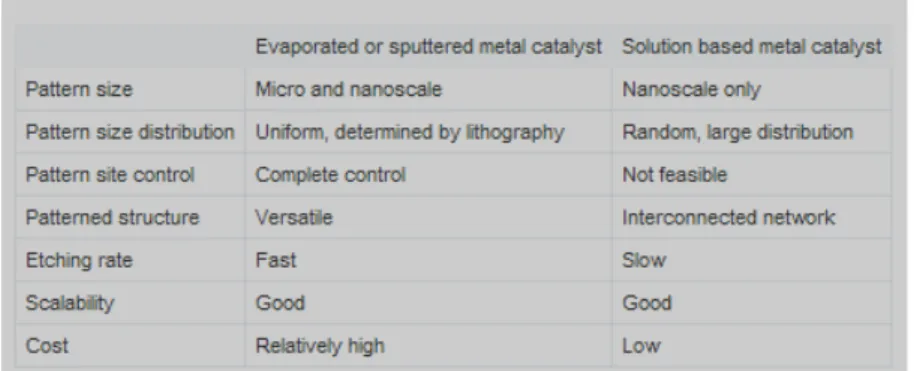
Patterned metal deposition is typically carried out with different methods, e.g., photolithography or Block Copolymer Lithography (BCP) combined with evaporation, electrodeposition or molecular beam epitaxy (MBE). Table1. 1 compares the advantages and disadvantages of the MAcE characteristic when a solid metal thin film mesh or a solution based metal is employed. The latter is simple and less expensive but there is a little control on the positioning of metal on silicon surface and also on its in plane extension. As a consequence the size and shape of the produced nanostructures are not uniform because they are strictly related to the metal clusters distribution. For example, AgNO3 solution based MAcE of Si
generates Si nanowires with diameters in the range of 20-300nm.
Table 1. 1: A comparison between solid metal thin film pattern vs. solution based metal deposition. Usually EMD is employed when there is not a requirement of
strict control over the produced feature size and shape.
In the following paragraphs an overview on the techniques employed up to now to pattern metal on silicon substrate for subsequent MAcE will be given.
1.5.1 Nanospheres lithography
31
inexpensively produce nanoparticle arrays with controlled shape, size, and interparticle spacing. It makes use of nanospheres placed in a tightly packed array on a substrate, in order to create a mask for thin film deposition or etching. By removing the spheres, the remaining 2-D array on the substrate has triangular shaped nanostructures in a hexagonal pattern, often called a Fischer pattern [52].
In the experiments of Huang et al. [53] a self assembled monolayer of polystyrene sphere (PS) array was produced on silicon (see fig. 1.21). Their size reduction was achieved by a RIE (Reactive Ion Etching) process. Subsequently, a noble metal (silver) film was deposited by thermal evaporation through the PS mask. The process resulted, after removal of PS, in a continuous layer of noble metal with an ordered array of pores, whose diameter was strictly related to that of the RIE etched spheres (according to the recently developed techniques, it could range from 200nm to several micrometers). The patterned substrate was then etched in the etching solution containing HF and H2O2 and an ordered array of
32
Fig.1. 21: (a) Scheme showing the processes in a method combining nanosphere lithography and metal-assisted chemical etching [50]: after the deposition of a nanospheres array and the diameter reduction, through a dry etching process, a
noble metal film is sputtered on the substrate. The subsequent metal assisted etching generated an ordered array of silicon nanowires. (b) SEM image of Si nanowire arrays fabricated by the method combining nanosphere lithography
and metal-assisted chemical etching.
In practice, it is difficult to assemble polymer spheres with diameters less than 200nm into a highly ordered monolayer array. In order to achieve Si nanowires with diameters less than 20nm, the mask must be obtained by reducing the diameter of spheres of much larger diameter. This process usually leads to an irregular shape of the remaining polymer and it is therefore not appropriate for the fabrication of Si Nanowires with well defined circular cross section. In addition, a limitation in the obtainable
33
metal pattern size is expected: it is difficult to successfully pattern a noble metal film with arrays of discrete holes if the typical thickness of the noble metal film is comparable to the height of the size reduced polymer mask. The nanosphere lithography method is usually limited to Si nanowires with diameter larger than 50nm.
1.5.2 AAO Mask Method
This method was proposed to overcome the limitations induced by nanosphere lithography. The masking material is the Anodic Aluminum Oxide (AAO) and is fabricated by anodization of aluminum. The process results in a thin Al2O3 foil containing pores of diameter from 10 to 350nm
with a density ranging from 5x10⁸ pores per cm2 to 3x10¹⁰ pores per cm2 [54]. The pore size and pore density of the ultrathin AAO membranes (i.e., interpore distance) could be changed by varying the electrochemical parameters (e.g., voltage and electrolyte) of the anodization reaction of aluminum.
In the technique employed by Huang et al. [55], an ultrathin AAO membrane (thickness ≈300 nm, pore diameter ≈20 nm) was placed on a Si substrate via a solution-based transfer process. RIE was then performed to transfer the AAO membrane pattern to the wafer. In fig.1.22 the Si substrate after this step, with the etched pits, is reported.]
Fig.1. 22: Etched pits on silicon substrate from the experiments of [ref] after transfer of the AAO mask with RIE. The AAO mask is partially removed to show
34
The features of the AAO membrane were transferred onto the underlying Si substrate with a high degree of fidelity. After its removal, a thin layer of noble metal was deposited onto the patterned Si. It was characterized by a continuous film with holes corresponding to those on the substrate). The side walls of the pores stayed uncovered while silver, at the bottom of each hole, exists as a discrete particle disconnected from the silver film on the surface of the silicon substrate.
By etching the metal-covered Si substrate in an etchant containing HF and H2O2, the substrate was transformed into Si nanowires (see fig. 1.23).
Fig.1. 23: Scheme showing the fabrication process of a method combining an AAO mask and metal-assisted chemical etching. (a-b-c-d) AAO membrane on silicon, dry etching for mask transfer, metal deposition and chemical etching. b) SEM of the obtained array of SiNWs and c) plan-view SEM images of vertical nanowires.
Inset in (c) shows the regular diameter distribution of theSi nanowires.
Experimentally the etching rates are different for the metal mesh and the isolated metal particles that after etching are usually located in a thin porous layer at the top of each wire. It cannot be excluded some are lost from the top of the Si nanowire by non-vertical etching.
35
1.5.3 Interference Lithography Method
Another approach is that based on Interference Lithography (IL), developed by Choi et al.[57] The Si substrate is spin coated with a thick (about 400 nm) layer of photoresist. An IL system (a Lloyd’s mirror type interference lithography setup with a 325 nm wavelength laser source) is employed for the exposure. After developing, oxygen plasma etching is employed to reduce the size of the remaining photoresist and to remove the residual unexposed photoresist. The substrate was then subjected to a metal (Au) deposition and to the assisted chemical etching, resulting in a perfectly ordered Si nanowires array (see fig. 1.24) with diameters of about 150nm. Recently the size of the obtained structures has been reduced to 60nm.
Fig.1. 24: Scheme showing the processes involved in a method combining interference lithography and metal-assisted chemical etching. The exposed photoresist is a mask for metal deposition. The corresponding SEM image of the
36
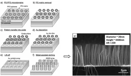
1.5.4 Block-Copolymer Mask Method
Chang et al. used block-copolymers as a mask to fabricate a metal mesh, creating high aspect ratio Si nanowires with diameters less than 20 nm. [58]. A thin layer of SiO2 was evaporated on a Si substrate (see fig. 1.22). A
diblock copolymer (polystyrene-block-ployferrocenyldimethylsilane PS-b-PFS), was then spin coated on the SiO2/Si. Vacuum annealing was
performed to achieve the micro-phase separation. The PS matrix was removed by oxygen plasma, leaving behind PFS as dot arrays on the SiO2/Si
substrate. The SiO2 film was etched into pillars by RIE with the PFS dots
acting as a mask.
Fig. 1.22 Scheme showing the processes involved in a method combining block-copolymer mask and metal-assisted chemical etching.(a) PS-PFS micromembrane and microphases separation, (b) PS matrix removal and (c) mask transfer to SiO2.
(d) Metal deposition took place on the uncovered region. (e) After liftoff an ordered metal mesh was obtained with the subsequent etching (f) nanowires
were obtained. (g) SEM image of Si nanowire array fabricated by a method combining a block-copolymer mask and metal-assisted chemical etching
37
mask. They were removed in diluted HF solution, leaving behind a mesh on the Si substrate. The diameter of the pores had a good fidelity to the diameter of the PFS dots. Finally, ordered arrays of Si nanowires were obtained by etching the Si substrate with the Au mesh in an etchant containing HF and H2O2. By this approach, diameters of the Si nanowire as
small as 19 nm could be realized. The spacing between the nanowires was 10 nm.
As shown the advantages of this fabrication technique are numerous, indeed:
• A good control of etch rates has been achieved;
• The experimental requirements are very simple, safe and low cost; • It is possible to machine large area substrates;
• it is possible to achieve long vertical etch depth starting from narrow overtures, overcoming the limits of dry etching techniques- Two drawbacks limit the large diffusion of this fabrication technique: a control of axial orientation of the etched nanostructures and an accurate and simple metal positioning on silicon surfaces.
38
CHAPTER 2
ELECTROLESS SILVER DEPOSITION ON (100) AND (111)
SILICON SUBSTRATES
In this chapter the Electroless Metal Deposition of Ag will be investigated on both (100) and (111) oriented Silicon substrates.
Wafers were processed in two distinct configurations:
a. Simple (100) and (111)Si wafers as starting substrates,
b. Macro-patterned with anisotropic etching in alkaline solution sample, that allows the simultaneous exposure of (111) and (100) contiguous surfaces to the deposition solution.
Silver atoms preferably deposit on surface discontinuities so the electroless metal nuclei density should depend on the surface unsaturated bond density of the exposed areas [59]. This factor varies with crystallographic orientation and with the morphology of the substrates.
It has been shown (chapter 1) that the deposition rate is very fast during the first few seconds and then it levels at a lower value of at least one order magnitude for the (100) oriented wafer. The same trend as it will be reported occurs also for the (111) oriented wafer and the amount of deposited silver is weakly dependent on orientation.
When deposition was performed in configuration b), an inhomogeneous silver distribution was obtained: the metal ions agglomerate preferentially on the convex interplanar transition region between the two exposed
39
surfaces, rich of kinks and nano-terraces. The metallic cluster density and size decrease with the distance from it. In addition, deposition resulted orientation dependent, being higher on the (100) surface.
2.1 Influence of substrate morphology.
According to the data reported in the literature, surface morphology has a strong influence during electroless metal deposition. Structural modified regions can catalyze metal ions deposition and clustering leading to a self selective mechanism on large area substrates.
It has been demonstrated that metal deposition occurs preferentially on defects sites (patterned by Focused Ion Beam or induced by scratching the Si surface with the tip of an Atomic Force Microscope). In the experiments of Homma et al. nanoscopic patterns were generated on H-terminated (100)Si wafers by nano-indentation technique, using a scanning probe microscope (SPM) with a diamond probe [60].
By controlling the parameters such as the indentation force, nanoscopic patterns with different degrees of defects were obtained. The scanning surface potential microscopy (SPoM) analysis showed that these sites locally possessed negative shift in potential, i.e., higher activity for the reductive deposition of metal ions, which increased with an increase in the degree of defectiveness.
In the work of Chen [61] et al. silicon (100) surfaces have been locally modified by Ar+ ion implantation (beam energy 6keV with an incidence angle of 13°, for 10h) and then immersed in an HF based solution contaminated with Cu++ concentration of 100ppb. The SEM investigations are reported in fig.2.1. The white droplets are Cu nanoparticles that preferably deposited in the damaged region. A sharp boundary separates the two regions: the damaged (covered with Cu) from the undamaged one.
40
Fig.2. 1 From Chen et al. [61] the damaged ring where it copper deposited according to a self selective mechanism.
Choi et al. [62] demonstrated that self selective electroless plating could be achieved on silicon by simply scratching the surface with an AFM tip, as reported in fig. 2.2. The copper deposition was strongly enhanced in the defective regions and increased with increasing immersion time.
Fig.2. 2 SEM micrographs by Choi et al. [62] of copper selectively deposited on scratches induced with an AFM tip. (a) Cu 5ppm, 10min; (b) Cu 5ppm, 20min; (c)
Cu 5ppm, 30min and (d) Cu 2ppm, 30min.
These experiments indicate clearly that some regions in silicon are energetically favorable for metal deposition. They correspond to those in
41
which crystal lattice is partially or totally destroyed, that is, defect sites or amorphous regions. Dangling bond density in these regions is expected to be higher than in other undamaged regions. They are more chemically active and can be oxidized more easily. Although the dangling bonds are passivated by fluorine or hydrogen in dilute HF solution, they have still a higher energy than a Si-Si bond in bulk silicon crystal.
The detailed explanation for the observed trend is hard to achieve, however the exact positioning of the metal catalyst on silicon surface is essential to obtain ordered arrays of silicon nanostructures.
2.2 Silver deposition on individual Si(100) and Si(111).
2.2.1 Experiments
The Silver Nanoparticles (AgNPs) formation and growth were investigated for both oriented Si substrate and for different time of immersion in a solution containing HF and Ag+.
Si (100) n-type (P-doped ρ ≅ 3-5Ω⋅cm) and Si (111) n-type (P-doped ρ ≅ 0.1-0.16Ω⋅cm) wafers were used as starting materials.
A thick layer of AZ resist was spun coated on the back of each wafer, to prevent silver deposition during the immersion in the solution. It has been found that this resist is a very useful masking material during MAcE [63]. The samples were cut in squares of 0.5cm in side and dipped in Diluited Hydrofluoridric Acid Solution (DHF, Hydrofluoridric Acid and Water 1:7). By this treatment, adopted to remove the native oxide, H-terminated surfaces were obtained.
The electroless silver deposition was achieved by samples immersion in solution I (0.005M AgNO3 and 4.8M HF) for times in the range 5s to 160s to
guarantee a detailed investigation on Metal Nanoparticles generation and growth.
It should be pointed that for short deposition times, e.g. 5s, one makes a lot of errors. Immersion and extraction times are significant in respect to the 5
42
second dip and also the rinsing of the reactants away from the surface is at least on the same time scale. This factor should be considered when a comparison between the (100) and (111) wafers at 5s is done. Nevertheless short times are useful to delineate a trend for nucleation and early stages of growth of silver particles.
The as-deposited samples were analyzed with various techniques: SEM, RBS and cross section TEM.
2.2.2 Results
The SEM investigations performed on the same samples are reported in fig. 2. 3.
They show that after 5s of immersion, in agreement with the data reported in chapter 1, a large amount of silver nuclei are present on both (100) and (111)Si substrates (fig. s 2.3a and 2.3e). Then, for a prolonged immersion duration, the AgNPs grow in size and interconnect in between them, covering partly the silicon surface.
43
Fig.2. 3: SEM images of (100) and (111) Si substrates after Ag plating for (a) (100) 5s; (b) (100) 40s; (c) (100) 120s; (d) (100) 160s; (e) (111) 5s; (f) (111) 40s; (g) (111)
120s; (h) (111) 160s
It is interesting to observe that even after 160s of immersion a continuous metal film is not achieved, according to the proposed 3D island growth
44 mode.
The RBS spectra of 2MeV He+ ions have been recorded for all the samples. They show that the amount of deposited Ag increases with immersion time for both oriented substrates, as reported in fig. 2.4 in terms of atomic density. The AgNPs density instead, obtained with the elaboration of SEM micrographs of fig. 2.3, is reported in fig. 2.5.
0 20 40 60 80 100 120 140 160 180 2 4 6 8 10 12 x 1016 A to m s /c m 2 Deposition Time [s] (100)Si (111)Si
Fig.2. 4 Ag (Atoms/cm2) from RBS analyses for the (100) and (111) Silicon substrates.
45 0 20 40 60 80 100 120 140 160 180 1 2 3 4 5 6 7 8 x 10¹⁰ A g N P s /c m 2 Deposition Time [s] Si(100) Si(111)
Fig.2. 5: Silver cluster density as a function of the immersed time.
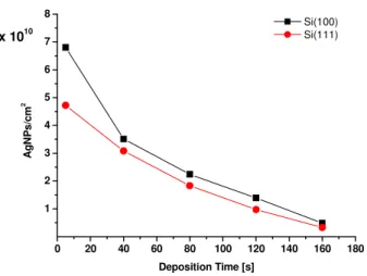
The data reported in fig. 2.4 indicate that for the two oriented substrates, within the experimental uncertainties the deposition rates coincide, even if the silver amount is slightly higher on (100)Si.
Fig. 2.5 shows a higher density of silver clusters, at all the investigated deposition times for (100)Si. The nuclei density calculated at 5s is very high, about 7x10¹⁰ AgNPs/cm2 for (100) and 5x10¹⁰ AgNPs/cm2 for (111)Si. Then the particles’ density decreases: for the (100) substrate: it is 7x10⁹ AgNPs/cm2 at 160s deposition time and for the (111) substrate is nearly half, 3x10⁹ AgNPs/cm2.
To summarize, the first few seconds of deposition are characterized by a fast rate, during which the amount of silver atoms is 1016 atoms/cm2 (fig. 2.4) with a nuclei density of 1010 cm-2 (fig. 2.5). For longer times the silver deposition rate is nearly constant for both substrates (it varies of a factor 2 form 40s to 160s as reported in the RBS spectra of fig. 2.4) while the cluster density decreases of one order magnitude due to the coalescence.
However the deposition shows a weak dependence on the substrate’s orientation.
46
clusters’ density an increasing mean extension for particles occurs. Indeed it grows of two order magnitude form 5s to 160s. Generally it is the same for both orientations except that at 160s when it is nearly a factor of two higher for the (111) oriented substrate. This is probably the effect of lower particle density on coalescence (i.e. the particles span on a larger area).
0 20 40 60 80 100 120 140 160 180 0,4 0,8 1,2 1,6 2,0 2,4 2,8 x 10⁴ C lu s te r m e a n S iz e [ n m 2] Deposition Time [s] (100)Si (111)Si
Fig.2. 6: Silver cluster mean size versus deposition time.
The density of the silver clusters is higher on (100)Si, but they are smaller than those more dense found on (111)Si. The amount of deposited silver is nearly the same for both orientations. As a result of these two different trends the covered area is nearly the same for the two substrates as shown by the data reported in fig 2. 7.
47 0 40 80 120 160 0,1 0,2 0,3 0,4 0,5 0,6 0,7 0,8 0,9 Si (100) Si (111) C o v e ra g e Deposition Time [s]
Fig.2. 7 Surface coverage of Ag clusters on (100), (111) Si substrates, for different dipping times.
In the first 5s, the covered area reaches the 40%, then the deposition rate slows down and the measured coverage doubled in 155s of immersion. Coverage as obtained by SEM images elaboration is weakly orientation dependent, just like Ag amount and the clusters density. It is clear that the adopted method to analyze the SEM images could lead to certain incertitude.
Some samples were analyzed by TEM cross section and typical images are shown in fig. 2.8 for both oriented substrates and for two different deposition times: 40s (fig. 2.8a-b) and 160s (fig. 2.8c-d) respectively.
48
Fig.2. 8: Cross section transmission microscopy images (a) (100)Si 40s, (b) (111)Si 40s for 160s; (c) (100)Si 160s; (d) (111)Si 160s oriented substrates respectively.
The silver clusters increase in size with deposition time not only laterally but also vertically, the mean height is about 22nm at 40s while it is 40nm at 160s. if we compare the thickness variation with the square root of the mean area, plotted in fig.2.6, we could observe that while the height varies of a factor two in 120s, the in plane extension changes of a factor 4, confirming that during this stage of deposition the main effect is particles coalescence. Some grain boundaries could be observed on particles thus supporting the occurrence of coalescence.
A thin oxide layer is visible at the interface Ag/Si, that it is quite rough especially for the (100) substrate. This may be due to a higher reactivity of the (100) surface as kinks and dislocations are present in larger amount. It is known indeed, that Si(100) undergone a (111) faceting in oxidative solution [64]. No intermixing of Ag with Si has been detected [65].
49
2.2.3 Considerations about the orientation dependence of Electroless Ag Deposition.
The nucleation and growth mechanism of AgNPs on silicon substrates have been exploited elsewhere [66-70]. From the measurements presented in the previous section a fast silver deposition occurs on both oriented substrates during the very first seconds (less than 5s) of immersion in the plating solution reaching a coverage of about 40%, thereafter the rate slows down of a factor ten and it remains constant and uniform for both oriented substrates. At the maximum adopted deposition time, i.e. 160s, the surface coverage reaches 70% in both substrates. This behavior implies a change in the electrical response of the silicon surface. Soon as part of the silicon is covered by silver a Schottky barrier is formed with a depletion layer of 0.12μm for the 3-5 Ω⋅cm type Si (100) and 0.09µm for the 0.1 Ω⋅cm n-type (111) Si respectively.
The depleted layer extends also laterally and as a result the Ag+ ions prefer to deposit onto the preexisting silver clusters than on the uncovered silicon surface. The data indicate moreover that the AgNPs density is higher on Si (100), but their means size is lower in comparison with Si (111). The difference might be attributed to the different reactivity of the two surfaces because of the higher number of surface bonds and of stable H-termination sites in HF treated Si (111) surfaces. In any case the incertitude in times due to the experimental conditions, does not allow a clear detection of orientation dependence for electroless silver deposition.
To elucidate if there is a dependence on the substrate orientation, deposition was performed simultaneously on (100) and (111)Si by means of the apparatus reported in fig.2.9 The deposition time was chosen long enough (30min) to overcome incertitude associated with immersion and extraction of samples.
50
Fig.2. 9:Experimental setup for simultaneous deposition of silver on Si(100) and Si(111)
In fig. 2.10 the SEM plane views of both substrates are depicted. The silicon surface of both substrates is covered with dendritic silver clusters that are more dense on (100)Si.
Fig.2. 10:. In plane SEM of(100)Si and (111)Si deposited for 30min
The higher Ag amount on (100)Si was confirmed by cross section SEM, as reported in fig. 2.11.
51
Fig.2. 11: Cross section SEM of samples after 30min deposition (a) Si(100) and b) Si(111).
The analyses confirm that deposition is orientation dependent, being faster on (100)Si. However these dendritic clusters don’t allow the fabrication of silicon nanostructures, because, as explained in the previous chapter, they originate from the empty spaces in between metal particles. Nevertheless the experiment shows that orientation dependence for silver deposition could be postulated.
In the next paragraphs, indeed, deposition will be investigated on a substrate that allows the contiguous exposure of (100) and (111) surfaces to the plating solution. In this configuration the incertitude due to the dipping and rinsing in the individual processing was eliminated and the orientation dependent behavior for silver deposition could be investigated also for shorter times.
2.3 Silver deposition on macro-patterned Si wafers: simultaneous exposure of contiguous (100) and (111) surfaces.
2.3.1 Fabrication of macro-patterned Si.
The starting substrate was n-type Si(100) (P-doped ρ = 3-5 Ω·cm) with a 300nm thick thermal SiO2 overlayer. The mask for the macro pattern was a
strip 700μm wide and millimeters long, it was obtained by contact lithography, using a UV flood lamp.
52
The {100} and {111} Si planes were obtained by means of the anisotropic etching [71] with alkaline solutions (KOH Potassium Hydroxide).
The obtained pattern depends on the mask features while its morphology is strictly related to the adopted experimental parameters, i. e. etching time and temperature.
2.3.2 A brief overview on KOH etching of Si
A schematic representation of etching in KOH solutions on masked (100)Si is reported in fig. 2.12. Etching starts with the fast, vertical removal of (100) atoms. Near the mask, the (100) planes are covered and so etching leaves the (111) atoms exposed. According to the back bond breaking theory an atom on (111) surface is harder to remove than one on (100) and etching will proceed slowly in the [111] directions. As a result the walls of the obtained holes are the four (111) planes, tilted of 54.74° respect to the horizontal direction.
![Table 2. 1: Etch rate [μm/h] for various molarities and temperatures [71]. At 20%wt and about 80°C the expected etch rate is between 50 and 86 μm/h](https://thumb-eu.123doks.com/thumbv2/123dokorg/4482579.32388/62.892.208.675.277.491/table-etch-rate-various-molarities-temperatures-expected-etch.webp)
![Table 2. 2 Surface bond density of (100) and (111) Silicon surfaces. From ref [72.]](https://thumb-eu.123doks.com/thumbv2/123dokorg/4482579.32388/63.892.232.670.153.388/table-surface-bond-density-silicon-surfaces-ref.webp)
