square nanorings fabricated by
focused electron beam induced deposition
Federico Venturi*1,2, Gian Carlo Gazzadi2, Amir H. Tavabi3, Alberto Rota4,
Rafal E. Dunin-Borkowski3 and Stefano Frabboni1,2
Full Research Paper
Open AccessAddress:
1FIM Department, University of Modena and Reggio Emilia, Via G. Campi 213/a, Modena I-41125, Italy, 2CNR – Nanoscience Institute, S3 Center, Via G. Campi 213/a, Modena I-41125, Italy, 3Ernst Ruska-Centre for Microscopy and Spectroscopy with Electrons and Peter Grünberg Institute, Forschungszentrum Jülich, 52425 Jülich, Germany and 4Intermech-Mo.Re. Center, University of Modena and Reggio Emilia, Via Vignolese 905/b, Modena I-41125, Italy
Email:
Federico Venturi* - [email protected]
* Corresponding author
Keywords:
focused electron beam induced deposition; magnetic force microscopy; magnetic nanostructures; off-axis electron holography; transmission electron microscopy
Beilstein J. Nanotechnol. 2018, 9, 1040–1049.
doi:10.3762/bjnano.9.97
Received: 30 November 2017 Accepted: 28 February 2018 Published: 03 April 2018
Associate Editor: J. J. Schneider
© 2018 Venturi et al.; licensee Beilstein-Institut. License and terms: see end of document.
Abstract
The magnetic properties of nanowires (NWs) and square nanorings, which were deposited by focused electron beam induced depo-sition (FEBID) of a Co carbonyl precursor, are studied using off-axis electron holography (EH), Lorentz transmission electron microscopy (L-TEM) and magnetic force microscopy (MFM). EH shows that NWs deposited using beam energies of 5 and 15 keV have the characteristics of magnetic dipoles, with larger magnetic moments observed for NWs deposited at lower energy. L-TEM is used to image magnetic domain walls in NWs and nanorings and their motion as a function of applied magnetic field. The NWs are found to have almost square hysteresis loops, with coercivities of ca. 10 mT. The nanorings show two different magnetization states: for low values of the applied in-plane field (0.02 T) a horseshoe state is observed using L-TEM, while for higher values of the applied in-plane field (0.3 T) an onion state is observed at remanence using L-TEM and MFM. Our results confirm the suit-ability of FEBID for nanofabrication of magnetic structures and demonstrate the versatility of TEM techniques for the study and manipulation of magnetic domain walls in nanostructures.
Introduction
Magnetic nanostructures are studied intensively for their applications in high-density data storage [1,2], magnetic random access memory [3], magnetic logic nanodevices [4]
and magnetic sensing [5]. A new concept of fast memory, which is referred to as racetrack memory, has been proposed, based on the motion of domain walls along a nanowire (NW)
subject to current pulses or external magnetic fields [6]. The strong research interest in such new types of memories is based on their promise for reliable, high-capacity and high-perfor-mance devices [7]. However, in all of the proposed applications, the stability of the magnetic state of the nanostructure depends on factors such as its composition, crystal structure and shape [8].
Co-based magnetic nanostructures can be deposited by focused electron beam induced deposition (FEBID) of Co carbonyl (Co2(CO)8). This is a direct-write technique performed in a scanning electron microscope (SEM) equipped with a gas injector system (GIS) [9]. It exploits secondary electron emis-sion resulting from interaction of the primary electron beam with a substrate to decompose molecules that are adsorbed on the surface. The non-volatile part of the molecule is deposited, whereas volatile ligands are pumped away. FEBID is a versa-tile technique for nanoprototyping and research, as it permits the deposition of material in a variety of shapes with high spatial resolution. Moreover, it is also possible to deposit oxides [10] and, by co-injecting different precursors, alloy materials with tunable properties [11]. A review of the application of the technique to the deposition of magnetic nanostructures has recently been published [12]. It should be noted that Co carbon-yl precursor was chosen here because it has been shown to provide high purity deposits with magnetic properties that are close to those of pure Co [13].
It is well known that shape anisotropy has a profound influence on the magnetic properties of nanostructured materials. The NW is a basic building block of magnetic nanodevices, as its high aspect ratio (length/width) often results in a single magnet-ic domain state due to shape anisotropy [14]. In detail, a NW has a stable magnetic state if its width is smaller than 7·Δd, where Δd is the dipolar exchange length [15], which is ca. 3.4 nm for Co [16]. Ring shapes have also been proposed as ele-ments for magnetic memories thanks to their higher stability compared to filled shapes [17]. Square nanorings, in particular, are attractive since their right-angle vertices provide well-defined reference points for magnetization orientation, while magnetostatic interactions between different sides give rise to different possible magnetization states [18]. Extensive work has previously been performed on Co nanostructures using magnet-ic force mmagnet-icroscopy (MFM) [19,20], Lorentz-transmission elec-tron microscopy (L-TEM) [21] and elecelec-tron holography (EH) [22].
Here, we use different techniques and different magnetization conditions to investigate the magnetic states of NWs and square nanorings formed from four NWs. The magnetization states of the square nanorings are studied both in the presence of an
applied magnetic field and at remanence, revealing different magnetization states and allowing for step-by-step imaging of magnetization reversal processes.
Experimental
FEBID was performed in a dual-beam system (FEI Strata DB 235M) using the following electron beam parameters: 1 μs dwell time, 90% overlap and 85 and 130 pA beam currents for energies of 5 and 15 keV, respectively. The base pressure in the chamber was 2.2 × 10⁻⁶ mbar, whereas during deposition it was 3.3 × 10⁻⁶ mbar. NWs that had lengths of 2.5–3.0 µm, widths of 70–100 nm and thicknesses in the range of 10–40 nm were deposited directly on C TEM grids. Square rings were formed from 4 NWs of length 1 µm, width 100 nm and nominal thick-ness 40 nm and were deposited onto both C grids and Si sub-strates. Their shape was designed using the built-in pattern generator and comprised four rectangles with partially overlap-ping sides, scanned in parallel. The refresh time between subse-quent passes was negligible. This fabrication approach could lead to local small thickness inhomogeneities in areas where the rectangles overlap. The amorphous C and Si substrates were used for TEM and MFM studies, respectively. All depositions and analyses were carried out at room temperature. Although most of the deposited material consisted of Co, some C and O were present in the fabricated structures due to incomplete dissociation of the precursor molecules. In particular, a more significant halo of deposited material was observed near the structures grown on Si. This was caused by larger secondary electron generation by the primary beam interacting with the Si substrate, which is thicker and denser than the C substrate. Energy-dispersive X-ray spectroscopy (EDX) provided measured compositions that depended on the substrate and deposition energy. A spectrum recorded from the bare substrate was subtracted from the sample spectrum in order to remove the substrate contribution. Each concentration measurement was affected by a 5% uncertainty. After subtraction, the overall uncertainty is estimated (from the squared sum of uncertainties of the two spectra) to be 7%. For the samples on C grids, the measured Co concentration was up to (69 ± 5) atom % for 5 keV deposition and (61 ± 4) atom % for 15 keV deposition. For deposition on Si at 5 keV, the Co concentration was measured to be up to (74 ± 4) atom %. Structural information about the NWs was known from a previous study [23]. Briefly, they consist of nanocrystalline Co grains embedded in a carbo-naceous matrix. Selected area electron diffraction shows a mix-ture of hexagonal close-packed (HCP) and face-centered cubic (FCC) Co crystal structures [23].
Magnetic characterization in the TEM was carried out using off-axis EH and L-TEM in Fresnel mode [24]. We used a JEOL JEM-2010 TEM operated at 200 kV for L-TEM and an FEI
Titan TEM operated at 300 kV for off-axis electron holography. L-TEM is an imaging technique that enhances local phase gradients, such as those associated with the presence of magnet-ic domain walls [25,26]. Fresnel images were taken underfocus in low magnification mode, using the objective mini-lens as the imaging lens, with the objective lens slightly excited (at 10% of the value used for eucentric focus), in order to impart a speci-men-tilt-angle-dependent magnetic field to the sample. Off-axis electron holography [27] is an interferometric technique that allows the retrieval of real-space phase images of samples in the TEM [28], from which information about the projected electro-static potential and in-plane magnetic field within and around the specimen can be determined. In the present study, a voltage of 53 V was applied to an electron biprism when recording off-axis electron holograms. Measurements involved acquiring an electron hologram of the sample, a vacuum reference electron hologram and then repeating the measurements with the sample turned over. Reconstruction of the electron holograms was per-formed using the software Holoworks [29]. The reconstructed phase images were aligned with each other digitally and half of the difference between them was evaluated to subtract the mean inner potential contribution to the phase, in order to obtain the magnetic contribution to the phase alone [30], both outside and inside the sample. MFM is a microscopy technique that is closely related to atomic force microscopy (AFM) [31]. The scanning tip is magnetized and is therefore sensitive to magnet-ic fields generated by the sample. Attractive and repulsive forces between the tip and the sample are measured and a two-dimensional magnetization map can be recorded. MFM analy-sis was performed with a VEECO EnviroScope system, working in tapping mode with amplitude detection feedback. The MFM maps were acquired in two-pass lift-mode, with the magnetic signal collected about 30 nm above the surface. The probe used was a Veeco MESP probe, which was made from Sb-doped (n) Si covered by CoCr. The tip was magnetized out-of-plane in a 0.32 T field.
Results and Discussion
Electron holography of nanowires
A first magnetic analysis was carried out on the NWs using off-axis electron holography. The measurements were performed on as-deposited samples without applying an external magnetic field. Two different sets of NWs on amorphous C substrates were studied: one deposited at a beam energy of 15 keV and another deposited at a beam energy of 5 keV. In each sample, the deposited shape was the same: 2.5 µm in length, 50 nm in width and with deposition times that varied between 10 and 60 s in 10 s steps. For each deposition time, the deposited thickness was found to be similar in each set, as revealed by energy-filtered TEM (EFTEM) thickness maps [32]. The material deposited at 5 keV had a width that was much larger than that at
15 keV. Figure 1a shows the cosine of 18 times the magnetic contribution to the phase recorded using off-axis electron holog-raphy from the different NWs.
The strength of the magnetic signal from each NW can be measured semi-quantitatively by counting the number of black contours across it. The magnetic signal can be seen to increase with deposition time, as more material generates a greater netic signal. However, 5 keV deposition results in a higher mag-netic phase shift than 15 keV deposition for the same deposi-tion time. The magnetic phase contours suggest visually that the NWs form monodomain states, with their magnetization aligned along their long axes due to shape anisotropy [13]. Impurities are present on some samples (especially for the 20 s and 40 s depositions at 5 keV), resulting in flux-closure domain states, which deform the dipole-like phase structure locally. These impurities are unfortunately an unavoidable by-product of our deposition process, since the electron column is not equipped with fast blanking plates and the beam tends to rest in some po-sition for a while before being blanked.
The step in the magnetic contribution to the phase Δφmax across each NW at the mid-point along its length (i.e., where it is maximum), which is approximately proportional to its magneti-zation multiplied by the cross-sectional area of the magnetic material within it, is shown in Figure 1b. It increases with depo-sition time and is greatest for 60 s at 5 keV, where it reaches a value of 4.3 rad.
The measurements confirm that deposition at 5 keV results in a stronger magnetic signal than deposition at 15 keV. This differ-ence results in part from the 5–10% higher relative content of Co for the 5 keV depositions, which was revealed using EDX analysis and is consistent with literature data [33,34]. The slightly higher Co content for depositions at lower energy can be interpreted as a thermal effect resulting from power dissipa-tion of the primary beam closer to the surface [35]. Further-more, the 5 keV depositions are wider than the 15 keV deposi-tions, resulting in a larger amount of magnetic flux across the corresponding NWs.
Based on the electron holographic measurements, it is possible to estimate the in-plane component of magnetic induction in the sample [36]. For a uniformly magnetized NW,
, where is the magnetic flux quantum and Σ is the cross-sectional area of the NW. The present NWs are not exactly cylinders: their cross-sectional areas are larger at their bases and their cross-sectional shapes are more Gaussian-like, with some lateral broadening for depo-sitions at 5 keV. Nevertheless, an approximate calculation can be carried out by using the actual cross-sectional areas
Figure 1: (a) Cosine of 18 times the magnetic phase shift recorded using EH from Co NWs deposited at electron beam energies of 15 and 5 keV for increasing deposition times (from 10 to 60 s). The black equiphase contours have a dipolar form, in particular for longer deposition times and for deposition at 5 keV, leaving one vertex of each NW and entering the opposite one. (b) Steps in phase Δφ across the NWs, measured at their mid-points, as a function of deposition time. 5 keV deposition results in larger values of Δφ than 15 keV deposition. (c) Magnetic induction values of the NWs calculated from Δφ, showing saturation for longer deposition times and higher values for the lower deposition energy.
measured from EFTEM thickness maps. The measured magnet-ic induction as a function of the deposition time is shown in Figure 1c. For the same deposition time, is higher for depo-sitions at 5 keV. There is also an increasing trend with increas-ing deposition time, which tends to saturate at 50–60 s.
For the 5 keV samples, values of up to (1.3 ± 0.2) T are reached for the highest deposition time (60 s). This value is apparently higher than that reported recently [37] for vertical nanopillars with the same Co purity. The discrepancy could be explained by the growth geometry of the deposit, i.e.,
on-sub-strate vs vertical. A vertical structure has roughly twice the sur-face area exposed to oxidation with respect to an on-substrate-grown structure, and the same authors have shown that surface oxidation is responsible for a decrease in magnetic induction by up to 30% in Co nanopillars [38]. Following this argument, the B value measured in our nanowires should be 15% higher than that for vertical nanopillars with the same Co purity. This turns out to be in perfect agreement with our recent work [39], where a B value of 1.1 T was measured for vertical Co nanopillars having the same composition, within experimental error, as the nanowires presented here. Taken together, these results indicate that on-substrate deposition at lower energy is more suitable for obtaining highly magnetic NWs. The following analyses are therefore presented only for deposition at 5 keV.
Lorentz TEM of nanowires
Further investigations of the magnetic properties of the NWs and nanorings were carried out using L-TEM. The microscope objective lens was used to apply a vertical magnetic field to the sample, which was tilted to introduce a component of the lens field in the sample plane. The pre-calibrated value of the applied vertical magnetic field B was 0.6 T [40]. For a tilt angle θ, the in-plane magnetic field applied to the sample was Beff = B·sin θ. The angle was varied over a 3.0° range in steps of 0.1°, corresponding to a maximum value for Beff of 2 × 10⁻² T. This value was chosen because, for weak applied magnetic fields, the sample is not at saturation and different magnetic domain configurations can be studied.
A representative image of a NW is shown in Figure 2a for depo-sition at a beam energy of 5 keV on a 3 × 0.05 µm2 area for 60 s, resulting in a length of 3 µm and a width of ca. 100 nm. When observed out of focus using L-TEM, the bright and dark fringes along its sides exhibit an asymmetry that is related directly to its local magnetization direction. When two magnet-ic domains with opposite directions are present in the same NW, the fringe contrast changes at a domain wall in a manner that can be described as a “kink” [41]. In Figure 2b, the Fresnel fringes have uniform contrast along almost the whole length of the NW, except for a kink at the right end, indicating that the NW has a uniform magnetic domain M1 and a smaller opposite magnetic domain M2. As the sample tilt is increased (Figure 2c), corresponding to an increasing external field Beff, the domain M2 increases in length at the expense of domain M1 and the kink shifts leftwards. This shift is slow for a wide angular range, until at a value of θ of approximately −1.0° the kink abruptly moves to the left and domain M2 extends over almost the whole length of the NW, as shown in Figure 2d. As all of the images were acquired with the B field applied, this can be regarded as a dynamic process. However, the temporal reso-lution is limited by the tilt steps and the camera acquisition
time. All of the domain shifting and reversal processes occur within this limited timescale. Therefore, time-resolved imaging of magnetization switching is unfortunately not possible. An interesting analysis can be carried out by plotting the ratio of the length of the M1 domain to the length of the NW as a function of Beff, as shown in Figure 2e. A value of 1 or 0 for the ratio corresponds to the NW adopting single-domain states M1 or M2, respectively. Magnetization saturation (Ms) is then reached and no kink is present. In the plot of the experimental data points shown in Figure 2e, the letters b, c and d corre-spond to the images shown in Figure 2b, Figure 2c and Figure 2d, respectively. The square shape of the loop is a sign of the single domain character that results from the high aspect ratio and shape anisotropy of the NW. A coercive field of approximately 10 mT is measured from the loop and is consis-tent with previous measurements on Co NWs [42]. High coer-civity is an important property in applications, as it ensures a stable magnetic state in such a nanostructure. The NWs presented here have a small enough diameter to behave in a single-domain-like manner. Higher coercivities could be achieved by depositing NWs with smaller widths.
Lorentz TEM and MFM of square nanorings
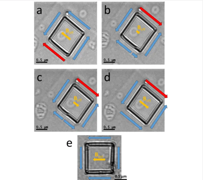
Two square nanorings, each composed of four NWs, were deposited on amorphous C and studied using L-TEM. The first nanoring was deposited at 5 keV. Each NW was deposited by scanning the beam for 50 s on a 1 × 0.05 μm2 area, resulting in sides that are 1 μm long and ca. 100 nm wide. When observed out of focus, as shown in Figure 3a, a value for Beff of 4 × 10⁻² T oriented nearly parallel to one side results in a mag-netic domain structure that is referred to as a “horseshoe” state [43]. This arrangement consists of three consecutive domains that make a “horseshoe” shape and a fourth domain, at the bottom left, which is aligned in the opposite way, in response to the direction of the applied magnetic field. In the following, the ability of L-TEM to provide a direct visualization of the switching process of the horseshoe state in a square nanoring is demonstrated. Just as for nanowires, the tilt angle was varied and the square nanoring imaged with various Beff values applied during the process. When Beff is reversed and then gradually in-creased up to a value of −0.6 × 10⁻² T (Figure 3b), the two domains that are perpendicular to the direction of the applied field are not affected. In contrast, the upper right domain reverses immediately, aligning with the field, while the lower left domain undergoes a gradual transition, supporting two opposing domains that are revealed by the presence of a kink. As the field is increased to a value of −1.7 × 10⁻² T (Figure 3c), the domain wall moves in order to increase the fraction of the NW that is aligned with the field. When the sample is brought towards saturation (Figure 3d), the kink vanishes and a
horse-Figure 2: (a) In-focus bright-field TEM image of a Co NW. (b) L-TEM underfocus image of the NW, exhibiting a kink at the right end due to a magnet-ic domain wall. The kink moves leftwards along the NW in (c) and (d) as the specimen tilt angle is increased, thus increasing the leftward-oriented component of the lens field in the sample plane (Beff). Blue and red arrows mark the opposite magnetic domains M1 and M2, respectively. (e) Hysteresis loop of the NW measured as a function of the in-plane lens field. The normalized magnetization M/Ms was determined by dividing the blue magnetic domain (M1) length by the total NW length. A saturated NW would have M1/Ms = 0, 1. The letters indicate the points corresponding to panels b–d.
shoe state appears again, but with a 180° rotation that brings the domain that is in the opposite direction to the consecutive domains to the upper right. The reversal of upper-right and lower-left sides at different field values is a consequence of their non-identical size, as shown by the micromagnetic calcula-tions in [18]. The circular dot outside the square, near the top corner, is unfortunately one of the unavoidable by-products of our deposition process. This feature does not influence the overall magnetic arrangement of the square.
A second nanoring was deposited with the same parameters, with the aim of studying its remanent magnetization state after the application of higher fields. In the TEM, in fact, the narrow tilting angle range limits the effective field values. For this reason, a nanoring was magnetized outside the microscope using an electromagnet, and applying a field Bext of 0.3 T along its side. The resulting L-TEM image, which is shown in Figure 3e, reveals a magnetization state that is different from all those previously observed, and is characterized by two pairs of
Figure 3: L-TEM images of square rings, showing the magnetization directions under different magnetic fields Beff and at remanence after applying an external magnetic field Bext. The series starts from a saturated horseshoe state in (a). When the external field is reversed, a mixed state is visible, with the lower-left side exhibiting a kink generated by a domain wall (b). As the external field is increased, the domain wall shifts in the direction oppo-site to the field (c). When Beff is increased to its maximum value, the kink vanishes and the horseshoe state appears again with a 180° rotation (d). (e) L-TEM image obtained after applying a higher magnetic field (0.3 T) along the side, before the insertion of the sample. The magnetization state is then observed at remanence, and reveals an onion state.
consecutive domains running along the sides of the square symmetrically with respect to the diagonal. Such a magnetiza-tion arrangement is referred to as an “onion” state [43]. By carrying out a quantitative analysis on Figure 3e, a contrast difference of 7–15% is revealed between the inner and outer fringes on each side of the square, which permits to assign a leftward domain orientation of the top and bottom sides and a downward orientation of the left and right sides. In the lower part of the right side a small dot corresponds to an imperfection caused by the limitations of our scanning setup. This flaw is similar to the one previously mentioned, and can be regarded as a small magnetic nanopillar causing a local magnetization
rear-rangement along the side [44]. This, however, does not seem to perturb the overall magnetic onion state, which is confirmed also by the analyses presented in the next paragraph. Horseshoe and onion states have been observed during the switching of square permalloy rings, when slight ring asym-metry [43] or slight misalignment of the external field from the square side [17] are present. By decreasing the external field from saturation, when all four domains are aligned with the direction of the applied field, an onion state is first observed, followed by a horseshoe state at a lower field. The present L-TEM results are consistent with this behavior, as the external
Figure 4: (a) AFM image of a square ring. (b) Height profile corresponding to the red dashed line in (a). (c) 3D AFM topographic map of the area in (a). (d, e) MFM images of the square ring after applying a 0.3 T external field oriented along the side (d) towards the left and (e) towards the right. Dark (bright) areas are representative of attractive (repulsive) magnetic forces between the tip and the sample. This domain arrangement, with bright and dark spots at the vertices of the diagonal, provides evidence for a magnetic onion state, as indicated by the white arrows.
field applied in the case of the onion state is higher than that applied during horseshoe state observation.
In order to validate the L-TEM results obtained at remanence and to measure the three-dimensional (3D) topography of the sample, additional analyses were carried out using AFM and MFM. A square nanoring was deposited at 5 keV on a Si sub-strate for MFM analysis. An AFM topography image is shown in Figure 4a, while a height profile taken across the middle of the nanoring is shown in Figure 4b.
Both sides have a thickness of ca. 40 nm, a length of 1 μm and a width of ca. 100 nm. A topographic map of the same area is shown in Figure 4c. In this map, a slight accumulation of deposit at the corner is visible. However, it does not appear to affect the overall magnetic state. Before performing MFM, the same external magnetic field Bext of 0.3 T, aligned with one of the sides, was applied outside the microscope. After the first analysis, it was then applied in the opposite direction. As shown in Figure 4d and Figure 4e, the remanent magnetization is aligned with a diagonal of the square and reverses along the
same diagonal after applying an opposite external field. The magnetic signal is visible in the form of bright and dark spots at opposite corners of the square, which correspond to repulsive and attractive forces on the tip, respectively. This is another manifestation of an onion state, in agreement with what previ-ously observed using L-TEM. The presence of halo deposition near the square ring contributes to the MFM signal from its surroundings. However, due to the low Co deposit amount in this halo, it does not affect the overall magnetization state of the nanostructure. The halo may at most slightly modify the coer-civity of the nanostructures [45].
Conclusion
Co NWs and square nanorings were deposited using FEBID from a Co carbonyl (Co2(CO)8) precursor and characterized magnetically using both TEM and MFM. EH measurements on as-deposited NWs revealed single-magnetic-domain states, with a higher magnetic signal for 5 keV deposition than for 15 keV deposition. This difference is thought to result from both a greater relative Co content (by 5–10% for the 5 keV deposition than for the 15 keV deposition) and a difference in NW width. L-TEM analysis of both the NWs and the square rings provided insight into the effect on magnetic domain structure of a weak external magnetic field. L-TEM images of NWs were used to reveal the presence of a square hysteresis loop with a coercive field of approximately 10 mT. L-TEM images of square nanor-ings revealed a horseshoe magnetic state, which could be changed to an opposite horseshoe state by reversing the magnet-ic field applied in situ. By increasing the external magnetmagnet-ic field and observing the nanorings at remanence, L-TEM and MFM analyses revealed the formation of a magnetic onion state. Our results confirm that FEBID is a suitable technique for depositing magnetic nanostructures with tailored geometries and that EH, L-TEM and MFM provide comple-mentary information about their static and dynamic magnetic properties.
Acknowledgements
This work was conducted within the framework of the COST Action CM1301 (CELINA). The research leading to these results has received funding from the European Research Council under the European Union's Seventh Framework Programme (FP7/2007-2013)/ ERC grant agreement number 320832. The authors would like to thank Prof. Giulio Pozzi for fruitful discussions. F.V. is grateful to Patrick Diehle for help with holographic reconstruction.
ORCID
®
iDs
Federico Venturi - https://orcid.org/0000-0002-3156-4736 Alberto Rota - https://orcid.org/0000-0002-8219-1351
Rafal E. Dunin-Borkowski - https://orcid.org/0000-0001-8082-0647
References
1. Chou, S. Y.; Wei, M. S.; Krauss, P. R.; Fischer, P. B. J. Appl. Phys. 1994, 76, 6673. doi:10.1063/1.358164
2. Chappert, C.; Fert, A.; Van Dau, F. N. Nat. Mater. 2007, 6, 813–823. doi:10.1038/nmat2024
3. Daughton, J. M. Thin Solid Films 1992, 216, 162–168. doi:10.1016/0040-6090(92)90888-I
4. Gavagnin, M.; Wanzenboeck, H. D.; Belic, D.; Bertagnolli, E.
ACS Nano 2013, 7, 777–784. doi:10.1021/nn305079a
5. Gabureac, M.; Bernau, L.; Utke, I.; Boero, G. Nanotechnology 2010,
21, 115503. doi:10.1088/0957-4484/21/11/115503
6. Parkin, S. S. P.; Hayashi, M.; Thomas, L. Science 2008, 320, 190–194. doi:10.1126/science.1145799
7. Parkin, S. S. P.; Yang, S.-H. Nat. Nanotechnol. 2015, 10, 195–198. doi:10.1038/nnano.2015.41
8. Chikazumi, S. Physics of Ferromagnetism, 2nd ed.; Oxford University Press: New York, NY, USA, 1997.
9. Utke, I.; Moshkalev, S.; Russell, P. Nanofabrication Using Focused Ion
and Electron Beams: Principles and Applications; Oxford University
Press: New York, NY, USA, 2012.
10. Schirmer, M.; Walz, M.-M.; Vollnhals, F.; Lukasczyk, T.; Sandmann, A.; Chen, C.; Steinrück, H.-P.; Marbach, H. Nanotechnology 2011, 22, 085301. doi:10.1088/0957-4484/22/8/085301
11. Winhold, M.; Schwalb, C. H.; Porrati, F.; Sachser, R.; Frangakis, A. S.; Kämpken, B.; Terfort, A.; Auner, N.; Huth, M. ACS Nano 2011, 5, 9675–9681. doi:10.1021/nn203134a
12. De Teresa, J. M.; Fernández-Pacheco, A.; Córdoba, R.;
Serrano-Ramón, L.; Sangiao, S.; Ibarra, M. R. J. Phys. D: Appl. Phys. 2016, 49, 243003. doi:10.1088/0022-3727/49/24/243003
13. Fernandez-Pacheco, A.; De Teresa, J. M.; Córdoba, R.; Ibarra, M. R.
J. Phys. D: Appl. Phys. 2009, 42, 055005.
doi:10.1088/0022-3727/42/5/055005
14. Cullity, B. D.; Graham, C. D. Introduction to magnetic materials, 2nd ed.; Wiley: Hoboken, NJ, USA, 2009. doi:10.1002/9780470386323 15. Jamet, S.; Rougemaille, N.; Toussaint, J. C.; Fruchart, O.
Head-to-head domain walls in one-dimensional nanostructures: An extended phase diagram ranging from strips to cylindrical wires. In
Magnetic Nano- and Microwires - Design, Synthesis, Properties and Applications; Vazquez, M., Ed.; Woodhead: Cambridge, UK, 2015;
pp 783–811. doi:10.1016/B978-0-08-100164-6.00025-4 16. Grujicic, D.; Pesic, B. J. Magn. Magn. Mater. 2005, 285, 303–313.
doi:10.1016/j.jmmm.2004.08.003
17. Zhu, J.-G.; Zheng, Y.; Prinz, G. A. J. Appl. Phys. 2000, 87, 6668. doi:10.1063/1.372805
18. Porro, J. M.; Berger, A.; Grimsditch, M.; Metlushko, V.; Ilic, B.; Vavassori, P. J. Appl. Phys. 2012, 111, No. 07B913. doi:10.1063/1.3677269
19. Jaafar, M.; Iglesias-Freire, O.; Serrano-Ramon, L.; Ibarra, M. R.; De Teresa, J. M.; Asenjo, A. Beilstein J. Nanotechnol. 2011, 2, 552–560. doi:10.3762/bjnano.2.59
20. Jaafar, M.; Serrano-Ramón, L.; Iglesias-Freire, O.;
Fernández-Pacheco, A.; Ibarra, M. R.; De Teresa, J. M.; Asenjo, A.
Nanoscale Res. Lett. 2011, 6, 407. doi:10.1186/1556-276X-6-407
21. Rodríguez, L. A.; Magén, C.; Snoeck, E.; Serrano-Ramón, L.; Gatel, C.; Córdoba, R.; Martínez-Vecino, E.; Torres, L.;
De Teresa, J. M.; Ibarra, M. R. Appl. Phys. Lett. 2013, 102, 022418. doi:10.1063/1.4776709
22. Rodríguez, L. A.; Magén, C.; Snoeck, E.; Gatel, C.; Marín, L.; Serrano-Ramón, L.; Prieto, J. L.; Muñoz, M.; Algarabel, P. A.; Morellon, L.; De Teresa, J. M.; Ibarra, M. R. Ultramicroscopy 2013,
134, 144–154. doi:10.1016/j.ultramic.2013.06.003
23. Gazzadi, G. C.; Frabboni, S. Beilstein J. Nanotechnol. 2015, 6, 1298–1305. doi:10.3762/bjnano.6.134
24. Chapman, J. N.; Waddell, E. M.; Batson, P. E.; Ferrier, R. P.
Ultramicroscopy 1979, 4, 283–292.
doi:10.1016/S0304-3991(79)80038-8
25. Wade, R. H. Some aspects of Lorentz microscopy. In Electron
Microscopy in Materials Science; Valdré, U., Ed.; Academic Press:
New York, NY, USA, 1971; pp 681–711. doi:10.1016/B978-0-12-780584-9.50024-6
26. Fuller, H. W.; Hale, M. E. J. Appl. Phys. 1960, 31, 238. doi:10.1063/1.1735552
27. Gabor, D. Nature 1948, 161, 777–778. doi:10.1038/161777a0 28. Pozzi, G. Electron holography of long-range electromagnetic fields: A
tutorial. In Advances in Imaging and Electron Physics; Hawkes, P., Ed.; Academic Press: San Diego, California, 2002; Vol. 123, pp 207–223. doi:10.1016/S1076-5670(02)80064-7
29. Völkl, E.; Allard, L. F.; Frost, B. J. Microsc. 1995, 180, 39–50. doi:10.1111/j.1365-2818.1995.tb03655.x
30. Tonomura, A.; Matsuda, T.; Endo, J.; Arii, T.; Mihama, K. Phys. Rev. B 1986, 34, 3397. doi:10.1103/PhysRevB.34.3397
31. Mironov, V. L. Fundamentals of Scanning Probe Microscopy; NT-MDT, 2004.
32. Egerton, R. F. Electron Energy-Loss Spectroscopy in the Electron
Microscope, 3rd ed.; Springer: New York, NY, USA, 2011.
doi:10.1007/978-1-4419-9583-4
33. Belova, L. M.; Dahlberg, E. D.; Riazanova, A.; Mulders, J. J. L.; Christophersen, C.; Eckert, J. Nanotechnology 2011, 22, 145305. doi:10.1088/0957-4484/22/14/145305
34. Córdoba, R.; Sesé, J.; De Teresa, J. M.; Ibarra, M. R.
Microelectron. Eng. 2010, 87, 1550–1553.
doi:10.1016/j.mee.2009.11.027
35. Van Dorp, W. F.; Hagen, C. W. J. Appl. Phys. 2008, 104, 081301. doi:10.1063/1.2977587
36. Dunin-Borkowski, R. E.; Kasama, T.; Wei, A.; Tripp, S. L.; Hytch, M. J.; Snoeck, E.; Harrison, R. J.; Putnis, A. Microsc. Res. Tech. 2004, 64, 390–402. doi:10.1002/jemt.20098
37. Pablo-Navarro, J.; Sanz-Hernández, D.; Magén, C.;
Fernández-Pacheco, A.; de Teresa, J. M. J. Phys. D: Appl. Phys. 2017,
50, No. 18LT01. doi:10.1088/1361-6463/aa63b4
38. Pablo-Navarro, J.; Magén, C.; de Teresa, J. M. Nanotechnology 2016,
27, 285302. doi:10.1088/0957-4484/27/28/285302
39. Grillo, V.; Harvey, T. R.; Venturi, F.; Pierce, J. S.; Balboni, R.; Bouchard, F.; Gazzadi, G. C.; Frabboni, S.; Tavabi, A. H.; Li, Z.-A.; Dunin-Borkowski, R. E.; Boyd, R. W.; McMorran, B. J.; Karimi, E.
Nat. Commun. 2017, 8, 689. doi:10.1038/s41467-017-00829-5
40. Volkov, V. V.; Crew, D. C.; Zhu, Y.; Lewis, L. H. Rev. Sci. Instrum. 2002, 73, 2298. doi:10.1063/1.1472465
41. Lohe, M. A. Phys. Rev. D 1979, 20, 3120–3130. doi:10.1103/PhysRevD.20.3120
42. Nikulina, E.; Idigoras, O.; Vavassori, P.; Chuvilin, A.; Berger, A.
Appl. Phys. Lett. 2012, 100, 142401. doi:10.1063/1.3701153
43. Vavassori, P.; Grimsditch, M.; Novosad, V.; Metlushko, V.; Ilic, B.
Phys. Rev. B 2003, 67, 134429. doi:10.1103/PhysRevB.67.134429
44. Franken, J. H.; van der Heijden, M. A. J.; Ellis, T. H.; Lavrijsen, R.; Daniels, C.; McGrouther, D.; Swagten, H. J. M.; Koopmans, B.
Adv. Funct. Mater. 2014, 24, 3508–3514. doi:10.1002/adfm.201303540
45. Fernandez-Pacheco, A.; De Teresa, J. M.; Szkudlarek, A.; Córdoba, R.; Ibarra, M. R.; Petit, D.; O’Brien, L.; Zeng, H. T.; Lewis, E. R.; Read, D. E.; Cowburn, R. P. Nanotechnology 2009, 20, 475704. doi:10.1088/0957-4484/20/47/475704
License and Terms
This is an Open Access article under the terms of the Creative Commons Attribution License
(http://creativecommons.org/licenses/by/4.0), which permits unrestricted use, distribution, and reproduction in any medium, provided the original work is properly cited. The license is subject to the Beilstein Journal of
Nanotechnology terms and conditions: (https://www.beilstein-journals.org/bjnano)
The definitive version of this article is the electronic one which can be found at: