Francesca Cucchi
VARIABILITY-AWARE DESIGN OF CMOS
NANOPOWER REFERENCE CIRCUITS
Anno 2013
UNIVERSITÀ DI PISA
Scuola di Dottorato in Ingegneria “Leonardo da Vinci”
Corso di Dottorato di Ricerca in
INGEGNERIA DELL'INFORMAZIONE
(SSD: Ing-Inf-01)
Tesi di Dottorato di Ricerca
1
Autore:
Francesca Cucchi
Firma__________
Relatori:
Prof. Giuseppe Iannaccone Firma__________ Prof. Paolo Bruschi Firma__________ Prof. Stefano Di Pascoli Firma__________
VARIABILITY-AWARE DESIGN OF CMOS
NANOPOWER REFERENCE CIRCUITS
Anno 2013
UNIVERSITÀ DI PISA
Scuola di Dottorato in Ingegneria “Leonardo da Vinci”
Corso di Dottorato di Ricerca in
INGEGNERIA DELL'INFORMAZIONE
(SSD:Ing-Inf-01)
Tesi di Dottorato di Ricerca
3
INDEX
SOMMARIO ... 5
ABSTRACT... 6
1. PROCESS VARIABILITY IN LOW POWER SCALED CMOS TECHNOLOGIES 7 1.1 Variability-aware low power digital circuits in scaled technologies ... 8
1.1.1 Scaling of technologies and digital circuits... 8
1.1.2 Low power consumption in digital circuits ... 9
1.1.3 Variability-aware low-power digital circuits... 10
1.2 Variability-aware low power analog circuits in scaled technologies ... 15
1.2.1 Scaling of technologies and analog circuits ... 15
1.2.2 Low power consumption in analog circuits... 16
1.2.3 Low power applications for analog circuits... 18
1.2.4 Variability-aware low power analog circuits ... 21
1.3 Organization of the thesis ... 24
2. DESIGN OF A LOW POWER, LOW PROCESS SENSITIVE REFERENCE VOLTAGE GENERATOR ... 26
2.1 Introduction ... 26
2.2 Description of the chosen topology... 29
2.3 Analysis of variability sources ... 31
2.3.1 Bipolar transistors base-emitter voltage variation ... 31
2.3.2 Resistors variation ... 32
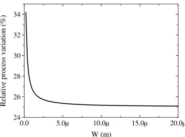
2.3.3 Mismatch analysis ... 33
2.4 Circuit design ... 37
2.5 Experimental results... 38
2.6 Comparison with literature ... 43
2.7 Conclusion ... 45
3. DESIGN OF A LOW POWER; LOW PROCESS SENSITIVE REFERENCE CURRENT GENERATOR ... 47
3.1 Introduction ... 47
3.1.1 Transconductive factor based on a resistance... 47
3.1.2 Transconductive factor based on the MOSFET beta ... 48
4
3.3 Experimental results... 54
3.4 Conclusion ... 58
4.DESIGN OF A LOW POWER, LOW PROCESS SENSITIVE RELAXATION OSCILLATOR ... 59
4.1 Introduction ... 59
4.2 Description of the relaxation oscillator topology ... 61
4.3 Design of the oscillator blocks ... 63
4.3.1 Voltage reference ... 63
4.3.2 Current reference ... 63
4.3.3 Comparators... 63
4.3.4 Latch SR... 66
4.3.5 Switches and capacitors... 67
4.4 Simulation results... 68
5. A METHOD FOR THE ANALYSIS OF THE NUMBERS AND STABILITY OF NON LINEAR LOOP CIRCUITS OPERATING POINTS... 71
5.1 Introduction ... 71
5.2 The proposed method for the determination of the number and stability of circuit operating points ... 74
5.3 Design of a self-biased native-MOSFETs based current generator ... 78
CONCLUSION ... 81
5
SOMMARIO
Il continuo scaling delle tecnologie CMOS pone numerose sfide ai progettisti, relativi alla crescente sensibilità delle grandezze elettriche alle variazioni di processo. Questa problematica riguarda sia la progettazione analogica che quella digitale, e si traduce nel fatto che le prestazioni tipiche dei circuiti non traggono pieno vantaggio dai miglioramenti nominali offerti dalle tecnologie molto scalate. Un’atra importante sfida per i progettisti circuitali è relativa alla progettazione di sistemi per le emergenti applicazioni portatili e impiantabili, come transponder RFID passivi o dispositivi medici impiantabili. Per queste applicazioni sono necessari un consumo di potenza estremamente basso e una ridotta sensibilità delle grandezze di uscita alle variazioni di processo.
Gli approcci proposti per affrontare il problema della variabilità spesso fanno uso sistemi in reazione di complessi e dispendiosi. Per quanto riguarda i circuiti analogici, in alcuni casi vengono utilizzate procedure di trimming ad hoc, che comunque possono essere costose per le applicazioni portatili e impiantabili sopra menzionate. Più recentemente, è stato presentato un metodo basato su una compensazione “interna”, la cui efficacia è abbastanza limitata.
Per questi motivi proponiamo la progettazione di generatori di quantità di riferimento molto precise, basati sull’uso di dispositivi che sono disponibili anche in tecnologia CMOS standard e che sono “intrinsecamente” più robuste rispetto alle variazioni di processo. Seguiamo quindi un approccio “variability-aware”, ottenendo una bassa sensibilità al processo insieme ad un consumo di potenza veramente basso, con il principale svantaggio di una elevata occupazione di area. Tutti i risultati sono stati ottenuti in una tecnologia UMC 0.18µm CMOS:
In particolare, abbiamo applicato questo approccio al progetto di un riferimento di tensione basato sulla classica architettura “bandgap” con l’uso di bipolari di substrato, ottenendo una deviazione standard relativa della tensione di riferimento dello 0.18% e un consumo di potenza inferiore a 70 nW. Questi risultati sono basati su misure su un set di 20 campioni di un singolo batch. Sono anche disponibili risultati relativi alla variabilità inter batch, che mostrano una deviazione standard relativa cumulativa della tensione di riferimento dello 0.35%.
Questo approccio è stato applicato anche alla progettazione di un riferimento di corrente, basato sull’uso della classica architettura bandgap a bipolari e di resistori di diffusione, ottenendo anche in questo caso una sensibilità al processo della corrente di riferimento dell’1.4% con un consumo di potenza inferiore a 300 nW. Questi sono risultati sperimentali ottenuti dalle misure su 20 campioni di un singolo batch.
I riferimenti di tensione e di corrente proposti sono stati quindi utilizzati per la progettazione di un oscillatore a rilassamento a bassa frequenza, che unisce una ridotta sensibilità al processo, inferiore al 2%, con un basso consumo di potenza, circa 300 nW, ottenuto sulla base di simulazioni.
Infine, nella progettazione dei blocchi sopra menzionati, abbiamo applicato un metodo per la determinazione e la stabilità dei punti di riposo, basato sull’uso dei CAD standard utilizzati per la progettazione microelettronica. Questo approccio ci ha permesso di determinare la stabilità dei punti di riposo desiderati, e ci ha anche permesso di stabilire che i circuiti di start up spesso non sono necessari.
6
ABSTRACT
The continuous scaling of CMOS technologies poses several challenges to circuit designers, related to the growing sensitivity of electrical quantities to process variations. This issue involves both digital and analog design, and translates in the fact that circuit performance is typically not able to take full advantage of the nominal improvements offered by aggressively scaled technologies. Another important challenge for circuit designers is related to the design of systems for the emerging portable or implantable applications, such as passive RFID transponders or implantable medical devices. For such applications, extremely low power consumption and low process sensitivity of output quantities are an essential requirement.
Proposed approaches to tackle variability often involve complex and power hungry feedback systems. For what concerns analog circuits, in some cases ad-hoc trimming procedures are envisaged, which however can be very expensive for the above mentioned portable and implantable applications. More recently, a method has been presented based on an "internal" compensation, whose effectiveness is quite limited.
This is why we propose the design of very precise reference quantities generators based on the use of devices that are available also in standard CMOS technology and are "intrinsically" more robust with respect to process variations. We therefore follow a "variability-aware" approach, obtaining a low process sensitivity together with a very low power consumption, with the main drawback of a sizeable increase in chip area. All results are obtained in a UMC 0.18 µm CMOS technology. In particular, we apply this approach to the design of a reference voltage generator based on a "classical" bandgap architecture with the use of substrate bipolar transistors, obtaining a relative standard deviation of the reference voltage of 0.18% and a very low power consumption smaller than 70 nW. These results are based on measurements performed on a set of 20 samples from a single batch. Results related to inter-batch variations are also available, and show a cumulative relative standard deviation of the reference voltage of 0.35%.
This approach is also applied to the design of a current generator, based on the use of a "classical" bipolar-based bandgap architecture and of diffusion resistors, obtaining also in this case a very low process sensitivity of the reference current of 1.4% with a low power consumption smaller than 300 nW. These are experimental results obtained from measurements on 20 samples from a single batch.
The proposed voltage and current generators are then used for the design of a relaxation low-frequency oscillator, which couples a low process sensitivity smaller than 2% with a low power consumption of about 300 nW, as obtained by circuit simulations.
Finally, for the design of the above mentioned blocks, we apply a method for the determination and stability of circuit operating points, based on the use of the standard CAD tools used for circuit design. This approach allows us to determine the stability of the desired operating points, and it also allows us to establish the start up circuits are often not needed.
7
1. PROCESS VARIABILITY IN LOW POWER SCALED CMOS
TECHNOLOGIES
In the last ten years, MOSFETs have reached deep decananometer dimensions: from 2010 Intel and AMD have started producing commercial chips using a 32 nm process (for example Intel processors Core i3, Core i5 and the dual core mobile Core i7). From 2012 a commercial 22 nm technology is used in the Intel Ivy Bridge family of processors. The use of 10-nm MOSFETs with conventional architecture has also been demonstrated in a research environment [1].
The continuous downscaling poses several problems to integrated circuit design, because the advantages of scaling, especially in terms of speed, area occupation (for digital circuits) and costs, come at the cost of a significant increase in power consumption, especially for complex digital systems like processors, and of very large sensitivity of transistor operation to process variations. Challenges are also posed by new emerging applications for integrated circuits in scaled technologies, like portable applications or medical implantable devices. For these kind of systems a low power consumption is necessary, but generally it is obtained with an increase of sensitivity to process variability, as we will see.
Therefore the challenge of the "portable devices era" is to obtain the desired performance, in terms of performance per watt, notwithstanding the increasing relevance of process variability
For digital systems like processors and memories, the main design trade-off is between speed and power consumption. While it can be difficult to obtain a good nominal trade off between these two requirements, process variability can change the operating point of the devices so that the final circuit does not comply with the specifications..
Process variability is usually taken into account in the design phase by performing corner analysis or Monte Carlo simulations, but the increased process variability can lead to an excessive reduction of the design space and to an unacceptable relaxation of other requirements. The problem stems from the fact that both corner and Monte Carlo analysis assume no correlation between different parameters, which is unrealistic and leads to overestimating the process variation and mismatch effects. Moreover, with technologies scaling there is a growth of the number of corners and a widening of their distribution.
These problems require new design techniques and approaches, beyond the traditional tools, in order to meet the nominal requirements in the presence of a large process variability. In digital systems, due to the high computational capability and resources, stability towards process is usually obtained with complex feedback systems which use run-time configurability and adaptive bias, as we will see. In analog circuits, the challenge posed by lowering of power consumption and increasing of process variability is very difficult to solve especially if we consider portable battery-operated devices with limited digital capabilities, for examples implantable medical devices or short-range low frequency communication systems like passive RFID transponders and wireless sensors networks. For these systems reducing power consumption implies an increased sensitivity to process variability, which, should be solved with simple and cheap solutions, so complex
8 compensation feedback or the classical post-processing trimming are not feasible. This is the challenging problem addressed in our thesis.
In what follows we will analyze the effect of scaling for digital and analog circuits, highlighting the growing process variability and the need and the effects of power consumption reduction.
For what concerns process variability, it is important to distinguish between inter-die and intra-inter-die variability. The first one includes lot-to-lot, wafer-to-wafer and a portion of the within wafer variations: it equally affects every element on a chip. Intra-die variability, instead, is related to random and systematic components which produce a non-uniformity of electrical characteristics across the chip. Examples of the lot-to-lot and wafer-to-wafer variations include processing temperatures, equipment properties, wafer polishing and wafer placement [2]. The within-wafer variations are important both for inter-die and intra-die variability. For example, the resist thickness across the wafer is random from wafer to wafer, but deterministic within the wafer, while aberrations in the stepper lens are a cause of (systematic) intra-die variability. An example of random intra-die variability cause is the placement of dopant atoms in the device channel region, which varies randomly and independently from device to device. In the literature, a test chip has been proposed [3] capable of characterizing spatial variations in digital circuits: results from measurements data show that low-voltage domains lead to increased variability, that intra-die variations are uncorrelated and that die-to-die variations are strongly correlated but exhibit decreased correlation as the power supply voltage is lowered.
1.1 Variability-aware low power digital circuits in scaled
technologies
1.1.1 Scaling of technologies and digital circuits
The continuous scaling of technologies poses several challenges to digital integrated circuit design. Indeed, down to the 90 nm node, scaling was accompanied by performance improvements and reduction of power consumption for a given functionality [1]. Scaling also implied a reduction of the intrinsic gate switching delay and an increased integrated circuit density, with consequent cost reduction for the same circuit complexity. The main drawback was the reduction of power supply voltage, which was usually accompanied by a reduction of the MOSFET threshold voltage that resulted in an overall decrease of switching times. If all voltages and all geometrical parameters were scaled by a factor 1/S, this implied an ideal S2 density increase, an ideal 1/S decrease of the intrinsic delay and an ideal 1/S2 decrease in power consumption at a constant power per unit area [4].
However, from 65 nm and below, some physical and quantum mechanical effects, that were previously negligible, become very important and affect devices and circuits performances. The most important consequences of these effects are [4]:
• larger leakage currents;
9 • increased influence of interconnect delay on circuit performance ; • larger gate leakage currents
For what concerns subthreshold leakage current, the current Isub of a MOSFET with
VGS=0 is given by:
−
=
T th subV
V
I
I
η
exp
0 , (1.1)where I0 is inversely proportional to the MOSFET length L. This shows that a lower
threshold voltage and lower sizes implies a larger subthreshold current, also because the threshold voltage reduces for very short transistors lengths.
For what concerns process variability, there are two main effects that increase intra-die variability:
• random dopant distribution [5], [6]; • line edge roughness [7] [8].
Random dopant distribution is related to the intrinsic spread of the number of dopants in the active area [1][9]: the decrease of the channel length and width implies a smaller number of dopants in the space charge regions, and therefore a larger impact of random variations on the total number of dopants. For example the number of dopant atoms in the channel inversion layer for a 0.1 µm feature size MOSFET is on the order of ten, hence, its standard deviation , in the case of a Poissonian process, reaches about 30% [6]. The variation in the number of dopants affects, heavily, MOSFETs threshold voltage [10]. In addition to random discrete dopants in the active region of transistors, it is important to consider also random dopants and grain boundaries in the polysilicon gate [11].
Line edge roughness is caused by tolerances inherent to materials and tools used in the lithography processes. Its importance is related to the fact that, as MOSFET length decreases, the same roughness at the edge of poly lines becomes more relevant, leading to a larger variation in the effective gate length.
In conclusion, digital design in scaled technologies must take into account the increase of power consumption due to the leakage currents and the increase of intra-die process variability.
1.1.2 Low power consumption in digital circuits
Reduction of power consumption is very important for digital systems like processors, because all improvements given by continuously scaled technologies, in terms of speed, devices density and cost, are limited by the continuous increase in power consumption per unit area, which poses problems related to heat removal and cooling and which can prevent circuits from reaching the high performance allowed by scaling.
10 Power consumption in digital circuits can be divided in three main parts: switching power, short circuit power (these two powers constitute the dynamic circuit power) and static leakage power. The total power consumption can be expresses as:
DD leak DD SC DD L
V
I
V
I
V
fC
P
=
α
2+
+
, (1.2)where α is the switching activity (related to the number of commutations during which energy is absorbed from power supply), f is the switching frequency, CL is
the load capacitance, VDD is the supply voltage, ISC is the short circuit current and
Ileak is the static leakage current. From this expression we can easily understand
that an increase of the operating frequency f, allowed by scaling, also implies an increased switching power. Thus far, the most commonly used approach to reduce power consumption is related to the scaling of power supply voltage [13] because this has a quadratic effect on power consumption reduction. However, a reduction in power supply voltage also implies a reduction of speed, so we can use multiple power supply voltages (for example in memories) in order to obtain a good trade-off between these two requirements.
The MOSFETs threshold voltage reduction is useful in order to sustain performance with power supply voltage reduction because it allows to preserve overdrive voltages and MOSFET current drives; however, threshold voltage reduction implies a larger impact of leakage currents on the total power consumption.
In the literature, several techniques have been proposed in order to face the trade off between dynamic power (which can be reduced without performance reduction by lowering power supply voltage and MOSFETs threshold voltages) and leakage power consumption (which increases with the decrease of threshold voltage): we can use subthreshold devices [14], or multi-threshold devices [15]. The latter method can be applied in multiple-threshold technologies and it is based on the use of larger threshold-voltage MOSFETs in non-critical timing paths in order to reduce power consumption.
We can also use adaptive body bias [16] to control threshold voltages for the subthreshold leakage reduction: indeed reverse body bias (an increase of the pMOS n-well voltage with respect to the supply voltage or a substrate voltage reduction related to ground) is an effective technique for reducing the leakage power of a standby mode design [16]. We will better define the adaptive body bias in the next paragraph. It is important to note, however, that as technologies scale down, the bulk factor becomes smaller [4], and this implies that the adaptive bias is not effective in the reduction of power consumption.
In microprocessors we can control power supply voltage in order to reduce power consumption (switching power depends on the third power of Vdd) and we can control the substrate voltage in order to reach a faster speed, for a given power consumption requirement.
1.1.3 Variability-aware low-power digital circuits
Very common requirements for digital circuits such as memories and microprocessors are related to speed and power consumption. Due to process variability, the operating points of the implemented circuits form a "cloud" around
11 the nominal ones, so some dies cannot achieve the desired speed requirement, while others may fail the maximum leakage power specification [2]. Memories are among the most variability-sensitive components of a system, because most of the transistors in a memory are of minimum size and thus are more prone to variability. Additionally, memories are dominated by parallel paths (wordlines and bitlines) hence timing can be severely degraded by variability due to the dominance of a worst-case path over the rest. Finally, if we consider periodic multimedia applications, memories occupy the majority of the chip area and contribute to the majority of the digital chip energy consumption.
Classical worst case corner analysis is overly pessimistic and adds up to a high total safety margin, which may not ensure compliance with all requirements. For this reason, new techniques [17] have been developed to address the process variability problem with no degradation of circuit performance. They are based on a run-time configurability, because they monitor the configuration and/or system clock, detecting timing violations due to process variability, and they tune some circuit parts at run-time with the use of closed-loop control systems, in order to meet the system-level real-time requirements (in this sense they are “self-adaptive” systems). It is important to note that this approach is effective for the reduction of process variability not only related to technology (layers, atomic variations, lithography) or to electrical parameters (threshold voltage, mobility, leakage), but also to time (temperature drift, degradation, aging), because correction is at run-time.
In Fig. 1.1 an example of process variability effects on SoC is shown. Similar considerations are also true for memories [18], related to the requirements of energy and delay for read/write operations, and for microprocessors. Two operating points are considered: a nominal one, with the desired speed and power requirements, and a faster but more power-hungry one. As already said, due to process variability, the nominal operating point becomes a "cloud", so some dies cannot achieve the desired speed requirement. This cloud can also shift due to temperature or aging degradation. Moreover, if we consider temperature effects, some chips may fail the maximum leakage power specification [2]. Speed and power consumption of each circuit are measured and if the actual operating point does not satisfy speed requirements, a run-time knob is used to reconfigure it towards the faster operating point, by increasing power consumption, in such a way
12 Fig. 1.1: SoC with two design points under variability, reliability and temperature
effects, a knob is used to drift the clouds from one design point to another that also considering the cloud due to variability, the desired speed requirement is met [17], [19]. In this process compensation approach circuits are designed for the nominal requirements of speed and power and they are optimized for the typical case, so no overly pessimistic design is considered: the reconfiguration is applied only for troublesome chips and only for the needed time, reaching gains in power consumption of up to 30% or gains in performance of up to 64% [18], according to targeted specification constraints. Alternatively, we can employ a clock frequency control, based on the use of PLLs, which can adjust the clock period to the delay of the slowest component in the system. This relaxing of the clock period requirement is a solution in order not to increase total power consumption, but has a negative impact on the application execution time, due to the slower clock. We can also combine the two techniques in order to obtain the desired functionality minimizing power consumption [19].
The self-adaptive systems approach is based on the use of process monitors in critical sections of the circuits, on the use of a control algorithm and of actuation knobs, which change circuit operating point obtaining a system reconfiguration so as to regain specifications. This implies the presence of tunable circuit parts. In what follows we will discuss in more details the typical monitors, knobs and reconfiguration systems for digital circuits. Process monitors are used in order to detect quantities and parameters affected by process variations and critical from this point of view: since the important requirement for digital circuits, is speed, digital delay timing monitors are typical for these circuits are [17] [20], and are used to measure and predict setup time violations or to detect any significant shift in combinatorial logic delay.
Monitors are usually implemented as replicas of the monitored circuit critical paths [16], [21]. Delay chains, composed of multiple cascaded copies of the same cell, are used to amplify the propagation delay of interest. Alternatively, ring oscillators can be used [22][23]: they are closed-loop delay chains used to provide a periodic signal whose period is proportional to the propagation delay.
Delay chains and ring oscillators measure an average propagation delay, so they can be used in order to detect inter-die and inter-wafer variability, while they are
13 not useful for mismatch measurements. A mismatch detector for MOSFETs threshold voltage has been presented in [24], based on the comparison of the voltage drops on MOSFETs biased with a constant current source. These voltages are converted into a digital signal by means of a VCO followed by digital counters, in order to post process or scan out the threshold voltage measurement.
Some examples of leakage monitors have been proposed [25] [26], [27] [23], which measure on-chip leakage current. This is obtained by properly biasing the MOSFET under test. Indeed the basic principle of leakage sensing is based on the drain-induced barrier lowering (DIBL) [23]: when a high drain voltage is applied to a short-channel device, the barrier height between the drain and the source is lowered, resulting in a decreased threshold voltage and an increased leakage current. Inversely, when a constant bias current flows through a short-channel device, a smaller drain voltage is obtained on a device having a lower threshold voltage. On the basis of these considerations, a MOSFET biased in subthreshold region can be biased with a constant current source, and the leakage can be determined by measuring the drain voltage of the MOSFET itself. This can also be used to measure slew rate [28]. However, leakage-based sensing methods can suffer from on-chip temperature variations, especially in high-performance applications.
Some examples of knobs are:
• the circuit power supply voltage (this technique is called “dynamic voltage scaling” (DVS));
• the MOSFET transistor substrate voltage (this technique is called “adaptive body bias” (ABB));
• the power supply voltage together with the substrate bias (it has been shown that this control is more effective than the two previous individual controls for low-power high-performance microprocessors [29]);
• the control voltage of a PLL system which adaptively changes the system clock frequency [19].
The control of the power supply voltage Vdd can be efficiently used for the reduction of power consumption, as already said, but a low Vdd implies a significant performance degradation. In microprocessors, for example, frequency can be controlled through an adaptive change of the supply voltage, so can be also used to compensate process-induced frequency variations. However, since both switching and leakage components of power consumption have a super-linear dependence on power supply voltage, the change of Vdd can have a significant impact on the total power consumption [29].
For what concerns adaptive body bias, which has been presented as a technique for the reduction of power consumption, it is also an important way to control and to reduce process variability effects. The substrate voltage can be controlled in two ways:
• “Reverse body bias” (RBB): we use a pMOS well voltage larger than the power supply voltage or an nMOS substrate voltage smaller that the ground (or the negative power supply) voltage, with a consequent
14 increase of the MOSFET threshold voltage. It is used to reduce the circuit power consumption even at the cost of a lower speed.
• “Forward body bias” (FBB): we use a pMOS well voltage smaller than the power supply voltage or an nMOS substrate voltage larger that the ground (or the negative power supply) voltage. It is used to increase speed because it reduces the threshold voltage, at the cost of a larger power consumption.
We can also apply a bidirectional adaptive body bias (ABB), which means that we can lower the MOSFET threshold voltage for slow MOSFETS (FBB) and we can increase the threshold voltage for MOSFETs with a large leakage (RBB). In fact, if we consider digital circuits like microprocessors, while reverse body bias can be an effective way to reduce the maximum power consumption, however it does not affect the maximum circuit delay and so its minimum speed. On the other hand, forward body bias is effective in improving the minimum circuit speed [30]. The substrate voltage control poses some problems, for example the clusterization of MOSFETs with the same threshold voltage.
Monitors and knobs are used in closed-loops reconfigurable systems: for example in [30] a speed-adaptive threshold voltage CMOS scheme is presented, in which substrate bias is controlled so that critical paths delay in a circuit remains constant. The simplified view of this scheme, which can be considered an example of typical adaptive systems for digital delay control, is shown in Fig. 1.2.
Fig.1.2: adaptive system for digital delay control
The feedback system is composed by a delay line, a comparator, a decoder and the body bias generators, which also control the propagation delay of the delay line. The comparator measures propagation delays between an external clock signal and the output signal from the delay line. The amount of delay is encoded and converted in an analog value which controls the bias generators, in such a way as to maintain a constant delay of the delay line, corresponding to the external
15 clock frequency at equilibrium. This delay line is usually a replica of the circuit with the most critical path.
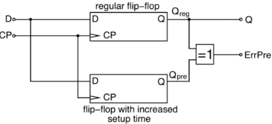
The approach based on the use of replica circuits in a feedback loop is useful for the compensation of inter-die and inter batch variability, as already said [31]. However, scaling implies increased intra-die process variability, which limits the effectiveness of a global voltage control. For this reason several techniques [32], [33] have been proposed for an in-situ characterization of circuit blocks with small hardware overhead. For example [32] proposes local supply voltage adjustment for systems sub-blocks which are made over-critical: indeed a flip-flop with increased setup time is inserted in parallel to a regular flip flop (see Fig. 1.3), at the end of sub-block critical paths. Outputs of both flip flops are compared: when there is a timing failure for the increased setup time flip-flop (where it occurs first), an error prediction signal (ErrPre in Fig. 1.3) is triggered, which is used by a control logic in order to change the power supply voltage of the sub-block. An in-situ characterization is capable of taking all kinds of process variations, random, within die and die-to-die, as well as environmental and transient variations, into account. There is obviously a trade-off between the advantages in terms of process variability reduction, and the area and power consumption overhead due to the presence of over-critical flip flops.
Fig. 1.3: basic structure of a flip flop for critical timing detection
1.2 Variability-aware low power analog circuits in scaled
technologies
1.2.1 Scaling of technologies and analog circuits
We already said that scaling is advantageous for digital circuits, even if in sub nm technologies new problems arise which must be addressed by means of new techniques. For analog circuits, advantages and disadvantages of scaling are not so evident: scaled technologies are used in mixed-signal systems, where they offer advantages especially for the digital section. Also for analog circuits, however, an
16 advantage of scaling is the availability of transistors with higher speed, which can be used in RF circuits and high-speed analog blocks like data converters.
For analog circuits, scaling does not imply an area occupation reduction, because the area of transistors is chosen for noise, linearity or mismatch constraints. A decade-old work presents a detailed analysis of scaling effects for analog circuits [34]: it shows that MOSFET transistors improve with technologies scaling, and this implies also a low power consumption. On the other hand, the supply voltage decreases, and this implies a significant increase in power consumption in order to obtain the same signal to noise and distortion ratio over a certain signal bandwidth. The overall effect is that power consumption decreases with newer CMOS processes down to about 0.25 µm. In sub nm CMOS, either circuit performance decreases or power consumption increases.
1.2.2 Low power consumption in analog circuits
We already said that in digital circuits power consumption is related to the power supply voltage, so we can obtain a low power consumption by properly reducing line voltage. For analog circuits the reduction of power consumption is obtained with different techniques because it is not related to power supply voltage, but to SNR (Signal to Noise Ratio) requirements. In the following, we will derive an expression useful to underline the relation between power consumption and SNR of a circuit. We will consider linear circuits, so the main source of distortion is due to either voltage or current limitations, which produce slewing and/or clipping of the output signal. In a class A system, we start considering the expression for the minimum bias current Ibias in order to prevent slewing, which must be equal to the maximum signal current required to drive the output capacitance C. It can be expressed as [34]:
fCV
I
bias=
2
π
, (1.3)
where f is the signal frequency and V is its magnitude. The thermal noise related to the output node can be expressed as
C
KT
v
=
, (1.4)where K is the Boltzmann constant and v is the root mean square noise associated with the node voltage. So, if we consider relations (3) and (4), the required load capacitance for a specified SNR is:
2
/
2
kT
V
SNR
C
=
⋅
. (1.5)If the supply voltage is equal to the peak-to-peak value of the signal, the minimum power consumption P for class A systems is:
f
SNR
kT
VI
17 For class B systems, the absolute minimum power consumption is a factor π lower than the limit given by (6) for class A systems. From expression (6) we can note that the minimum power consumption for an analog circuit is only related to the signal frequency and to the desired SNR, while it is not dependent on power supply voltage, if the input signal is rail-to rail. However, if the peak-to-peak value of the input signal is smaller than the line voltage, and if we call ∆V the part of the supply voltage not used for signal swing, we can express the minimum power consumption P as:
V
V
V
f
SNR
kT
VI
P
dd dd bias∆
−
⋅
⋅
⋅
=
=
2
8
π
. (1.7)From (1.7) we can note that in this case the minimum power consumption is larger than in the case of a rail-to-rail input signal. In every case, the minimum power consumption is directly proportional to the desired SNR, so analog circuits become less power efficient when the desired SNR increases, independently of technology and of the power supply voltage.
The power consumption indicated by (1.6) and (1.7) is a theoretical value, which is increased considering:
- the power consumption of the bias circuit, which also adds to the output noise; - the presence of additional noise sources, related to internal circuit components or to the power supply voltage, which imply an increase in power consumption in order to maintain the same SNR;
- the use of large devices (in order to reduce their mismatch), which adds to the total parasitic capacitance.
We already said that for systems that are not rail-to-rail there is a slight dependence of power consumption on the power supply voltage. Also the presence of a power consumption related to the bias circuit implies that a line voltage reduction can be helpful for in a power consumption reduction. These are the reasons why also in analog circuits the trend is toward a power supply voltage reduction. This reduction, together with the power consumption reduction, can be successfully obtained with the use of MOSFETs operated in subthreshold or weak inversion.
In subthreshold (or weak inversion) the relation between MOSFET drain current ID and its gate-to-source voltage VGS is exponential and it is expressed as:
−
−
−
=
T DS T th GS T DV
V
V
V
V
V
I
2exp
1
exp
η
β
, (1.8)where VT is the thermal voltage, Vth is the MOSFET threshold voltage, η is the
subthreshold slope and β is the product between carrier mobility µ, gate oxide capacitance for unit area COX and MOSFET width W divided by MOSFET length L.
In weak inversion the minimum drain-to-source voltage in order to ensure saturation is lower than in strong inversion, because it is equal to the a small multiple of the thermal voltage. In addition, in weak inversion the
18 transconductance-to-current ratio of a transistor reaches its maximum value. This implies a maximum gain-bandwidth product for a given load capacitance when the current is limited or a minimum input-equivalent noise for a given output noise. In a differential pair, it implies the maximum gain per device and the minimum input-referred offset. However, the maximum value of the transconductance-to-current ratio of a MOSFET implies also a maximum mismatch of current mirrors, which is directly proportional to the MOSFET transconductance, for a given current, and a higher noise, because the drain current noise spectral density is proportional to the drain-source conductance, and proportional to the MOSFET transconductance. Finally, the transition frequency in weak inversion is lower than a few hundred MHz also for 0.18 µm CMOS, so it can not be used in high frequency analog applications.
1.2.3 Low power applications for analog circuits
Low power requirements are extremely demanding for emerging classes of applications, such as short-range low frequency communications systems, like RFID or wireless sensors networks, and biomedical implantable devices. These applications require small size and small weight, and require battery-operated systems with extremely low power consumption to minimize battery replacing or recharging, which can be very expensive or not practical, for example in the case of medical devices
1.2.3.1 Wireless sensor networks
A wireless sensor network consists [35] [36] of one or more base stations and a number of autonomous sensor nodes, from ten to thousands. These nodes are distributed in a physical space in order to monitor physical or environmental parameters. A wide variety of mechanical, thermal, biological, chemical, optical, acoustic and magnetic sensors may be attached to the sensor node. Each node is composed by one or more low-power sensing device, a limited memory and an embedded processor which is interfaced with the sensor, a power module and a radio transceiver, so it has capabilities of sensing, data processing and wireless communication. Wireless communication is used to minimize the infrastructure and to access otherwise inconvenient locations. The measured physical data are processed and transmitted through the network to the base station with the use of a wireless communication channel, so each node can share the collected and processed information through the series of wireless links between nodes, and the end-user can extract the collection of data gathered by several nodes. Depending on the application, actuators may be incorporated in the sensors [37].
One of the first applications for wireless sensor networks was in military environment, for example for the military target tracking and surveillance, because they can help in intrusion detection and identification [38].They can also monitor friendly forces, equipment and ammunition, they can be used for battlefield surveillance and nuclear, biological or chemical attack detection and reconnaissance [37]. Sensor nodes can also be used in environmental applications, for example for chemical or biological detection, for agriculture, or for the forest fire detection. Some applications in the context of seismic sensing have been proposed [39]. They are very useful in industrial application and especially in logistics, asset tracking and supply chain management [40][41].
19 With technology advances, sensor nodes can also be used for domotic applications, allowing the development of a smart environment self-adapting to the needs of the end user [42]. The concept of "ambient intelligence" [43], which is an environment sensitive and adaptive to people needs, can be applied in the contexts of homes, cars, and offices.
An important and emerging application of WSN is also biomedical and health monitoring [44]. In this field, they are also called body sensor networks (BSN) [45], and they are used for a continuous and non-invasive monitoring of health body parameters and physiological signals, such as temperature, heart rate, electrocardiogram (EKG/ECG), physical activity and respiration. Some examples of SoC platforms for the ubiquitous medical monitoring have been proposed, with very low power consumption [46] [47].
The data rate requirements of WSN are quite low because, especially if we consider environmental or health monitoring, changes are slow and so data rate is low.
A sensor node, as already said, is made up of four basic components [37]: a sensing unit, a processing unit, a transceiver unit and a power unit. The first unit consists of sensors and an analog front end interface with the internal blocks. Usually the first stage consists of an LNA with proper gain and high SNR, and analog-to-digital converters. The low output rates of sensors allow ultra low power amplifier design with devices operating in weak inversion. The processing unit, which is generally associated with a small storage unit, executes data processing and manages the communication protocol. The transceiver unit connects the node to the network. For what concerns communication, even the most energy efficient transceiver standards in commerce, for example those associated with the IEEE 802.15.4 and IEEE 802.11 physical layers, have power consumption of the order of tens of mW.
Wireless sensors networks nodes must have low sizes, in such a way to be embedded in the environment. They must also be low-cost to enable the realization of sensor networks with a large number of nodes, and this implies that the single node, the communication protocol and the network design must have low complexity to satisfy the low cost requirement. Finally they must have a very low power consumption, of the order of 100 µW, because nodes, which are typically battery operated, are in large number and they can be inserted in difficult to access location, so they must be energetically autonomous, because the battery replacing or recharging can be very difficult. Low power consumption must be obtained at each level of the system design, from the physical layer to the communication protocol (for example the operating range of each node is limited to a few meters and the data rate is limited to a few kbps).
1.2.3.2 Implantable medical devices
Implantable medical devices [48] monitor and treat physiological conditions within the body. Some example are hearing aids [49], pacemakers, implantable cardiac defibrillators, glucose meters, drug delivery systems and neurostimulators, which can help the treatment of hearing loss, cardiac arrhythmia, diabetes, Parkinson's disease.
20 The sensors of body area networks are also an example of implantable medical devices [50] for medical diagnostics. They are used in order to continuously measure internal health status and physiological signals.
These applications require wireless devices with small size and weight, and with low power consumption. Security and safety are also very important requirements. In fact, if we consider BSN, it is important for the communication to be reliable, secure and energy-efficient, and the network must be protected against injection or modification of measurements transmitted to the external devices. 1.2.3.3 RFID
Radio Frequency Identification (RFID) is a contactless technology for automatic identification and tracking which uses radio frequency communication. An RFID system is composed by a reader and a tag (or transponder) located on the object to be identified. RFIDs are relatively small and cheap and they are widely used [51] in asset tracking, real time supply chain management [52] and telemetry-based remote monitoring. They are also used for access control to buildings, parking [53], public transportation and open-air events, airport baggage, animal identification, express parcel logistic. The need for high volume, low cost, small size and large data rate is increasing, while stringent regulation of transmit power and bandwidth have to be met.
RFID systems are closely related to smart cards, because data (the identification information) is stored on an electronic device (the transponder), but their advantages with respect to smart cards are the fact that power supply to the transponder and data exchange with the reader is contactless: this circumvents all the disadvantages related to faulty contacting, so sabotage, dirt, unidirectional insertion, time consuming insertion, etc...
The RFID reader typically contains a radio frequency transceiver, a control unit and a coupling element to the transponder, while the latter is generally composed of a coupling element and an electronic microchip. An important classification of transponders is based on the type of power supply:
- active transponders have an on board battery which provides the power supply voltage;
- semi-passive transponders have an on board battery which however only supplies the logic and the memory management unit, while the reader radiated field is used for transmission, with the modulated backscattered radiation technique; - passive transponders receive all power needed from field radiated from the reader. A fraction of such power is used by the transponder to communicate with the reader by modulating the backscattered radiation.
Both active and passive transponders benefit from a low power supply voltage: for the first ones, this implies longer battery lifetimes or smaller batteries sizes; for the second ones, this implies a longer communication distance (which can be up to a few meters).
Passive transponders with electromagnetic coupling operate in the UHF (868 MHz in Europe and 915 MHz in USA) or microwave range (2.45 GHz or 5.8 GHz). UHF transponders commercially available need to have about 150 µW input power, and reach a reading distance of 2-8 m, depending on the antenna and operating frequency. If we consider active transponders, the operating range can reach 15 m. The simplified view of a passive RFID transponder is shown in Fig. 1.4 [54].
21 Fig. 1.4: simplified view of a passive RFID transponder
The system is composed by an external antenna (for example a printed loop antenna), which is power matched with the average input impedance of the voltage multiplier. The voltage multiplier is used in order to convert a part of the incoming RF signal into a dc power supply voltage for the internal transceiver blocks. The demodulator converts the pulse-width modulated input signal to digital data and generates a synchronous system clock. The transmission from transponder to reader (uplink) is based on modulating the backscatter of the continuous wave carrier transmitted by the base station. The changes in the IC input impedance are related to data from the control logic. The logic circuit handles the protocol, including anti-collision features, cycling redundancy checksums, error handling, enabling and disabling of analog circuits. A charge pump converts the dc supply voltage into the higher voltage needed for programming the EEPROM; it works at a frequency of approximately 300 kHz generated by an on-chip RC oscillator. The EEPROM contains the transceiver information, for example the identifier.
Further improvements in RFID systems in order to increase the operating range and/or the battery lifetime are related to a proper choice of the modulation technique or to the use of extremely low voltage and low power circuits.
1.2.4 Variability-aware low power analog circuits
The problem of process variability is relevant and challenging also for analog circuits. For example, [55] analyzes the distribution of the MOSFET drain current considering three different batches for the same 90 nm CMOS technology, showing a broad distribution of the current considering the same batch (mainly due to intra die variability), and a very different mean value from batch to batch.
This problem becomes more relevant if we consider subthreshold circuits, given the exponential relation between voltage and current.
Different techniques can be used in order to reduce process variability in analog circuits:
• trimming;
22 • analog compensation circuits.
Trimming is a very common technique used in order to obtain high-precision
output quantities, for example in reference voltage generators. It is a post-processing technique, which is based on the measurement of the error between the actual output quantity and the desired value, and on subsequent error correction through the tuning of a dedicated correction circuit. For example, if the output quantity is a current, the current mirror can be composed of additional branches which can be properly activated or deactivated in order to adjust the output quantity to minimize the error. The activation can be done with the help of a digital section including programmable fuses or memories. Another alternative is the use of laser [56] to adjust resistances. Another post-processing technique [57] in order to reduce the effects of process variations is based on the use of configurable transistors, which are composed by a certain number of parallel MOSFETs with switch-connected gates. The configuration of these switches, achieved through digital signals, provides a mechanism to adjust the overall device size. Configurability is used for transistors which are the most sensitive to process variations. In present day industrial design, however, the tendency is to avoid trimming, except for very precise blocks, such as reference generators, since post-processing is usually quite expensive.
Similar to digital trimming is the digitally enhanced analog design [58], whose aim is to leverage digital correction and calibration techniques to improve analog performance. The difference with respect to trimming is that in this case the calibration is at run time and is implemented with a digital section that controls the analog quantities and acts on the analog circuit in order to improve precision and stability towards process. It is a technique similar to the one applied in digital adaptive systems, previously described. Indeed digital calibration is obtained [59] with systems composed by an error-revealing node, an error configuration, and a compensation node. In the error-revealing node a signal is measured that is only function of the error we have to compensate. The error configuration is the condition with which we reveal the error and the compensation node is the node in which we insert a compensation signal, which reduced the error. For example, MOSFET bias currents can be digitally controlled and programmed [60] [61] using current mode ladder structures in order to compensate for process variations and components mismatch. The digital signal processing is used also to overcome shortcomings of analog design [62], for example in order to obtain digital calibration of A/D converters [63], [64], [65]. Digital enhancement techniques can be successfully applied also to power amplifiers [66], because they allow an improvement in linearity with a gain in power efficiency of the system. For example, in [67] it was shown that replacing opamps with open-loop gain stages and nonlinear digital correction can reduce amplifier power dissipation by 3-4 times. Digitally enhanced analog design, however, is useful if a digital section is present, while it can be a very expensive solution for applications such as passive RFID transponders, sensors networks or biomedical devices, where the digital section is not present or it is very simple. For these applications, an analog compensation technique is more convenient.
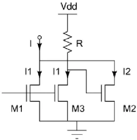
In the recent literature [55], an alternative technique to trimming or to digitally enhanced circuits has been proposed. It only uses analog circuits with a proper compensation technique, based on the use of reverse correlated quantities. For
23 example in [55] the design has been proposed of current sources whose reference current is obtained as the sum of two reverse-correlated currents. The principle of operation is illustrated by the circuit in Fig. 1.5.
Fig. 1.5: addition-based current generator
The reference current is the sum of the saturation currents of MOSFETs M1 and M2 (I1 and I2, respectively). If current I1 increases, also the voltage drop across R increases, reducing the gate-to-source voltage of M2, and therefore reducing current I2. In this way the sum current I remains almost constant.
In order to obtain a process-invariant reference current, we must have:
2 1 2
2
gm
I
V
gs∆
−
=
∆
(9)which requires that resistance R is equal to 2/gm2. With this approach, authors
obtain with experiments a reduction of the relative standard deviation of the reference current from 11% to 6.5%, but still high in absolute value. Better results have been obtained with the same approach applied to the design of ring oscillators [68], where authors obtain a reduction of the oscillation frequency relative standard deviation of more than 65%, even if it is still of about 6%.
Another interesting example of process compensation analog loop is presented in [69], where a MOSFET threshold monitor is used in an adaptive biasing circuit in order to obtain a process-dependent control voltage for a process and temperature compensation of a clock oscillator. With this approach authors obtained an oscillation frequency very stable towards process, with a worst-case variation, considering process and temperature, of 2.64%. However the compensation mechanism is quite complex and it can add too much to total power consumption,
24 especially if we consider the previously mentioned RFID transponders and implantable devices.
1.3 Organization of the thesis
The problem of process variability in analog circuits becomes more and more important with the continuous scaling of technologies. Proposed solutions to mitigate it involve the use of digitally enhanced circuits or trimming, which however may be very expensive, considering systems with a limited or almost absent digital section, such as passive RFID transponders and implantable devices. For such kind of applications, a completely analog solution is preferable. The use of complex feedback systems is not effective, since they imply increased power consumption, while low power is an important requirement for these applications. The use of simple circuits which implement a compensation technique, such as the ones proposed by [55][68], may not be so effective, if very precise quantities are necessary.
This is why we propose an alternative approach, based on the use of devices which are intrinsically more stable towards process and which are available also in standard CMOS technologies, such as lateral bipolar pnp transistors and diffusion resistors. We apply this approach to the design of reference quantities (voltage, current and frequency) generators. With a proper design, we will show that we are able to obtain both extremely low sensitivities to process and a very low power consumption, with the main drawback of a large area occupation.
In Chapter 2 we propose the design of a reference voltage generator with extremely low process sensitivity and very low power consumption. The voltage generator uses substrate bipolar pnp transistors in a "classical" bandgap architecture, that as we will demonstrate is the best solution to obtain stability towards process. With a proper design, we meet this requirement together with the lowest power consumption when compared with bandgap generators proposed in literature. The main drawback is a large increase in area occupation. We made intensive statistical analysis on the reference voltage, considering two Silicon batches.
In Chapter 3 we propose the design of a reference current generator with very low process sensitivity. It is based on a bandgap architecture with the use of diffusion resistors, that represent one of the best options to minimize sensitivity to process variations. This requirement is coupled to very low power consumption, obtained with a proper design. Also in this case, the main drawback is a large increase in area occupation. We made statistical analysis on the reference current, considering a single silicon batch.
In Chapter 4 we propose the design of a relaxation oscillator, which uses the proposed voltage and current generators to obtain stability towards process. This is obtained together with low power consumption. The performance of the proposed oscillator is verified by simulations, because a silicon run is currently under fabrication.
In Chapter 5 we will propose a technique for the analysis of non linear loop circuits, which is useful also for the design of the previously mentioned blocks. This technique is very fast, simple and accurate, because it uses DC analysis of
25 commercial circuit simulators, and allows us to determine the number and the stability of circuit DC operating points. It also allows us to assess when it is necessary to include start up circuits. This technique has been successfully applied to the design of a current generator with the use of native transistors. Experimental results validate the usefulnessof the method.
26
2. DESIGN OF A LOW POWER, LOW PROCESS SENSITIVE
REFERENCE VOLTAGE GENERATOR
2.1 Introduction
The reference voltage generator is an important building block for a wide range of analog and mixed signal circuits, such as A/D converters, DRAMs, flash memories, low dropout regulators and oscillators. It generates a reference voltage which has to be stable against process, temperature and line variations. The new kind of applications discussed in Chapter 1, such as implantable systems or passive and semi-passive transponders, also demand for a very low power consumption, because the reference voltage can be considered as a bias circuit, so its power consumption does not contribute to bandwidth or SNR of an analog system.
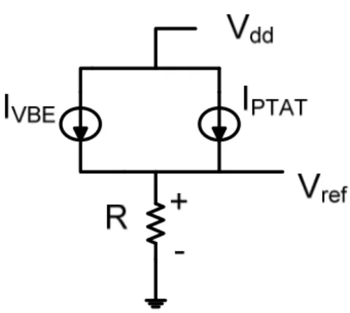
Until ten years ago, most reference voltage generators were based on a bipolar bandgap architecture proposed by Widlar in 1974 in [70], that achieves a very robust voltage against process, temperature and line variations, and is based on the principle illustrated in Fig. 2.1.
The reference voltage is obtained as the sum of two terms:
PTAT BE
ref
V
RI
V
=
+
, (2.1)Fig. 2.1. Scheme of a bandgap voltage reference: a) Voltage mode. b) Current mode.
where VBE is the base-emitter voltage of the bipolar transistor Q1. The temperature
compensation is obtained by adding to VBE, which has a negative temperature
27 design parameters, Vref can have a very low temperature sensitivity (as low as 11
ppm/°C [71]). In the standard bipolar bandgap voltage reference, the term RIPTAT is
obtained from the difference between the base-emitter voltages of two bipolar transistors operating with different current densities [70]. This architecture is also very useful in order to obtain a reference voltage with low process sensitivity (the typical relative standard deviation of the reference voltage is close to 1% [72][73]). The main drawback is represented by the difficulty to use a low power supply voltage. Indeed, to achieve temperature compensation, Vref must be close to Egap/q ~ 1.2 V, where Egap is the silicon gap and q is the elementary charge [70].
This however implies that the reference voltage is "anchored" to the silicon energy gap, which is a physical property very stable towards process, and therefore enables to achieve a reference voltage with very low process sensitivity.
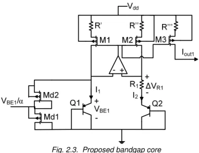
However, modern low-power low-voltage circuits need reference voltages well below 1 V. Several techniques have been proposed in order to design sub-1 V CMOS bandgap references [74]. Among them, a remarkable one is based on the bandgap principle but with a proper topology, in which compensation occurs by summing two currents, instead of two voltages, with opposite temperature coefficients. The drawback is a noisier reference voltage because of the contribution of noise due the current mirrors [71]. The principle is shown in Fig. 2.2, where IVBE indicates a current proportional to the base-emitter voltage of a bipolar transistor, and was proposed by Banba et al. [75].
Fig. 2.2. Scheme of a bandgap voltage reference current mode.
It is based on the observation that even if the voltages in the bandgap generator are relatively large, currents can be made very small by properly choosing high resistance values, and can be effectively used for temperature compensation (the obtained temperature sensitivity is of about 120 ppm/°C). This however implies a trade off between power consumption and area occupation. In particular authors obtained a current consumption greater than 1 µA with a large area occupation of