DOCTORATE OF RESEARCH IN INDUSTRIAL CHEMISTRY
XXI CYCLE
Scientific Sector: CHIM/04
DEVELOPMENT AND CHARACTERIZATION OF
NON-OXIDE CERAMIC COMPOSITES
FOR MECHANICAL AND TRIBOLOGICAL
APPLICATIONS
A Doctoral Thesis by
Laura Silvestroni
Coordinator:
Supervisor:
Prof. Luigi Angiolini
Prof. Giuseppe Palombarini
Supervisors at ISTEC-CNR:
Dr. Diletta Sciti
Dr. Stefano Guicciardi
A mio babbo,
che aveva un’inventiva stravagante e continua a prendersi cura di me
TABLE OF CONTENTS
ABSTRACT 12
LIST OF PUBLICATIONS RELATED TO THIS THESIS 15
AIM OF THE WORK 16
LITERATURE REVIEW
CHAPTER 1 – ADVANCED CERAMIC MATERIALS 18
1.1 Introduction 18
1.2 General properties of advanced ceramics 19
1.3 Production of advanced ceramic materials 21
1.3.1 Starting materials 21
1.3.2 Synthesis and powder processing 22
1.3.3 Moulding 23
1.3.4 Sintering mechanisms 25
1.3.5 Sintering technologies 28
1.3.6 Finishing 31
1.4 SiC- based ceramics 32
1.5 Ultra High Temperature Ceramics 33
References 35
CHAPTER 2 – ANALYSIS TECHNIQUES 36
2.1 Microstructural characterization 36
2.1.1 X-ray powder diffraction 36
2.1.2 Scanning electron microscope 38
2.1.3 Transmission electron microscope 42
2.1.3.1 Components 42
2.1.3.2 Imaging 47
2.1.3.4 Modifications 54
2.2 Mechanical and tribological characterization 55
2.2.1 Hardness 55 2.2.2 Elastic modulus 57 2.2.3 Nanoindentation 59 2.2.4 Fracture toughness 62 2.2.5 Flexural strength 64 2.2.6 Wear 66 2.3 Electrical characterization 71 2.3.1 Electrical resistivity 71 References 73
SECTION I: SiC – BASED CERAMICS 74
CHAPTER 3 – SILICON CARBIDE:
FEATURES AND UTILIZATION 75
3.1 Introduction 75
3.2 Chimical-physical features 76
3.2.1 Crystal structure 76
3.2.2 Stability and transformation 78
3.3 Synthesis 82
3.4 Sintering 83
3.4.1 Solid state sintering 83
3.4.2 Liquid phase sintering 84
3.5 Mechanical properties 90
3.5.1 Strength 90
3.5.2 Fracture toughness 91
3.6 Applications of SiC-based ceramics 92
CHAPTER 4 – SECONDARY PHASE: MoSi2 100 4.1 Introduction 100 4.2 Physical properties 102 4.3 Sintering of MoSi2 103 4.4 Mechanical properties 104 4.4.1 Hardness 104 4.4.2 Strength 105 4.4.3 Fracture toughness 105 4.5 Oxidation 106 4.6 MoSi2composites 108 4.7 Applications 110 References 112 EXPERIMENTAL PROCEDURE CHAPTER 5 – SiC-COMPOSITES
PRODUCTION AND CHARACTERIZATION 114
5.1 Mixtures composition 114
5.2 Powder processing 117
5.3 Sintering 117
5.4 Characterization 117
References 123
RESULTS AND DISCUSSION
CHAPTER 6 – MICROSTRUCTURE
AND MECHANICAL PROPERTIES 124
6.1 Introduction 124
6.2 Sintering behaviour 125
6.3 Microstructure 127
6.4 Mechanical properties 134
6.5.1 Disc on pin tests 141
6.5.2 Slider on cylinder tests 144
6.6 Electrical properties 152
References 153
CHAPTER 7 – CONCLUSIONS I 154
SECTION II: UHTCs MATERIALS 157
LITERATURE REVIEW
CHAPTER 8 – UHTCs: FEATURES AND UTILIZZATION 158
8.1 Introduction 158 8.2 Chemical-physical features 159 8.3.1 Structural stability 159 8.3.2 Structure 162 8.3.3 Thermodynamical properties 163 8.3 Processing 164 8.3.1 Sintering 164 8.3.2 Machining 166 8.4 Main properties 167 8.4.1 Thermal properties 167 8.4.2 Mechanical properties 170 8.4.3 Electrical properties 173 8.4.4 Optical Properties 174
8.5 High temperature testing 175
8.6 Applications 178
8.7 Recent works 180
References 182
CHAPTER 9 – UHTCs PRODUCTION AND CHARACTERIZATION 184 9.1 Mixtures composition 184 9.2 Powder processing 185 9.3 Sintering 185 9.4 Characterization 186 References 189
RESULTS AND DISCUSSION
CHAPTER 10 –MICROSTRUCTURE
AND DENSIFICATION MECHANISMS 190
10.1 MoSi2addition to UHTCs 190
10.2 ZrC-based composites 192 10.2.1 Introduction 192 10.2.2 Sintering behaviour 193 10.2.3 Microstructure 194 10.3 HfC-based composites 198 10.3.1 Introduction 198 10.3.2 Sintering behaviour 199 10.3.3 Microstructure 199
10.4 Densification mechanisms of Zr- and Hf- Carbides 202
10.5 ZrB2-based composites 208 10.5.1 Introduction 208 10.5.2 Sintering behaviour 208 10.5.3 Microstructure 209 10.6 HfB2-based composites 213 10.6.1 Introduction 213 10.6.2 Sintering behaviour 214 10.6.3 Microstructure 214
10.7 Densification mechanisms of Zr- and Hf- Borides 218
References 223
CHAPTER 11– RESULTS AND DISCUSSION:
MECHANICAL PROPERTIES AND OXIDATION 225
11.1 Mechanical properties 225 11.1.1 ZrC -based materials 225 11.1.2 HfC -based materials 227 11.1.2.1 Nanoindentation 231 11.1.3 ZrB2-based materials 234 11.1.4 HfB2-based materials 238
11.2 Arc jet oxidation 242
11.2.1 Introduction 242
11.2.2 Plasma flow characterization 243
11.2.3 Microstructure modification 245
11.2.4 Cataliticity evaluation 248
11.2.5 Conclusions 250
References 252
CHAPTER 12– TERNARY COMPOSITES 254
12.1 HfB2-based ternary composites 254
12.1.1 Introduction 254
12.1.2 Densification behaviour 254
12.1.3 Microstructure 255
12.1.4 Mechanical properties 261
12.1.5 Conclusions 264
12.2 ZrC-based ternary composites 264
12.2.1 Introduction 264
12.2.2 Densification behaviour 264
12.2.3 Microstructure 265
12.2.5 Conclusions 271
References 272
CHAPTER 13– CONCLUSIONS II 273
ABSTRACT
Keywords: carbides, borides, silicides, densification, microstructure, mechanical properties.
The main reasons for the attention focused on ceramics as possible structural materials are their wear resistance and the ability to operate with limited oxidation and ablation at temperatures above 2000°C. Hence, this work is devoted to the study of two classes of materials which can satisfy these requirements: silicon carbide -based ceramics (SiC) for wear applications and borides and carbides of transition metals for ultra-high temperatures applications (UHTCs).
SiC-based materials: Silicon carbide is a hard ceramic, which finds applications in many industrial sectors, from heat production, to automotive engineering and metals processing.
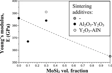
In view of new fields of uses, SiC-based ceramics were produced with addition of 10-30 vol% of MoSi2, in order to obtain electro conductive ceramics.
MoSi2, indeed, is an intermetallic compound which possesses high temperature
oxidation resistance, high electrical conductivity (21·10-6 Ω·cm), relatively low density
(6.31 g/cm3), high melting point (2030°C) and high stiffness (440 GPa).
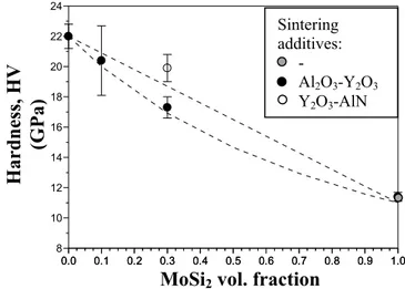
The SiC-based ceramics were hot pressed at 1900°C with addition of Al2O3-Y2O3 or
Y2O3-AlN as sintering additives. The microstructure of the composites and of the
reference materials, SiC and MoSi2, were studied by means of conventional analytical
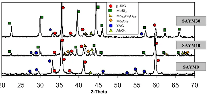
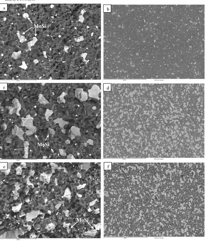
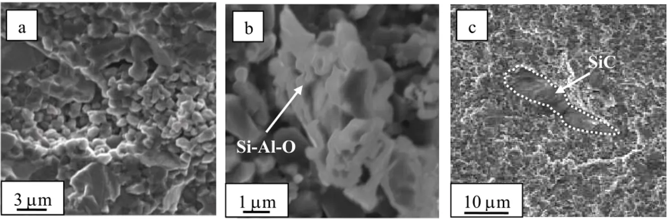
techniques, such as X-ray diffraction (XRD), scanning electron microscopy (SEM) and energy dispersive spectroscopy (SEM-EDS). The composites showed a homogeneous microstructure, with good dispersion of the secondary phases and low residual porosity.
The following thermo-mechanical properties of the SiC-based materials were measured: Vickers hardness (HV), Young’s modulus (E), fracture toughness (KIc) and
composites were compared to those of two monolithic SiC and MoSi2 materials and
resulted in a higher stiffness, fracture toughness and slightly higher flexural resistance. Tribological tests were also performed in two configurations disco-on-pin and slider-on cylinder, aiming at studying the wear behaviour of SiC-MoSi2 composites with
Al2O3 as counterfacing materials. The tests pointed out that the addition of MoSi2 was
detrimental owing to a lower hardness in comparison with the pure SiC matrix.
On the contrary, electrical measurements revealed that the addition of 30 vol% of MoSi2, rendered the composite electroconductive, lowering the electrical resistance of
three orders of magnitude.
Ultra High Temperature Ceramics: Carbides, borides and nitrides of transition
metals (Ti, Zr, Hf, Ta, Nb, Mo) possess very high melting points and interesting engineering properties, such as high hardness (20-25 GPa), high stiffness (400-500 GPa), flexural strengths which remain unaltered from room temperature to 1500°C and excellent corrosion resistance in aggressive environment. All these properties place the UHTCs as potential candidates for the development of manoeuvrable hypersonic flight vehicles with sharp leading edges.
To this scope Zr- and Hf- carbide and boride materials were produced with addition of 5-20 vol% of MoSi2. This secondary phase enabled the achievement of full dense
composites at temperature lower than 2000°C and without the application of pressure. Besides the conventional microstructure analyses XRD and SEM-EDS, transmission electron microscopy (TEM) was employed to explore the microstructure on a small length scale to disclose the effective densification mechanisms. A thorough literature analysis revealed that neither detailed TEM work nor reports on densification mechanisms are available for this class of materials, which however are essential to optimize the sintering aids utilized and the processing parameters applied.
Microstructural analyses, along with thermodynamics and crystallographic considerations, led to disclose of the effective role of MoSi2 during sintering of Zr-
and Hf- carbides and borides.
Among the investigated mechanical properties (HV, E, KIc, σ from room temperature
to 1500°C), the high temperature flexural strength was improved due to the protective and sealing effect of a silica-based glassy phase, especially for the borides.
Nanoindentation tests were also performed on HfC-MoSi2 composites in order to
extract hardness and elastic modulus of the single phases.
Finally, arc jet tests on HfC- and HfB2-based composites confirmed the excellent
oxidation behaviour of these materials under temperature exceeding 2000°C; no cracking or spallation occurred and the modified layer was only 80-90 µm thick.
LIST OF PUBLICATIONS RELATED TO THIS THESIS
1 D. Sciti, L. Silvestroni, A. Balbo, S. Guicciardi, G. Pezzetti, “High–strength and – toughness electroconductive SiC-based composites”, Advanced Engineering Materials 8 No. 10 (2006) 997-1001.
2 D. Sciti, A. Bellosi, “High density pressureless sintered HfC-based composites”, Journal of the American Ceramic Society 89 Issue 9 (2006) 2668-2670.
3 S. Guicciardi, L. Silvestroni, G. Pezzotti, D. Sciti, “Depth-sensing indentation hardness characterization of HfC-based composites”, Advanced Engineering Materials 9 No. 5 (2007) 389-392.
4 L. Silvestroni, D. Sciti, “Effects of MoSi2 additions on the properties of Hf- and
Zr-B2 composites produced by pressureless sintering”, Scirpta Materialia 57 (2007)
165-168.
5 L. Silvestroni, D. Sciti, A. Bellosi, “Microstructure and properties of pressureless sintered HfB2-based composites with additions of ZrB2 or HfC”, Advanced
Engineering Materials, 9, No 10 (2007) 915-920.
6 S. Guicciardi, L. Silvestroni, C. Melandri, D. Sciti, G. Pezzotti, “Nanoindentation characterization of HfC-based composites”, International Journal of Surface and Engineering 1, N. 2/3 (2007) 198-212.
7 D. Sciti, L. Silvestroni, A. Bellosi, “Properties of Pressureless Sintered (Hf, Zr) Borides and Carbides with Additions of MoSi2”, Proceedings of the 31th
International Conference on Advanced Ceramics and Composites, January 2007 Cocoa Beach, Florida.
8 R. Savino, M. De Stefano Fumo, L. Silvestroni, D. Sciti: Arc-jet testing on HfB2and HfC -based Ultra-High-Temperature-Ceramic Materials, Journal of the
European Ceramic Society 28 (2008) 1899–1907.
9 D. Sciti, L. Silvestroni, “Microstructure and properties of pressureless sintered ZrC-based materials”, Journal of Materials Research 26 No. 7 (2008) 1882-1889. 10 S. Guicciardi, C. Melandri, L. Silvestroni, D. Sciti, “Indentation grid analysis of
nanoindentation bulk and in situ properties of ceramic phases”, Journal of Materials Science 43 No. 12 (2008) 4348-4352.
11 L. Silvestroni, D. Sciti, J. Kling, S. Lauterbach, H-J. Kleebe, “Sintering Mechanisms of Zirconium and Hafnium Carbides doped with MoSi2”, accepted at
Journal of American Ceramic Society.
12 L. Silvestroni, D. Sciti, S. Lauterbach, H-J. Kleebe, “Transmission electron
microscopy on Zr- and Hf-borides doped with MoSi2: mechanisms of
16
AIM OF THE WORK
The possibility to obtain new materials which possess good thermo-mechanical properties and wear resistance is a common demand in many fields of technological research and in industrial sectors.
The availability of materials with improved performances implies a better and more efficient functioning of many technological systems thus leading to new applications, new processes and to improved uses of the disposable sources.
In the last decades, much effort has been done in the field of advanced ceramics thanks to the broad spectrum of possible applications and to the uniqueness of their properties. In this branch, silicon carbide-based materials constitute a class of very promising structural materials for engineering application such as components operating at high temperature or in aggressive environment, engine parts, heat exchanger and wear resistant materials.
Besides SiC-based materials, a new class of materials with interesting engineering properties is arising always more interest in the scientific community. These materials, labelled Ultra High Temperature Ceramics (UHTC), can withstand temperature above 1600°C in aggressive environment. In addition to high melting points, UHTCs possess extremely high melting temperatures and a unique combination of chemical stability, high electrical and thermal conductivities and resistance to erosion and corrosion that make them suitable for extreme environments associated to hypersonic flights, atmospheric re-entry and rocket propulsion.
This work is composed by two sections: the first deals with silicon carbide-based materials, the second with ultra high temperature ceramics. The materials were produced from commercial powders, the pellets were sintered by hot pressing or pressureless sintering and finally they were characterized by microstrucutral and thermo-mechanical analysis.
17
part I: to develop electroconductive SiC-based electroconductive materials with improved mechanical properties and good wear behaviour;
part II: to obtain ceramics with a controlled microstructure which show good mechanical properties even at temperature of 1500°C and oxidation resistant.
An outline of the performed activity is reported below.
The majority of this work was carried out at the Institute of Science and Technology for Ceramics – National Research Council (Istec-CNR) of Faenza.
Part of the wear analyses on SiC-based materials was performed at the Department for Metals Science, Electrochemical and Chemical Techniques of the Faculty of Industrial Chemistry of Bologna.
TEM analyses on UHTCs were performed at the Department of Materials Science at the Technnische Univestität Darmstadt, Germany.
Arc-jet tests on UHTCs were performed at the Department of Aerospace Engineering of the University of Napoli.
Literature review
Experimental procedure
Literature review Experimental procedure
Literature review
Introduction to advanced ceramic materials Chapter 1 Analysis techniques and testing methods Chapter 2
SiC-based ceramics
Features and utilizations Chapter 3
Secondary phase Chapter 4
Materials production Chapter 5
Results and discussion Chapter 6
Conclusions I Chapter 7
UHTCs materials
Features and utilizations Chapter 8
Materials production Chapter 9
Results and discussion Chapter 10, 11
Ternary composites Chapter 12
Conclusions II Chapter 13
SECTION I
CHAPTER 1
ADVANCED CERAMIC MATERIALS
1.1 INTRODUCTION
Until recently, materials for advanced structural applications have been largely restricted to advanced metallic alloys. However it now appears that for certain applications, mainly those involving high temperatures, metallic materials have reached the limit for their potential development. In combustion engines and other energy generating equipment, the desirability of higher operating temperatures has driven the development of Ni-, Co- and Fe-based alloys to extreme levels of sophistication in microstructural and structural design. However, such development is necessarily limited by the melting point of these materials. For further development, ceramics offer one of the few avenues to a significant increase in service temperatures. Their low density, chemical inertness and high hardness offer additional potential for extending performances limits beyond those offered by metallic materials. Hitherto, the widespread use of ceramics has been inhibited by their brittleness and poor reliability of strength. To overcome these problems, considerable progress has been made during the past two decades in the compositional and microstructural design of ceramics. The application of the composite principle has been the most important advance in this field, for example, the combination of two or more constituent phases with appropriate microstructural morphology in a material brings to a combination of improved properties.1
The definition of ceramics given by Warren1 is the following:
Ceramics can be defined as chemically stable, inorganic, crystalline, non-metallic compounds or mixture of such compounds.1
The bonds set by the above definition are flexible. A large number of compounds with high melting point, notably the carbides, nitrides, borides and silicides of the transition
metals are borderline ceramics. They often exhibit metallic character being electrically conducting and having poor chemical resistance. They are nevertheless of interest as matrix in ceramic composites. Some examples of ceramics and currently used composites are listed with the most significant properties in Tab. 1.I.
Tab. 1.I: Materials and properties of some ceramics of industrial interest.
Material δ Tm E ν cond Th. α ρ KIc HV resistance Wear
g/cm3 °C GPa W/mK K-1 0-103°C (25°C) Wm MPam1/2 GPa KIc3/4H1/2 Al2O3 3.99 2050 390 0.23 6.0 8.0 >1015 3-5 19 10-14.5 SiC 3.2 2500 440 0.15 40 4.5 ~1 3.4 26 12-15 Si3N4 3.2 1900 300 0.22 15 3 - 4-6 16 10-15 B4C 2.5 2450 440 0.18 15 5.5 0.5 3.7 45 17.9 BN h ┴ 2.3 3000 45 - 21 7.5 1011 - 5 - AlN 3.3 2300 320 0.25 50 6 1012 2.7 13 7.6 TiB2 4.5 2980 570 0.11 25 5.5 10-5 5-7 30 21 TiC 4.9 3070 450 0.18 30 8.5 10-4 4 30 15.5 TiN 5.4 3090 - - 30 8.5 10-5 - 20 - MoSi2 6.3 2100 440 0.17 20 8.5 10-5 5 13 11.8 ZrO2 t 6.1 2400 - - 2 12 - 5-10 12 11.5-20 ZrO2 m 5.6 - 240 0.3 - 15 - 1 - - mullite 2.8 1850 150 0.24 5 5.5 - 2 15 6.5
The chemical bonds of ceramic is generally hybrid of covalent and ionic, the proportions of which vary from compound to compound. The characteristic properties resulting from such bonding are, for example, high melting point, high chemical stability, high elastic modulus and low atomic mobility, the latter leading to high hardness and creep resistance but also to brittleness.
1.2 GENERAL PROPERTIES OF ADVANCED CERAMIC MATERIALS
Ceramics can be classified into different groups depending on chemical composition, microstructure and application.2 From the application point of view, the main difference has to be done between traditional and advanced ceramics.
The traditional ceramics include tableware, pottery, sanitary, ware, tiles, bricks and clinker.
The advanced ceramics include functional ceramics and structural ceramics. The former have been developed and are primarily used for non-mechanical properties such as
thermal insulation, electrical resistance/conductivity, etc. whereas the latter have been developed for application able to bear various forms of mechanical loading, for example high temperature strength and conditions of wear and erosion.
Some fields of application of advanced ceramics are listed in Tab. 1.II. Tab. 1.II: Fields of application of some advanced ceramics.
Field Required properties Materials Examples
Engine manufacturing
Wear resistance, heat and electrical insulation, low density, resistance to corrosion,
high temperature strength
Al2O3,
ZrO2,SiC,
Si3N4
Thermal insulation of combustion chambers, valve seats,
spark plugs, turbochargers, gas turbine Industrial processing engineering Resistance to corrosion, wear resistance Al2O3, SiC, C (graphite), ZrO2
Chemical devices, drawing die, slide rings, thread guides, rolls for
paper industry High temperature
techniques
Resistance to corrosion, thermal and electrical insulation, high temperature
strength
Si3N4, SiC,
Al2O3, C, BN,
MoSi2, ZrB2
Heat exchangers, crucibles, heating conductors, protective tubes
for thermocouples, loading devices for materials testing, burner units Machining of materials Resistance to corrosion, wear resistance Al2O3, Si3N4,SiC, B4C, TiC, TiN, BN, diamond
Cutting tools, grinding wheels, sandblast nozzles Medical devices physiological compatibility Resistance to corrosion, Al2O3, ZrO2 Bone replacement (hip joints), dental ceramics
Electrical engineering
electronics
Electrical insulation, heat
conductivity Al2O3, AlN Substrates for integrated circuits, insulations
The advanced ceramics can be further distinguished among: • silicate ceramics,
• oxide ceramics, • non-oxide ceramics.
This classification is a mixture of chemical composition (oxide/non-oxide) and atomic structure (glassy-amorphic/crystalline). The main feature of silicate ceramics is the glassy-amorphic phase with a pronounced pore structure. The main content is SiO2 with
addition of Al2O3, MgO, BeO, ZrO2 and other oxides.
Oxides ceramics are distinguished from silicate ceramics by the dominance of a crystalline phase with only a small content of glassy phase. The most important oxides are: Al2O3, BeO, MgO, ThO2, TiO2, UO2, ZrO2.
elements carbon in the form of graphite and diamond, nitrides AlN, BN, Si3N4, TiN
carbides B4C, SiC, TiC, WC, ZrC, HfC, TaC
borides TiB2, ZrB2, HfB2
silicides MoSi2, TaSi2
sialons Si3N4 with Al2O3
syalons Si3N4 with Al2O3 e Y2O3.
1.3 PRODUCTION OF ADVANCED CERAMICS
Advanced ceramic materials are characterized by high and specific level of mechanical and functional performances. The achievement of such performances requires a step of design in which the microstructural and functional characteristics and the cost of production have to be taken into consideration. In the case of the advanced ceramic materials, a deep knowledge of the relationships between process, microstructure, and functional properties is necessary. The whole processing has to be optimized in each steps in such a way as to obtain the desired properties.
The processing of ceramics is developed in several stages: choice of raw materials
powder treatment moulding
thermal treatment finishing
Each of these phase is critical, as each of them can be source of flaws or imperfections in the materials which sum each others up and hinder the achievement of the desired properties.
1.3.1 Starting materials
The raw material are of great importance to get high quality ceramics. The correct evaluation of the appropriate starting powders is critical because, as it is the starting point of the industrial process, it will determine the features of the final product. For
high performances materials strict characteristics are requested. An example of requirements for a typical high performances ceramic is reported in Tab. 1.III.
The purity of starting powder is of essential importance for high temperature behaviour, because impurities may segregate at grain boundary, provoke creep and sliding of amorphous phases and lower the mechanical properties at high temperature. The dimensions are relevant too for the final density of a compact: they should have an optimal size distributions in order to fill the voids and leave the least porosity as possible during the densification. Besides, particles with a high specific surface possess a high free Gibbs energy which is thermodynamically favourable and brings to the decrease of the specific surface area through the densification. Then, finer powders allows the decrease of time and temperature necessary for sintering, thus hindering the grain coarsening.
Tab. 1.III: Characteristics and requirements of starting powders for high performances prodoucts.
Particles dimensions Small
Particle size distributions Tight
Particles shapes (usually) regular and spherical
Agglomerates As low as possible
Specific surface High
Reactivity High Chemistry composition Homogeneous impurities Absent stoichiometry Full phases Stable
1.3.2 Synthesis and powder processing
The addition of organic or inorganic additives to the starting powder is often necessary as a function of the following processes and of the desired quality in the final products. The additives can be organic binder, necessary to favour the transition from a powder to a semi manufactured which withstands to handling, lubricants, which favour moulding and pressing operations, plasticizers, which allow the development of plastic deformations, dispersants, that increase the stability of colloidal suspensions, antistatic agents, antifoam agents or inorganic additives which favour the densification.3
1.3.3 Moulding
During the moulding stage, powders opportunely treated, are consolidated through different techniques in a green compact. This hand-manufactured is characterized by a high degree of porosity that depends on the kind of the utilized powder, on the underwent treatment and on the particular moulding technique, it generally goes from 50 to 70% of the theoretical density. Through this process the ceramic component is preformed depending on the final application to whose is destined. The objective of this process, beyond giving a shape to the component, is to obtain a high degree of density in the green compact, without cracking and with a homogenous distribution of the porosity. The handmade deriving from the performing is quite brittle and has to be handled with care, nevertheless it has to be transportable and it has to guarantee the workability. For a lot of applications, it might be necessary indeed to obtain ceramic with particular and complex shapes which require the machining of the green before being subjected to the following sintering treatment.
Many shapes can be obtained with various techniques briefly explained in the following.
Pressing
• Uniaxial pressing: the compacting occurs in a stiff die through the application of a unidirectional pressure. It can be a dry or damp process depending on the amount of humidity lower or higher than 4%. Often binder are added to improve the adhesion of the particles and lubricant to increase the sliding of the particles and so optimizing the packaging. Powders with a high fluency are those obtained through spry drying. Further improvement in this step can be achieved when the die is subjected to ultrasonic pulse during the filling. In this way porosity and big defects can be removed with subsequent increase in the homogeneity. • Cold isostatic pressing: it consists of the application of pressure in a
uniform way in each direction. The pre-compacted powder is placed in a rubber die, immersed in a fluid (glycerine, hydraulic oil, water,…) into a pressure chamber. The fluid transfers the pressure to every part of the die in a uniform way. The deformation of the die is followed by a
compacting of the powder. Also in this case moulding additives, such as lubricant and binder, are used. By this techniques high pressure (more than 500 MPa) can be achieved; by cold isostatic pressing more complex shapes can be obtained then by uniaxial pressing.
Slip casting
A ceramic suspension is poured in a porous chalk die, when the suspended particles sediment and the die absorbs the liquid phase, a final solid component is obtained. To improve the sedimentation of the particle this process can be carried out under pressure or in vacuum, otherwise the sedimentation is accelerate through centrifuge of the die and ultrasounds.
Tape casting
A fluid mixture composed of ceramic powder, organic or aqueous additives (solvent, binder, plasticizer,…) is poured on a tape, generally celluloid made, while it flows. Thanks to the presence of two doctor-blades, a film of controlled thickness, varying from 200 to 1.3 mm, can be obtained. By this method it is possible to get a variety of supports or multilayered ceramics.
Injection moulding
This technology is a variation of polymers moulding processes. A ceramic powder, opportunely mixed with organic binders, assume a paste aspect. When this compound is heated to temperature above the softening temperature of the binders, is injected into the cavities of the die, where it is cooled and solidifies. A debonding treatment is necessary to remove the binders.
Extrusion
The extrusion process derives from the metallurgical processes. A mixture of ceramic powder and polymeric additives is rendered homogeneous into a cylinder in vacuum which removes air and bubbles from the mixture, then it is driven into the extrusion chamber through a Archimedes screw and extruded in the desired shape.
Electrophoresis
This technique exploits the properties of very fine particles in solution which becomes electrically charged by adsorption of ions on the surface. Under the action of an electric field, the particles migrate to the electrode-die of opposed charge, they set in and increase the component thickness which will be then sintered.
1.3.4 Sintering mechanisms
Because of the high melting point of oxide and non-oxide ceramics, the processing of ceramics requires a heat treatment, during which a powder is consolidated in a dense compact which possesses desired properties and shape. Even if the main objective is the compacting and the elimination of the pores from the green, the control on microstructure is a crucial problem. Studies on sintering deal with the understanding of the process variables as temperature, holding time, particles dimensions and shapes and sintering environment which all contribute to the final microstructure. All the properties of the ceramics, as mechanical and electrical properties, are strongly influenced by the sintering treatment.
The sintering process can be seen as a coordinate variation of the shape of all the grains of a compact powder activated by matter transport mechanisms which allow to fill interparticle voids. The centre of the grains moves the ones along the others thus reducing their dimensions and removing the porosity in the material. In Fig. 1.1 is schematized this principle which gives a full density material with the smallest specific interfacial area.
The sintering process brings to a compact material, by the reinforcement of adjacent particles bonds and the removal of porosity. To activate the mass transfer mechanisms (diffusion or creep) and a energy source which sustains the transport (heat, thermal gradient) are needed. The driving force is represented by the diminishing of the Gibbs free energy linked to the decrease of the total volume of the component.
When an atom is transferred from the boundary to a pore, this last shrinks because is partially filled: the free energy decreases as the interfacial surface among the grains later decreases. This mechanism can be expressed by the equation (1):4
dGF = γs dAs + γb dAb +p dV (1)
where:
dAs: variation of the total area of the pores;
dAb: variation of the total surfacial area of the grain boundaries;
γs and γb: specific surfacial area of the pores and of the grains respectively:
p: external applied pressure;
dV: volume variation due to shrinkage.
Three different sintering processes can be outlined depending on composition and the amount of the secondary phases which form during densification. These are: solid state sintering, liquid phase sintering and vitrification.
Solid state sintering: the preformed green is thermally treated at temperature ranging from 0.7 to 0.9 of the melting point. Any liquid phase is present and the solid state atomic diffusion produces necks between the particles and progressively eliminates the porosity. A sketch of the solid state sintering process is reported in Fig. 1.2.
Fig. 1.2: Densification phenomena among grains during solid state sintering.
Initial
Intermediate stage
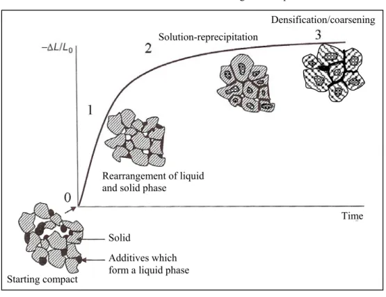
Liquid phase sintering: is classically defined as sintering involving a particulate solid and coexisting liquid during the sintering process. The liquid can result from melting of one component or formation of an eutectic due to the interaction of two or more components. The liquid may be transient or persistent during sintering depending on the solubility relationships. The fundamental requests for a good matter transport and so a good densification are the presence of a liquid phase at the sintering temperature, a good wettability of the solid and a good solubility of the solid into the liquid. Three different stages can be distinguished as shown in Fig. 1.3: rearrangement, solution-reprecipitation, skeleton sintering. The mechanisms of liquid phase sintering have been extensively discussed by Kingery.5 Classically, the following sequence of sintering stages is thought to be prevailing.
Particle rearrangement - Densification results from particle rearrangement under the influence of capillary forces and the filling of pores by the liquid phase. Due to this mechanism, during the early stage of sintering a much faster densification occurs than in solid state sintering. Parameters like volume fraction of the liquid, solubility, green density, temperature, wetting, etc., strongly affect this step.
Solution-reprecipitation - Consequences of the solution-reprecipitation processes are microstructural development, shape accommodation and grain growth. Due to the chemical potential gradient generated by capillary forces, smaller grains dissolve in the liquid and through diffusion, the mass is transported to the larger grains where it re-precipitates. This process is known as Ostwald ripening.6 The process alters the grains shape, which re-accommodate, reduce the porosity and hence shrinkage and densification take place.
Solid-state or skeleton sintering - The last stage is referred to as solid state controlled sintering. The overall shrinkage and densification is very sluggish due to the rigidity of the solid skeleton that inhibits further rearrangement, although microstructural coarsening continues by grain boundary diffusion.
Ceramics sintered by liquid phase sintering have as advantage, the possibility to be near-net shaped, but on the other side, show low creep resistance at high temperature, because of the softening of amorphous grain boundary phases.
Fig: 1.3: Scheme of the different stage of the liquid phase sintering which shows the
microstructural evolution of a green compact.
Vitrification/glazing: during the sintering the porosity is filled by a liquid mixture, about 25 vol%, that vitrifies when under cooled. This method is more used in traditional ceramics, for advanced ceramics is avoided as it brings unhomogeneity and most of all to poor mechanical properties.
1.3.5 Sintering technologies
Several sintering technologies will be briefly described.
Traditional sintering: a green component is subject to a thermal cycle and a holding time in a determinate temperature. It can be performed in air, under vacuum or in controlled environment. In this study, a graphite furnace (ASTRO Thermal Technology Inc, see Fig. 1.4) is mainly utilized which can achieve a maximum temperature of 2100°C and the heating is through graphite heating elements.
Additives which form a liquid phase Solid
Rearrangement of liquid and solid phase
Time Solution-reprecipitation
Densification/coarsening
Fig. 1.4: The furnace ASTRO Thermal Technology Inc.
Reactive sintering: Synthesis and sintering of the product occur at the same time during the heating treatment. For example in the case of silicon nitride, a preformed green of silicon is placed in a furnace and react with flowing nitrogen at temperature around 1200°C. Nitrogen penetrates in the porous structure and gives rise to silicon nitride. Consolidation and densification take place at the same time. Hot pressing: while the temperature increases, a uniaxial pressure is applied to a
pre-compacted powder in order to accelerate the densification. The process occurs under vacuum or in a controlled environment. This techniques allows to record the shrinkage of the material as a function of time and temperature, by the relative movement of the rams. By this way the sintering process can be controlled and the process parameters can be modified during the hot pressing. The collected data are utilized for kinetic studies. An example of a hot pressing, principle of functioning and apparatus, is reported in Fig. 1.5.
Hot isostatic pressing: during the heating of the component a uniform pressure is applied in all the directions. The inner pressurization is obtained by gases as nitrogen or argon, which act on the powder previously sealed under vacuum with a metallic or glassy sheath which is impermeable to the same gas.
Self-propagating high-temperature synthesis: it’s a particular case of the previous method. An electric arc is switched on through a powder mixture in air or in a controlled environment which triggers an exothermic chain reaction propagating at velocity of 0.1-20 cm/sec and self-sustaining. Temperatures of 3500°C can be
achieved. This techniques is quite economical thanks to its fastness and the absence of a continuously fed furnace.
Fig. 1.5: Hot pressing: a) complete apparatus, b) chamber and rams.
Explosive compacting: a green compact is placed in a cylindrical crucible externally covered with an explosive charge. The detonation is lightened at one of the extremity of the crucible, this generates a shock wave, which propagates along the axis of the cylinder thus radially compressing the material. The main drawback is the high amounts of defects and cracks in the final product.
Microwave sintering: thanks to the high dielectric constant of ceramic materials, the sample is heated from inside, in spite of furnish heat from outside. The precompacted sample is invested by a radiation of suitable wave length which produces a thermal flow and the densification occurs at higher speed than in the
a Vacuum chamber Heating elements Insulating elements Load cell Sample Ram Die Hydraulic ram motive-power b
previous cases. This technique allows high heating rates, but it’s difficult to achieve a high degree of uniformity in the sample. It was observed indeed that high microwave frequencies tend to preferably heat the external part of the compact. A solution to this problem is to utilize multi-frequency microwave generators which lead to higher homogeneity during heating.
Spark plasma sintering: a direct current passes through the precompacted powder in a graphite crucible at 5000-20000 A, depending on the sample dimensions, with an applied pressure of 10-100 MPa. By this technique it is possible to obtain very hig heating rate of the order of 600°C/min or even higher. The sintering mechanisms involved in this process are still a matter of discussion but the most diffused opinion is that the plasma formed around the particles notably increase the densification rates and the diffusive processes in such a way that the densification requires holding time of few minutes and lower temperatures with respect to conventional techniques.7-10 A drawn of the apparatus is reported in Fig. 1.6.
Fig. 1.6: Spark plasma sintering apparatus.
1.3.6 Finishing
Even if modern sintering techniques allow to obtain near net shape products with no need of further machining, in most cases the processing furnishes materials which posses slightly irregular shapes or need surface finishing. A good state of finishing can be obtained through a series of techniques as machining with diamond tools, which is expensive and takes long times, laser machining or electron discharge machining, if
Graphite Pulsating current generator Vacuum chamber Sample Load
the material is conductive. This last techniques, EDM, exploits discharge phenomena between an electrode (cathode) and the same rough material (anode) divided by a thin layer containing a dielectric fluid. This stage of machining is long, complex and expensive and can notably influence the final performances of the component. As a matter of fact, cutting operations or machining of sintered materials often generate surface flaws which have to be taken into account before the employ.
1.4 SiC-BASED CERAMICS
Silicon-carbide-based ceramics are promising materials for applications in gas turbine components, heat exchangers, and wear-resistant components. Most of these applications require good strength and toughness, high thermal conductivity and good environmental stability at high temperature.
Silicon carbide was first synthesized in 1891 by Acheson by passing an electric current through a mixture of carbon powder and clay. The material was originally thought to be a mixture of carbon and corundum (aluminum oxide) and trademarked
Carborundum. Acheson soon determined that it was actually silicon carbide. The
product was an immediate commercial success as an abrasive.11 The Acheson process is still the major production process. In the US, over 115,000 metric tons of silicon carbide were produced in 1994 with a value estimated at $40 million, much of which was for abrasives and metallurgical uses.12
Although silicon carbide can fulfill requirements of high strength, one major problem is that SiC hardly densifies without additives, because of the covalent nature of Si-C bonding and the low self-diffusion coefficient. Solid state sintering at temperature around 2100°C was a routine process to densify silicon carbide. The pressureless consolidation of this material was pioneered by Prochazka, who found that small additions of boron and carbon drastically improve the shrinkage kinetics of SiC.13 Following the basic developments, a variety of sintering additives were studied during the past decades, including boron and B-compounds, aluminium and Al-compounds and Be-compounds, all being used in combination with carbon. An innovative approach to pressureless sintering of silicon carbide was initiated in the early 1980 with addition of
oxides to promote the densification of SiC via a liquid phase. Wide variety of rare-earth oxides were investigated in combination with alumina and/or boron compounds to densify SiC and dense and fine materials were obtained without excessively high processing temperatures.14-16 Materials with improved sinterability and room-temperature strength around 700 MPa were obtained by careful optimization of the processing, sintering additives and sintering cycles.16 However, the major problems encountered with this class of liquid-phase sintered materials are the low fracture toughness and the degradation of strength at high temperature. The relatively low toughness (3 MPa⋅m0.5)16 is caused by a fine equiaxed microstructure, which does not
provide any crack deflection or crack bridging phenomena. On the other hand, the high-temperature strength is degraded by the softening of residual secondary phases deriving from the sintering aids.
During the past 30 years, many different aspects have been explored, such as the
fundamental properties of SiC, powder production, porous and dense SiC and
amorphous thin films for applications in electronics. It was found that SiCpossesses a unique combination of properties, such as high strength at ambient and high temperatures, good thermal shock resistance due to a low coefficient of thermal expansion, relatively good resistance to oxidation compared to other high-temperature structural materials, high wear resistance and high thermal conductivity. In addition, the density of SiC is only about 40% of superalloys. This combination of properties makes it possible for SiC to replace metallic components that are conventionally used as structural materials.
Since some aspects of the production of dense SiC-based materials are still critical, considerable efforts are continuously addressed to find and optimize sintering aids and processing.
1.5 ULTRA HIGH TEMPERATURE CERAMICS
The need for high temperature materials that can maintain mechanical strength and operate with limited oxidation at temperatures >2000°C have driven the development of a variety of ceramics and ceramic composites. These refractory materials have come to
be known as Ultra High Temperature Ceramics (UHTCs).17 The earliest work on UHTCs began in the 1960’s by ManLabs under a research program funded by the Air Force Materials Research Lab (AFML). Compared to the other refractory compounds such as carbides and nitrides, ManLabs determined that intermetallic diboride compounds offer the highest degree of oxidation resistance. In comparison to carbides and nitrides, diborides also have high thermal conductivity which gives them good thermal shock resistance. Through further studies, HfB2 and ZrB2 were chosen as the
most promising candidates for use in high temperature applications. It was shown that all UHTCs are characterized by very strong bonding which gives them high temperature structural stability. It also makes them very difficult to fabricate and, so far, only limited research has involved these materials despite their potentialities. Conventional hot pressing of pure UHTCs typically yields porous materials with poor mechanical properties. But the addition of sintering additives helps the densification thus obtaining materials with strengths higher than 500 MPa. Work by ManLabs demonstrated that SiC additions to UHTC powders improved densification and increased oxidation resistance of the composites. High temperature oxidation testing was conducted in both furnace studies as well as in simulated re-entry environments (arc jet) and gave excellent results. After the ManLabs work, further research on UHTCs slowed until the early 1990’s when NASA Ames renewed efforts. Work there resulted in two hypersonic flight experiments, SHARP-B1 and SHARP-B2 that proved the successful application of monolithic high temperature ceramic composites on sharp leading edges. Since then, NASA Glenn has also started conducting research to further improve UHTC oxidation resistance. Current work by the Navy is also seeking to provide a better understanding of the oxidation of not only ZrB2 and HfB2 but HfC, ZrC and HfN as well. Clearly, the
potential applications for UHTCs span a wide number of needs arising from future military, industrial and space based projects. While continued work has provided valuable insight on the performance of UHTCs, consistent ongoing research efforts are required if future applications are to be realized.
References
1 R. Warren, “Ceramic-matrix composites”, BLACKIE, USA: Chapman & Hall, New York. 2 D. Munz, T. Fett, “Ceramics- Mechanical properties, Failure behaviour, Materials Selection”,
Eds: R. Hull, R. M. Osgood, H. Sakaki, A. Zunger, Materials Science, Springer (1999) 3. 3 A. Bellosi, rapporto interno n.87270 CNR IRTEC Faenza.
4 A. Bellosi, rapporto interno n. 03/90 CNR IRTEC, Faenza.
5 W. D. Kingery, H. K. Bowen, D. R. Uhlmann “Introduction to Ceramics”, 2nd Edition, New York, John Wiley, Academic Press, (1960).
6 W. Ostwald, “Lehrbuch der Allgemeinen Chemie”, vol. 2, part 1. Leipzig, Germany, (1896). 7 J. R. Groza, A. Zavaliangos, Mat. Sci. Eng., A287 (2000) 171-177.
8 D. S. Parrera, M. Tokita and S. Morica, J. Eur. Ceram. Soc., 4 (1998) 401-404.
9 L. Gao, H. Z. Wang, J. S. Hong, H. Miyamoto, K. Miyamoto, Y. Nishikawa, S. D. D. L. Torre, J. Eur. Ceram. Soc., 19 (1999) 609-613.
10 L. Gao, H. Wang, H. Kawaoka, T. Sekino and K. Niihara, J. Eur. Ceram. Soc., 22 (2000) 2149-2152.
11 Parche, M. C., “Fact about Silicon Carbide”, The Carborundum Company, Niagara Falls, NY 1961.
12 Ault, N. N., and Crowe, J. T., Silicon Carbide, Ceramic Bulletin, 5, (1991)70.
13 S. Prochazka, Proceedings of the Conference on Ceramic for High Performance Applications (Hyannis, MA, 1973) Ed. By J. J. Burke, A. E. Gorum, R. M. Katz. Brook Hill Publishing Co., (1975) 77-13.
14 F. K Van Dijen and E. Mayer, J. Europ. Ceram Soc. 16 (1996) 413.
15 E. W. Dressler and R. Riedel, Int. J. Refractory Metals and Hard Materials, 15 (1997) 13. 16 L. K. Falk, J. Europ. Ceram. Soc.17 (1997) 983.
17 M. J. Gash, D. T. Ellerby, S. M. Johnson, “Ultra High Temperature ceramic composites” in “Handbook of Ceramic Composites”, ed by Narottam P. Bansal, NASA Glen Research Center, USA, (2005) Kluwer Academic Publishers, Boston.
CHAPTER 2
ANALYSIS TECHNIQUES
2.1 MICROSTRUCTURAL CHARACTERIZATION
Microstructure can be defined as the whole compositional, crystallographic, morphological and texitural characteristics of the phases constituting a material. Studying microstructure means analyzing chemical composition, crystallographic phases, quantity, spatial distribution and mean grain size of the constituting phases, and the presence of flaws into a material.
The analytical techniques that will be performed in the present work are X-Ray Diffraction (XRD), Scanning Electron Microscopy (SEM) and Transmission Electron Microscopy (TEM). A description of the principle is given in the following sections for each technique.
2.1.1 X-ray powder diffraction
X-ray scattering techniques are a family of non-destructive analytical techniques which reveal information about the crystallographic structure, chemical composition, and physical properties of materials and thin films. These techniques are based on observing the scattered intensity of an X-ray beam hitting a sample as a function of incident and scattered angle, polarization, and wavelength or energy.1
X-rays are electromagnetic radiation with a wavelength of about 1 Å (10-10 m), which is about the same size of an atom. They occur in that portion of the electromagnetic spectrum between gamma-rays and the ultraviolet. The discovery of rays in 1895 enabled scientists to probe crystalline structure at the atomic level. X-ray diffraction has been in use in two main areas, for the fingerprint characterization of crystalline materials and the determination of their structure. Each crystalline solid has its unique characteristic X-ray powder pattern which may be used as a "fingerprint" for its identification. Once the material has been identified, X-ray crystallography may be
used to determine its structure, i.e. how the atoms pack together in the crystalline state, what the interatomic distance and angle are, etc. X-ray diffraction is one of the most important characterization tools used in solid state chemistry and materials science. We can determine the size and the shape of the unit cell for any compound most easily using the diffraction of X-rays. Here the background of the technique.
The distance between two crystallographic planes (d) of polycrystalline materials have dimensions comparable to the wavelength of X-rays and as a consequence the interaction between electromagnetic radiation and atoms can give rise to interference phenomena. The crystallographic plane reflects the incident radiation and the θ angle of constructive interference is determined (Fig. 2.1).
Fig. 2.1: Reflection of x-rays from two planes of atoms in a solid.
The path difference between two waves is (1) :
AB + BC = 2 d sinθ (1)
When AB+BC=nλ, where n integer, the reflected waves are in phase and a constructive interference occurs . A luminous reflection is observed when θ angle satisfy Bragg law (2):
n λ = 2 d sinθ (2)
From x-ray diffraction pattern, strong intensities can be seen for a number of values of n; from each of these lines we can calculate the value of d, the interplanar spacing between the atoms in the crystal.
The X-ray diffraction experiment requires X-ray source, the sample under investigation and a detector to collect the diffracted X-rays. In Fig 2.2 is reported a scheme of a powder X-ray diffractometer.
A B
Fig. 2.2: Schematic of an X-ray powder diffractometer.
The most commonly used X-ray radiation is that emitted by copper, whose characteristic wavelength for the K radiation is 1.5418 Å. When the incident beam hits a powder sample, diffraction occurs in every possible orientation of 2θ. The diffracted beam may be detected by using a moveable detector, such as a Geiger counter, which is connected to a chart recorder. In normal use, the counter is set to scan over a range of 2θ values at a constant angular velocity. Routinely, a 2θ range of 5 to 70 degrees is sufficient to cover the most useful part of the powder pattern. The scanning speed of the counter is usually 2θ of 1 degrees min-1 and therefore, about 30 minutes are needed to obtain a trace.
By the X-ray powder method it is also possible to determine mean grain size of the crystallites composing the microcrystalline powder, lattice constants, induced stress in samples which underwent particular strain and preferential orientation of the grains. All these applications make the X-ray diffraction one of the most important technique in materials science.1
2.1.2 Scanning electron microscope
The Scanning Electron Microscope (SEM) is a microscope that useselectrons rather than light to form an image. There are many advantages in using the SEM instead of a light microscope. The SEM has a large depth of field, which allows a large amount of the sample to be in focus at the same time. Preparation of the samples is relatively easy since most SEMs only require the sample to be conductive. A sputter coater is necessary if the sample is not conductive: it is used gold to observe the morphology of the sample or carbon to investigate the composition and the present phases. The
combination of higher magnification, larger depth of focus, greater resolution, and ease of sample observation, makes the SEM one of the most heavily used instruments in materials science. The basic theory of SEM functioning is explained.2
A beam of electrons is generated in the electron gun, located at the top of the column, (in Fig. 2.3).
Fig. 2.3: Beam's path through the column.
The most common filament is the tungsten hairpin gun. This filament is a loop of tungsten which functions as the cathode. A voltage is applied to the loop, causing it to heat up. The anode, which is positive with respect to the filament, forms powerful attractive forces for electrons. This causes electrons to accelerate toward the anode. Some accelerate right by the anode and on down the column, to the sample. Other types of filaments are lanthanum hexaboride (LaB6) filaments and field emission guns.
The electron beam hits the sample, provoking the expulsion of electrons from the sample. These electrons are collected by a secondary detector or a backscattered detector, converted to a voltage, and amplified. The amplified voltage is applied to the grid of the CRT and causes the intensity of the spot of light to change. The image consists of thousands of spots of varying intensity on the face of a CRT that correspond to the topography of the sample.
While all these signals are present in the SEM, not all of them are detected and used for information. The most commonly used signals are the secondary electrons, the backscattered electrons and X-rays.
A schematic of the interaction between sample and incident electron beam is shown in Fig. 2.4.
Fig. 2.4: Electron beam/specimen interaction.
Secondary electrons are specimen electrons that obtain energy by inelastic collisions
with beam electrons. They are defined as electrons emitted from the specimen with energy less than 50 eV.
Secondary electrons are predominantly produced by the interactions between energetic beam electrons and weakly bonded conduction-band electrons in metals or the valence electrons of insulators and semiconductors. There is a great difference between the amount of energy contained by beam electrons compared to the specimen electrons and because of this, only a small amount of kinetic energy can be transferred to the secondary electrons.
Elastic scattering occurs between the negative electron and the positive nucleus. This is essentially Rutherford scattering. Sometimes the angle is such that the electron comes back out of the sample. These are backscattered electrons.
During inelastic scattering, energy is transferred to the electrons surrounding the atoms and the kinetic energy of the energetic electron involved decreases. A single inelastic event can transfer a various amount of energy from the beam electron ranging from a fraction to many keV. The main processes include phonon excitation, plasmon excitation, secondary electron excitation, continuum X-ray generation, and ionization of inner shells. In all processes of inelastic scattering, energy is lost, though different processes lose energy at varying rates.
During utilization, a good vacuum level inside the column must always be insured for several reasons. If the sample is in a gas filled environment, an electron beam cannot be generated or maintained because of a high instability in the beam. Gases could react with the electron source, causing it to burn out, or could produce random discharges and lead to instability in the beam. The transmission of the beam through the electron optic column would be also hindered by the presence of other molecules. These molecules, which could come from the sample or the microscope itself, could form compounds and condense on the sample. This would lower the contrast and obscure details in the image.
The spatial resolution of the SEM depends on the size of the electron spot, which in turn depends on both the wavelength of the electrons and the electron-optical system which produces the scanning beam. The resolution is also limited by the size of the interaction volume, or the extent to which the material interacts with the electron beam. The spot size and the interaction volume are both large compared to the distances between atoms, so the resolution of the SEM is not high enough to image individual atoms, as it is possible in the shorter wavelength (i.e. higher energy) transmission electron microscope. The SEM has compensating advantages, though, including the ability to image a comparatively large area of the specimen, the ability to image bulk materials (not just thin films or foils) and the variety of analytical modes available for measuring the composition and properties of the specimen. Depending on the instrument, the resolution can fall somewhere between less than 1 nm and 20 nm. The world's highest SEM resolution is obtained by the Hitachi S-5500. Resolution is 0.4 nm at 30kV and 1.6 nm at 1kV. In general, SEM images are easier to interpret than TEM images.
2.1.3 Transmission electron microscope
It is well established that Transmission Electron Microscopy (TEM) is a very helpful and powerful technique to characterize microstructures of materials in detail. It should be emphasized that this technique allows the gathering of a wide variety of different information with respect to microstructure and/or composition with high spatial resolution. The main areas of information covered by TEM investigations are:3,4
• conventional imaging;
• electron diffraction;
• chemical microanalysis-EDX, EELS;
• high-resolution imaging;
• magnetic structure imaging-Lorentz microscopy.
Apart from diffraction data, obtained by either selected area (SAD) or convergent beam electron diffraction (CBED) techniques, which allow phase identification as well as space group determination or residual stress analysis, one of the major contributions of TEM to materials science is the enlarged understanding of materials performance.5-8 This is based on the correlation between microstructural features observed during TEM inspection and bulk material properties. In order to tailor materials to meet specific requirements such as high temperature performances, the relationship between processing, microstructure, and mechanical behaviour has to be known.
However, it should be underlined that the information obtained by TEM with respect to the overall ceramic microstructure is the final result of a number of processing steps involved, each of which plays an important role during microstructure development.
2.1.3.1 Components
A TEM is composed of several parts, which include a vacuum system in which the electrons travel, an electron emission source for generation of the electron stream, a series of electromagnetic lenses, as well as electrostatic plates. The latter two allow the operator to guide and manipulate the beam as required. Also required is a device to allow the insertion into, motion within, and removal of specimens from the beam path. Imaging devices are subsequently used to create an image from the electrons that exit the system. A schematic of a transmission electron microscope is reported in Fig. 2.5.
Vacuum system - In order to allow for uninterrupted passage of electrons, the
TEM must be evacuated to low pressures, typically on the order of 10-4 to 10-8 kPa. The need for this is twofold, firstly the allowance for the voltage difference between the cathode and the ground without generating an arc, and secondly to reduce the collision frequency of electrons with gas atoms to negligible levels, this effect is characterised by the mean free path. As the TEM, unlike a CRT, is a system where components must be replaced, specimens inserted and, particularly on older TEMs, film cartridges must be replenished, the ability to re-evacuate a TEM on a regular basis is required. As such, TEMs are equipped with extensive pumping systems and are not permanently vacuum sealed. Poor vacuum in a TEM can cause several problems, from deposition of gas inside the TEM onto the specimen as it is being viewed through a process known as electron beam induced deposition, or in more severe cases damage to the cathode from a electrical discharge. Vacuum problems owing to specimen sublimation are limited by the use of a cold trap to adsorb sublimated gases in the vicinity of the specimen.
Fig. 2.5: Layout of components in a basic TEM. The electron source of the TEM is at the top, where the
lensing system (4,7,8) focuses the beam on the specimen and then projects it onto the viewing screen (10). The beam control is on the right (13,14)
Electrons - Theoretically, the maximum resolution, d, that one can obtain with
a light microscope has been limited by the wavelength of the photons that are being used to probe the sample, λ and the numerical aperture of the system, NA, according to (3):
(3) In optics, the numerical aperture (NA) of an optical system is a dimensionless number that characterizes the range of angles over which the system can accept or emit light.
In the early twentieth century, scientists theorised ways of getting around the limitations of the relatively large wavelength of visible light (wavelengths of 400–700 nm) by using electrons. Like all matter, electrons have both wave and particle properties (as theorized by Louis-Victor de Broglie), and their wave-like properties mean that a beam of electrons can be made to behave like a beam of electromagnetic radiation. The wavelength of electrons is found to be given by equating the de Broglie equation to the kinetic energy of an electron. An additional correction, (4), must be introduced to account for relativistic effects, as in a TEM an electron's velocity approaches the speed of light.
(4) Electrons generated by thermionic emission from a filament, or alternatively by field emission are accelerated by an electric potential (characteristic voltage) and focused by electrostatic and electromagnetic lenses onto the sample. The transmitted beam contains information about electron density, phase and periodicity; this beam is used to form the image.
Source formation - From the top down, the TEM consists of an emission source, which may be a tungsten filament, or a LaB6 source, see Fig. 2.6. For tungsten,
this will be of the form of either a hairpin-style filament, or a small spike-shaped filament. LaB6 sources utilize small single crystals.
Fig. 2.6: Electron source: a) LaB6 filament and b) hairpin style tungsten filament.
By connecting this gun to an HV source (typically ~120 kV for many applications) and giving sufficient current, the gun will begin to emit electrons into the vacuum either by thermionic effect or field emission. Once extracted, the upper lenses of the TEM allow for the formation of the electron probe to the desired size and location for later interaction with the sample.
Manipulation of the electron beam is performed using two physical effects. Firstly, the interaction of electrons with a magnetic field will cause electrons to move according to the right hand rule, thus allowing for electromagnets to manipulate the electron beam. The use of magnetic fields allows for the formation of a magnetic lens of variable focusing power. Additionally, electrostatic fields can cause the electrons to be deflected through a constant angle. Coupling of two deflections in opposing directions with a small intermediate gap allows for the formation of a shift in the beam path, this being used in TEM for beam shifting, subsequently this is extremely important to STEM (Scanning-TEM). From these two effects, as well as the use of an electron imaging system, sufficient control over the beam path is possible for TEM operation. Additionally, the optical configuration of a TEM can be rapidly changed, unlike that for an optical microscope, as lenses in the beam path can be enabled, have their strength changed, or be disabled entirely simply via rapid electrical switching, the speed of which is only limited by the magnetic hysteresis of the lenses.
Optics - The lenses of a TEM allow for beam convergence, with the angle of convergence as a variable parameter, giving the TEM the ability to change magnification simply by modifying the amount of current that flows through the coil, quadrupole or hexapole lenses. The quadrupole lens is an arrangement of electromagnetic coils at the vertices of the square, enabling the generation of a lensing
magnetic fields, the hexapole configuration simply enhances the lens symmetry by using six, rather than four coils.
Typically a TEM consists of three stages of lensing. The stages are the condensor lenses, the objective lenses, and the projector lenses. The condensor lenses are responsible for primary beam formation, whilst the objective lenses focus the beam down onto the sample itself. The projector lenses are used to expand the beam onto the phosphor screen or other imaging device, such as film. The magnification of the TEM is due to the ratio of the distances between the specimen and the objective lens' image plane. Additional quad- or hexapole lenses allow for the correction of asymmetrical beam distortions, known as astigmatism. It is noted that TEM optical configurations differ significantly with implementation, with manufacturers using custom lens configurations, such as in spherical aberration corrected instruments, or TEMs utilising energy filtering to correct electron chromatic aberration.
Display - Imaging systems in a TEM consist of a phosphor screen, which may be made of fine (10-100 um) particulate zinc sulphide, for direct observation by the operator. Optionally, an image recording system such as film based or doped YAG screen coupled CCDs.
Specimen stage - The specimen stage design allows for the external insertion of a TEM sample into the vacuum, ideally with minimal disruption to the vacuum inside the TEM. To allow for the transport of samples between multiple TEMs, a common standard of sample "grid" design is a 3 mm diameter brass ring, with a thickness of 100 um and an inner diameter of approximately 2.5 mm into which the sample is placed. The TEM stage and holder pair are designed to accommodate such specimens, although a wide variety of designs of stages and holder exist.
Once inserted into a TEM, the sample has often to be manipulated to present the region of interest to the beam, sometimes, such as in single grain diffraction, in a specific orientation. To accommodate this, the TEM stage includes a mechanism for the translation (XYZ) and often rotation of the sample. Thus a TEM stage may provide four degrees of freedom for the motion of the specimen. Additional degrees of freedom can be provided by specialised holder designs. The design criteria of TEM stages are complex, owing to the simultaneous requirements of mechanical and electron-optical constraints and have thus generated many unique implementations.