FACOLTÀ DI INGEGNERIA
Dipartimento Ingegneria Elettrica
DOTTORATO DI RICERCA
IN INGEGNERIA ELETTROTECNICA
SSD ING-IND/31 – “ELETTROTECNICA”
TESI DI DOTTORATO XXII CICLO
A multilevel converter structure
for grid-connected PV plants
CANDIDATO: TUTOR:
Darko Ostojic
Chiar.mo Prof. Gabriele Grandi
COORDINATORE DOTTORATO:
Chiar.mo Prof. Francesco Negrini
A new conversion structure for three-phase grid-connected photovoltaic (PV) generation plants is presented and discussed in this Thesis. The conversion scheme is based on two insulated PV arrays, each one feeding the dc bus of a standard 2-level three-phase voltage source inverter (VSI). Inverters are connected to the grid by a traditional three-phase transformer having open-end windings at inverters side and either star or delta connection at the grid side. The resulting conversion structure is able to perform as a multilevel VSI, equivalent to a 3-level inverter, doubling the power capability of a single VSI with given voltage and current ratings.
Different modulation schemes able to generate proper multilevel voltage waveforms have been discussed and compared. They include known algorithms, some their developments, and new original approaches. The goal was to share the grid power with a given ratio between the two VSI within each cycle period of the PWM, being the PWM pattern suitable for the implementation in industrial DSPs. It has been shown that an extension of the modulation methods for standard two-level inverter can provide a elegant solution for dual two-level inverter.
An original control method has been introduced to regulate the dc-link voltages of each VSI, according to the voltage reference given by a single MPPT controller. A particular MPPT algorithm has been successfully tested, based on the comparison of the operating points of the two PV arrays. The small deliberately introduced difference between two operating dc voltages leads towards the MPP in a fast and accurate manner.
Either simulation or experimental tests, or even both, always accompanied theoretical developments. For the simulation, the Simulink tool of Matlab has been adopted, whereas the experiments have been carried out by a full-scale low-voltage prototype of the whole PV generation system. All the research work was done at the Lab of the Department of Electrical Engineering, University of Bologna.
Acknowledgement
I would like to express my sincere gratitude to several people, I came across during work on this thesis, over the last three years, and who have helped me.
My deepest gratitude goes to my Tutor, Prof. Dr. Gabriele Grandi, without whom none of this would ever have happened. His professional supervision, insightful mentoring, encouragement and vast help steered the undertaken research into right direction. I was very lucky to have had the opportunity to work with him. I would like to thank for his support and understanding, guidance and encouragement that inspired me and gave strength to continue forward. All the merits for the results should be addressed to him.
Second person who is responsible for all this was my friend and former colleague Dr. Drazen Dujic, currently with the ABB Corporate Research, Baden-Dättwil, Switzerland. He was a great friend and an open-minded supporter to whom I owe a lot.
I wish to express my sincere appreciation for the enormous support I have received from The Institute of the Advanced Studies, and its head Prof. Dr. Dario Braga, during the major part of the PhD course. Their hospitality meant a lot to me, and it is great to have such an institution at Alma Mater.
Another person, to whom I am greatly thankful for the opportunity to cooperate with and learn from, is Ing. Matteo Marano. His extensive technical insight and broad industrial experience were an endless source of inspiration for future work. I would also like to thank Ing. Michele Mengoni, Ing. Alessio Pilati and Ing. Marco Landini for they help with the laboratory tasks. Their skills and tools were of great help. Also I want to thank the colleagues from the Department for Electrical Engineering, University of Bologna, for their openness and willingness to collaborate.
A multilevel converter structure for grid-connected PV plants
Table of contents
Abstract ...3
Acknowledgement...5
1.
Introduction ... 11
1.1. An overview of multilevel inverters ...11
1.1.1. Diode clamped inverters ...14
1.1.2. Flying capacitor inverters ...16
1.1.3. Hybrid configurations ...18
1.2. Photovoltaic conversion...20
1.2.1. Extraterrestrial solar energy ...20
1.2.2. Insolation quantities and measurement ...21
1.2.3. Solar energy on the Earth...23
1.2.4. Photovoltaic cells...25
1.3. Research objectives and originality of the work ...27
1.4. Organization of the thesis...28
2.
Dual inverter configuration ... 31
2.1. An overview of cascaded multilevel inverters ...32
2.1.1. Cascaded H-bridge...32
2.1.2. Cascaded two-level inverter...34
2.1.3. Dual inverter structure ...35
2.1.4. Parallel inverters ...39
2.2. Calculation of the output voltage ...40
2.2.1. Output voltages in the terms of inverters line-to-line voltages ...42
2.2.2. Dead time effect...43
2.2.3. Output voltages for parallel inverters...46
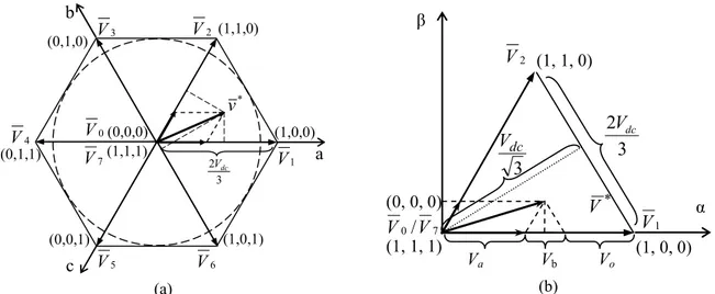
2.3. Space vector representation...46
2.4. Single and double supply...49
2.4.1. Single supply...50
2.4.2. Double supply ...52
3.
Modulation strategies for dual inverter: state of the art ... 55
3.1. Fundamental frequency switching... 56
3.1.1. Space vector control...56
3.1.2. Selective harmonic elimination...57
3.2. Modulation techniques for two-level voltage source inverters... 59
3.2.1. Carrier-based PWM ...59
3.2.2. Space vector PWM ...61
3.2.3. Unified modulation ...66
3.3. PWM control methods ... 67
3.4. PWM methods carrier based... 69
3.4.1. Independent modulation...69
3.4.2. Level-shifted modulation ...70
3.4.3. Phase-shifted modulation...72
3.5. PWM methods space vector ... 73
3.5.1. Composition of switching periods ...73
3.5.2. Full space vector modulation ...76
3.6. PWM methods for single supply ... 77
3.6.1. Scheme with auxiliary switches...78
3.6.2. Average zero-sequence voltage ...80
3.7. PWM techniques for double supply... 82
3.7.1. Control strategies ...82
3.7.2. Separate supplies power balancing ...83
3.8. Summary ... 84
4.
Proposed modulation strategies for dual inverter ... 87
4.1. Composition of switching periods ... 88
4.1.1. Basic composition of two switching periods ...88
4.1.2. Improved composition of two switching periods...91
4.1.3. Asymmetrical carrier-based composition method...92
4.2. Discontinuous carrier-based PWM ... 94
4.2.1. Discontinuous modulation ...94
4.2.2. Asymmetrical slope carriers...95
4.3. Space vector pulse-width modulation... 97
4.3.1. Determination of the switching sequence ...97
4.3.2. Elimination of double instantaneous commutation...101
4.3.3. Implementation ...103
4.4. Summary ... 104
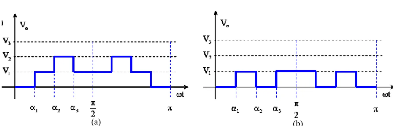
5.1. DC voltage regulation...107
5.1.1. Proposed proportional current reference...109
5.1.2. Proposed Σ-Δ controller...111
5.2. Current control ...112
5.2.1. Survey of current control techniques ...112
5.2.2. Proportional controller ...117
5.3. Synchronization with the grid ...118
5.3.1. Quadrature signals phase-locked loop ...119
5.3.2. Control in dq-domain...121
5.4. Experimental results...122
5.4.1. PLL ...123
5.4.2. Current controller parameters ...123
5.4.3. Voltage controller parameters...125
5.4.4. Simulation of the system...126
5.4.5. Testing of the system ...128
5.5. Summary...130
6.
PV generation with dual inverter ... 133
6.1. Photovoltaic field...133
6.1.1. Panel ratings...133
6.1.2. Series/parallel connection of the modules...136
6.2. Maximum power point tracking...139
6.2.1. Maximum power point tracking state of the art ...140
6.2.2. Dual inverter photovoltaic application...141
6.2.3. Proposed maximum power point tracking algorithm...143
6.3. Experimental results...145
6.4. Summary...148
7.
Conclusion and future work ... 151
7.1. Conclusion ...151
1. Introduction
1.1. An overview of multilevel inverters
The increase of the world energy demand has entailed the investment of huge amounts of re-sources, economical and human, to develop new technologies capable to produce, transmit and convert all needed electric power. In addition, the dependence on fossil fuels and the progressive increase of its cost lead to appearance of new cheaper and cleaner energy resources not related to fossil fuels. In ultimate decades, renewable energy resources have been the focus for researchers, and different families of power converters have been designed to integrate these types of sup-plies into the distribution grid. Beside the generation, electric power transmission needs high-power high-power electronic systems to assure conversion and the energy quality. Static converters such are high-voltage dc (HVDC), static synchronous compensator (STATCOM) and flexible alternating current transmission system (FACTS) are becoming standard part of the high-voltage grid in addition to traditional transformers and power lines. Last but not least, numerous industry applications, such as for example textile and paper industry, steel mills, electric and hybrid elec-tric vehicles, ship propulsion, railway traction, ‘more-elecelec-tric’ aircraft, etc., require utilization of variable speed electric drives. As far as the variable speed operation of electric drives is con-cerned, this is nowadays invariably achieved by supplying the machine, regardless of the type, from a power electronic converter.
Therefore, power electronic converters have the responsibility to carry out these tasks with high efficiency. At each of these stages rapid development of the power electronic lead to im-plementation of new power converter topologies and semiconductor technologies. Furthermore, the progress has been enabled by rapid developments in the areas of control algorithms, power semiconductors and microprocessors/digital signal processors (DSPs) during the last decades. Combining fast-switching power semiconductors with computationally powerful DSPs provides a convenient way to realize the complex control algorithms for power converters, so that excel-lent quality of control is achieved. Modern power semiconductor devices make this design prac-tical for use at medium-voltage level.
A continuous race to develop higher-voltage and higher-current power semiconductors to drive high-power systems still goes on. In this way, the last-generation devices are suitable to support high voltages and currents (around 6.5 kV and 2.5 kA). However, currently there is tough competition between the use of classic power converter topologies using high-voltage semiconductors and new converter topologies using medium-voltage devices. These two con-cepts are shown in Fig. 1, where multilevel converters built using mature medium-power semiconductors are competing with classic power converters using high-power semiconductors that are under continuous development and not mature. Indeed, multilevel converters using more switching components can be both cheaper and more reliable than standard two-level solution
with rare and more expensive components. In addition, multilevel solution requires smaller filter to satisfy power quality requirements, which can be significant item in high-power range. Nowa-days, multilevel converters are a good solution for power applications because they can achieve high power using mature medium-power semiconductor technology [1], [2], covering power range from 1 MW to 30 MW [3].
The maximum power limit of standard three-phase converters is related to the limits of the maximum voltage and current of a switching component. Furthermore, higher is the power of a switch lower is the switching frequency. An initial solution to overcome these limitations was connection of several switches in series or in parallel. The series connection of two or more semiconductor devices faces problems due to the difficulty to synchronize perfectly their com-mutations. In fact, if one component switches off faster than the others it will blow up because it will be subject to the entire voltage drop designed for the series. Instead, parallel connection is slightly less complicated because of the positive resistance coefficient property of MOSFETs and IGBTs with the increment of junction temperature. When a component switches on faster than the others do, it will conduct a current greater than the rated one. In this way, the component increases its junction temperature and its resistance, in this way limiting the current to some ex-tent. This effect makes possible to overcome the problems coming from a delay among gate sig-nals or from differences among real turn on time of the components. Nevertheless, parallel con-nection of the switches has its limits: it requires careful I precise design of the system to achieve almost perfect symmetry of the components, a task more difficult to maintain as their number rises.
Moreover, multilevel converters present several other advantages:
• Generate better output waveforms with a lower dv/dt than the standard converters (power quality).
• Increase the power quality due to the great number of levels of the output voltage: in this way, the AC side filter can be reduced, decreasing its costs and losses (low switching losses). High Power Applications Semiconductors High Power Applications
Classic Two-Level Converters Multilevel Converters
0
NPC capacitorsFlying Cascaded H-bridge
• Can operate with a lower switching frequency than two-level converters, so the electromagnetic emissions they generate are weaker, making less severe to comply with the standards (EMC).
• Can be directly connected to high voltage sources without using transformers; this means a reduction of implementation and costs.
The main disadvantages of this technique are:
• Larger number of semiconductor switches required increasing complexity compared to the two-level solution.
• Capacitor banks or insulated sources are required to create the dc voltage steps.
Multilevel converters are a viable solution to increase the power with a relatively low stress on the components and with simple control systems. The increase of maximum output voltage and number of levels is shown in Fig. 2 for two-, three- and four-level inverter with equal dc voltages applied to three-phase star-connected load. To some extent, the structure was born from the previous idea of series switch connection, with a significant modification that voltages across the switches need to be determined (fixed). This concept can be clearly seen for the simplest di-ode-clamped multilevel inverter shown in Fig. 3(a). Capacitor voltages can be fixed in a simple manner by connection of separate dc sources. If numerous isolated sources are not easily avail-able, the dc bus voltage is split in several equal steps respectively by capacitor banks which need to be held equal by closed-loop control. It should be noted that before the introduction of the multilevel inverters high-power converters were typically realized by current source inverters, increasing the current ratings instead of voltage. This type of inverters are in continuous decline ever since.
The most common multilevel converter topologies are [4]: • Diode clamped (neutral-point clamped),
• Flying capacitor (capacitor-clamped), • Cascaded topology.
In addition, numerous hybrid topologies exist, derived from these basic types by varying or cascading them. In should be emphasized that in general all types of multilevel converters can produce the same voltage output, but with significant difference in number of the switches, their
3 2Vdc 3 4Vdc dc V 2 (a) (b) (c)
briefly overviewed in following section, whereas the cascaded topologies will be treated in more details in the next chapter.
1.1.1. Diode clamped inverters
Proposed almost thirty years ago, this converter is based on a modification of the classic two-level converter topology adding new power semiconductors per phase. The simplest NPC con-verter is shown in Fig. 3(a), implementing three leg voltage levels by doubling the number of switches and adding the same number of diodes to each additional switch. An additional level is clamped through the diodes (clamping diodes) connected to so-called neutral point of the source, as denoted in Fig. 3(a). Using this new topology, each power device has to stand, at the most, half voltage compared with the two-level case with the same dc-link voltage. Therefore, having the same power semiconductors ratings as the two-level case, the output voltage can be doubled. Note that for number of leg voltage levels n higher than three there is no single clamped point, (for even number of levels there is no neutral point at all). Based on the parity of the n converters are divided in neutral point clamped (NPC) for an odd number, and multi-point clamped, when n is even.
The principle of the switching is quite simple: for n-level inverter highest (n-1) adjacent switches need to be turned on together to achieve maximum leg voltage, next (n-1) switches to be turned on for (n-2)-th output level etc, up to the last (n-1) switches, which turned on together give zero leg voltage. There are also limitations: turning on n adjacent switches would lead to shoot-through. This can be illustrated on a three-level and four-level examples (Fig. 3), which are also of the highest practical interest, with the switching combinations given in Tab. 1. There are only three useful combinations for three-level case, whereas the other lead to undefined states. Therefore, this multilevel inverter has no redundant states (i.e. different switching combinations leading to the same output voltage). Similar conclusion can be made from four-level inverter switching states (Tab. 1).
However, four-level inverter has a serious drawback compared to three-level one: additional diodes do not have equal reverse voltage. Indeed, when Ta5 and Ta6 are on, diode Da2 has to
withstand reverse voltage equal to 2Vdc, which is double of the transistors rated voltage. Furthermore, for inverters with higher number of levels this voltage further increases. In addition, switches are not directly clamped to the dc link capacitors by the opposite freewheeling diodes, except for the outmost two, in contrast to two-level inverter. In this way static or stray inductance overvoltage can appear across the switches. These two are the biggest drawbacks of NPC inverters with higher number of levels, because it practically turns back the problem to the initial series connection of switches.
For these reasons, three-level inverter is the most popular within its class. In order to solve these problems for higher number of levels a different diode-clamped topology has been proposed [5]. The structure provides a more direct clamping both diodes and switches to the dc capacitors. An example of four-level inverter is shown in Fig. 4(a). It can be noted that role of the “inner” diodes D2 D3 from Fig. 3(b) is shared between more diodes in Fig. 4(a). This
topology can be also seen as derived from three-level inverter in Fig. 3(a) by adding “nested” clamping diodes instead of “crossed” as in Fig. 3(b).
Taking the same three-level topology as a starting point another type of multi-point clamped inverter can be derived, as shown in Fig. 4(b). This four level inverter using couples
switch-di-Tab. 1. Switching states and leg output voltages for three-level and four-level diode-clamped inverters
State of the switches 3-level
Ta1 Ta2 Ta3 Ta4 Leg voltage
1 1 0 0 Vdc
0 1 1 0 0
Value
0 0 1 1 -Vdc
State of the switches 4-level
Ta1 Ta2 Ta3 Ta4 Ta5 Ta6 Leg voltage 1 1 1 0 0 0 1.5Vdc 0 1 1 1 0 0 0.5Vdc 0 0 1 1 1 0 -0.5Vdc Value 0 0 0 1 1 1 -1.5Vdc
ode instead of using a simple diode to clamp voltages. This type of converter contains the same number of the switches as previously presented diode-clamped counterparts, but requires a more complex control due to the presence of additional controllable switches. However, the modula-tion can be simplified pairing complementary switches as can be seen in Tab. 2. Moreover, the switches in the middle of the leg must carry twice the voltage of the others. The benefits of the structure are lower number of switches in series that conduct and therefore lower losses.
A common drawback for all diode clamped inverters (DCI) is caused by its series connection of controlled switches: the switches closer to the leg output conduct more pulses than those further, e.g. for three-level inverter Ta2 conducts double of Ta1 current. Furthermore, the difference increases with the number of levels. Both drawbacks limit the number of levels in practice to a five [6]. Additionally the structure is not modular; increase in number of levels requires complete reconfiguration instead of simple addition of modules. Nevertheless, NPC is one of the most popular multilevel converters in more conventional high-power ac motor drive applications like conveyors, pumps, fans, and mills, which offer solutions for industries including oil and gas, metals, power, mining, water, marine, and chemistry. Another application of this converter is as high-voltage rectifier for grid-supplied loads [7] or wind turbines, where a back-to-back (active front-end) topology became an industrial standard [8].
1.1.2. Flying capacitor inverters
The flying capacitor (FC) topology is in some way derived from it diode clamped predecessor by the simplification – elimination of the clamping diodes. FC inverter uses additional capacitors oppositely charged to be included in series with dc supply, since after the elimination of the diodes it is not possible to connect leg output directly to the desired dc voltage. These capacitors have the same function of the clamping diodes in diode-clamped converter: they keep constant the voltage drop between the busses to which they are connected. For this reason, they are called clamping capacitors, giving the name to the converter [3]. Another name that can be found in the literature is the nest cell converter [9]. The principle of the switching is similar to the DCI, and will be explained for three-level and four-level examples shown in Fig. 5. However, there is a difference in the principle: clamping capacitors need to be connected in series, and must not be short-circuited by turning on switches connected in parallel. The switching table is given in Tab. 3, showing redundancy for leg output voltage equal to zero which is another difference with respect to DCI. These voltage-level redundancies can be used as extra degrees of freedom for
State of the switches
Ta1 Ta2 Ta3 Ta4 Ta5 Ta6 Ta7 Ta8 Leg voltage 1 1 1 0 0 0 0 1 2Vdc 1 1 0 1 0 0 1 0 Vdc 1 0 1 0 0 1 0 1 0 1 0 0 1 0 1 1 0 0 0 0 1 0 1 1 0 1 -Vdc Value 0 0 0 1 1 1 1 0 -2Vdc
control or optimization purposes. However, the main and most important difference with the NPC topology is that the FC has a modular structure that can be more easily extended to achieve more voltage levels, for this reason sometimes called multicell inverter [6]. This can be easily observed by redrawing the FC as illustrated in Fig. 6(a) showing the unit cell of the inverter. This makes possible a modular approach presented in Fig. 6(b).
The main drawback of the FCI is complex control algorithm and many voltage sensors for high number of capacitor voltages to be controlled. Another problem is capacitors flying connection that requires both initialization and control, which requires the use of the redundant states. The hardware disadvantage is requirement for significant number of capacitors. Since the applications are at lower carrier frequencies the high values of capacitors is the major disadvantage of the FCI [3]. In addition, capacitors are unequally rated, as can be noted in Fig. 5(b), where the outer capacitors need to withstand almost full dc voltage, compared to DCI where all capacitors were equal and relatively small. In addition, the drawback of unequal switch currents common with DCI remained. To conclude, the youngest among the common multilevel configurations (proposed less than twenty years ago), this converter remained in the shadow of the other two competitors.
A generalized structure including in itself both diode-clamped and flying capacitor converters has been found [10]. This generalized clamped inverter has modular structure with the same
Fig. 5. Flying capacitor inverter (a) three-level, (b) four-level.
Tab. 3. Switching states and leg output voltages for three-level flying capacitor inverter
State of the switches 3-level
Ta1 Ta2 Ta3 Ta4 Leg voltage 1 1 0 0 Vdc 1 0 1 0 0 0 1 0 1 0 0 0 1 1 -Vdc Value 0 1 1 0 short-circuit
basic cell as FCI from Fig. 6(a), as can be seen from Fig. 7(a). By omitting some switches (transistors and/or diodes) basic clamped converters can be derived, such is FC shown in Fig. 7(b). In similar manner, both types of the diode clamped inverters (shown in Fig. 3(a) and Fig. 4(a) respectively) can be derived.
1.1.3. Hybrid configurations
The major advantages of the hybrid structure include the fact that it joins the best performance characteristics of two different power converters, and can achieve similar performance to other multilevel VSCs with a reduced number of switches (e.g. 24 for seven-level hybrid VSC as opposed to 36 for diode-clamped, cascaded, capacitor-clamped VSCs). There are three principles how hybrid configurations are derived:
• Combining from three basic multilevel structures (mixed-level hybrid) • Combining different dc supplies (asymmetric hybrid)
• Combining different modulation principles and usually more than one of the principles is used.
(a)
(b) Fig. 6. Modularity of flying capacitor structure (a) unit cell, (b) converter.
(a) (b)
A typical example for the third method is combination of high-voltage (high-power) and low-voltage (low-power), as illustrated in Fig. 8. In terms of operation, the hybrid converter uses the HV stage to achieve the bulk power transfer and the LV stage as a means to improve the spectral performance of the overall converter. This enables a HV stage to be made of HV blocking components but not necessarily fast switching ratings (e.g. thyristors), while the LV stage is constructed using devices that have fast switching characteristics but not necessarily high-voltage blocking characteristics (e.g. IGBT). In mixed-level hybrid multilevel cells converter, the H-bridge cells of cascaded leg are substituted by diode-clamped or flying-capacitor. Mixed-level hybrid multilevel cells converter is well suited for high-voltage high-power applications because of the reduction of required insulated sources in the respect of a cascade H-bridge with the same number of output levels. Since most of the hybrid configurations include some way of cascaded connection it will be elaborated in more details in the next chapter.
Drawbacks of the hybrid solutions the converter control is more complex than standard. Fur-thermore, in case of grid supply different dc sources require additional transformer windings and rectifiers. Another problem that must be addressed for the hybrid converter is that the HV stage will supply more power than the load requires in the middle ranges of the modulation index. Un-der these operating conditions, the LV stage will be required to operate in a rectification mode, which means that the dc link must be capable of a bidirectional power flow. This necessitates the use of a PWM rectifier on the front end and further complicates the system. However, at medium and high power levels advantages of reduced switch count still make it attractive.
Combinations of the diode-clamped and cascade converters are also possible. Figure 9(a) shows one implementation that combines a three-level NPC with a single-cascade two-level transistor H-bridge (subinverter) in series with each phase. In this case, six levels can be obtained. To keep the power part simple and the efficiency high, the subinverters have no feeding from the net and can only supply reactive power [11]. Another topology is a cascaded-transformer inverter shown in Fig. 9(b), that adds up output voltage on the expense of the transformer windings. In this way, the number of switching devices and other components of conventional multilevel inverters such as diode-clamped, flying capacitors, and cascaded full-bridge cells can be saved.
(a) (b)
1.2. Photovoltaic conversion
1.2.1. Extraterrestrial solar energy
The Sun is made up of about 80% hydrogen, 20% helium and only 0.1% other elements. Its radiant power comes from nuclear fusion processes, during which the Sun loses 4.3 million tones of mass each second, to be converted into radiant energy. Each square meter of the Sun’s surface emits a radiant power of 63 MW, which means that just a fifth of a square kilometer emits an amount of energy equal to the global primary energy demand on Earth. Fortunately, solar irradiance decreases with the square of the distance to the Sun, so only a small part of this energy reaches the Earth’s surface. Applying the Stefan-Boltzmann’s law to the Sun and Earth the radiant flux, received from the Sun outside the Earth’s atmosphere can be calculated as 1360 W/m2 [12]. Since the distance of the Earth to the Sun changes during the year, solar irradiance outside the earth’s atmosphere also varies between 1325 W/m² and 1420 W/m². The annual mean solar irradiance is known as the solar constant and is 1367 W/m². The radiation intensity outside the Earth’s atmosphere according to the solar constant is called the extraterrestrial radiation. The first practical conversion of solar to electric energy was to power orbiting satellites and other spacecraft, but today the majority of photovoltaic modules are used for grid connected power generation.
Only a surface that is perpendicular to the incoming sun’s rays receives this level of irradiance. Outside the atmosphere, and therefore not subject to its influence, solar irradiance has only a direct component – all solar radiation is virtually parallel. This irradiance is also called direct normal or beam irradiance Ebeam. Under these conditions, a surface that is oriented parallel to the sun’s rays receives no irradiance. The specific direct solar irradiance Edir that reaches an inclined surface is lower depending on the cosine of the angle of incidence φ:
ϕ
cos
beam
dir E
E = (1)
This is illustrated in Fig. 10(a), where can be seen that for with increase of the angle φ the same radiation power covers larger area, thus decreasing the irradiance as per area value.
(a)
(b)
Fig. 9. Examples of cascaded hybrid inverters: (a) diode-clamped and cascade converter combination (b) cascaded multitransformer inverter.
The Sun’s outer surface, namely photosphere, has an effective blackbody temperature of approx. 6000 K. Viewed from the Earth, the radiation emitted from the Sun appears to be essentially equivalent to that emitted from a 6000 K blackbody at, with wavelength maximum around 500 nm - yellow color. The total amount of radiation present, at all frequencies is shown in Fig. 10(b) for radiation incident on a surface, called spectral irradiance, and has SI units W/m3, or commonly W·m−2·nm−1.
1.2.2. Insolation quantities and measurement
Various different terms are used when dealing with solar radiation, often incorrectly even by some solar specialists [13].
• The total specific radiant power, or radiant flux, per area that reaches a surface is called irradiance. Irradiance is measured in W/m² and has the symbol E.
• When integrating the irradiance over a certain period it becomes solar irradiation. Irradiation is measured in either J/m² or Wh/m², and represented by the symbol H. Since the variation of annual irradiations from year to year can be well over 20 %, a measurement period should cover at least 7–10 years. Insolation (incident solar radiation) is a measure of solar radiation energy received on a given surface area in a given time. It is commonly expressed as average irradiance in watts per square meter W/m2 or kilowatt-hours per square meter per day kWh/(m2·day) (or hours/day).
• For daylight purposes, only the visible part of the sunlight is considered. The analogous quantity to the irradiance for visible light is the illuminance. This uses the unit lm/m² (lu-men/m²) or lx (lux). Direct sunlight has a luminous efficacy of about 93 lm/W of radiant flux, which includes infrared, visible, and ultraviolet light. Bright sunlight provides illumi-nance of approximately 100.000 lux or lumens per square meter at the Earth's surface. • Direct insolation is the solar irradiance measured at a given location on Earth with a
surface element perpendicular to the Sun's rays, excluding diffuse insolation (the solar radiation that is scattered or reflected by atmospheric components in the sky).
• Diffuse insolation is the solar radiation that is scattered or reflected by atmospheric components (clouds, for example) to the Earth's surface.
(a) (b) Fig. 10. Earth’s atmosphere effect on the solar radiation (a) attenuation (b) spectral distribution.
Measurement of the solar irradiance is a quite demanding task, dust on the sensors, inaccurate trackers or dirt can reduce the measurement quality significantly. Today common sensors can be classified as:
• Low-cost pyranometers, Fig. 11(a), use silicon sensors with a small photovoltaic cell that generates an electrical current that is nearly proportional to the global solar irradiance. A pyranometer measures the global irradiance and typically does not require any power to operate. However, these sensors measure only part of the solar spectrum – they cannot sense infrared light. The annual accuracy of these sensors is limited because the spectrum changes with the air mass. In the ideal case, it can be in the range of 5 %.
• Pyranometers that are more precise use a black receiver plate that is mounted below a double glass dome, Fig. 11(b), and the plate heats up depending on the incoming irradiance. A thermocouple converts the heat difference between the plate and its surroundings into a voltage signal that is proportional to the irradiance. These sensors can obtain annual accuracies well above 3%. For irradiance measurement by definition is required that the response to “beam” radiation varies with the cosine of the angle of incidence. This means full response when the solar radiation hits the sensor perpendicularly (normal to the surface, sun at zenith, 0 degrees angle of incidence), zero response when the sun is at the horizon (90 degrees angle of incidence, 90 degrees zenith angle), and 0.5 at 60 degrees angle of incidence. It follows from the definition that a
(a) (b)
Fig. 11. Insolation sensors (a) Solarc “Mac-Solar E“ meter, (b) Hukseflux SR11 first class pyranometer.
(a) (b) Fig. 12. Irradiance sensors (a) two-axis tracked pyrheliometer for direct normal irradiance measurements (b) with
pyranometer should have a so-called “directional response” or “cosine response” that is close to the ideal cosine characteristic.
• To measure the direct normal or beam irradiance, the sensor is mounted inside the end of an absorber tube (this tube keeps the diffuse irradiance away). This so-called pyrheliometer has to be mounted on a two-axis tracker that follows the sun very accurately, Fig. 12(a). If a shading ball, or shading ring, permanently shades a pyranometer, it measures the diffuse irradiance since direct irradiance is kept away, Fig. 12(b).
1.2.3. Solar energy on the Earth
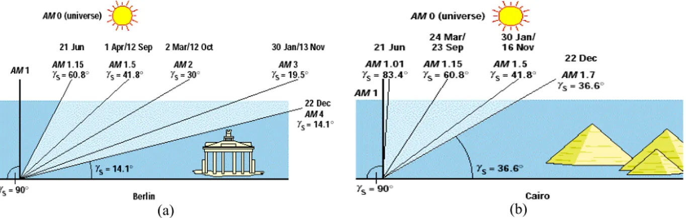
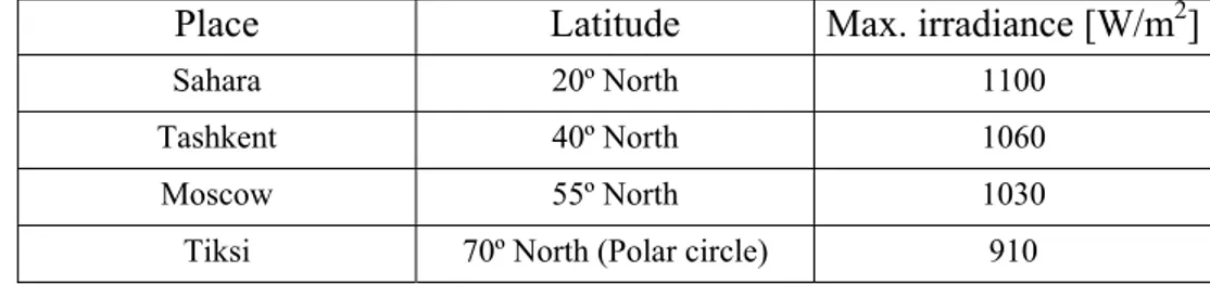
However, the almost constant extraterrestrial radiation is highly variable on the Earth surface due to the attenuation such as reflection, scattering (reflection in many directions) and absorption in the Earth atmosphere, which means that only some part of incident radiation becomes transmitted. A well-known example is ultraviolet part of the solar energy absorbed by ozone in the stratosphere. Furthermore, there is additional attenuation of the clear sky is determined by the length of the atmospheric path traversed by sunlight, which refers to the so-called relative Airmass (AM). The solar radiation is reflected and scattered primarily by clouds (moisture and ice particles), particulate matter (dust, smoke, haze and smog) and various gases. Airmass represents the strength (mass) of the atmosphere, and can be approximated by (1) with the Sun at the angle to overhead, as illustrated in Fig. 10(a).
Air Mass =1/cosϕ (2)
Spectrum AM 0 denotes extraterrestrial radiation whereas AM 1.5 approximately represents solar noon near the spring and autumn equinoxes at the 45º latitude with surface of the cell perpendicular to radiation and is used for standard testing (Fig. 13).
With the Sun overhead at noon, the sky appears white because little scattering occurs at the minimum atmospheric path length. At sunrise and sunset, however, the solar disc appears red because of the increased atmospheric path associated with relatively high scattering of the short wavelength blues and greens. As a result, the irradiation falling to the optimally set surface is at a see level at midday amounts of 1000 W/m2 when the sky is cloudless. Of this energy approximately 527 W is infrared, 445 W is visible, and 32 W is ultraviolet part of the spectrum. With altitude, the maximum values of radiation increases due to the decrease of the optical thickness of the atmosphere: for every added 100 m value of radiation in the troposphere
(a) (b)
increases by 0.007-0.014 kW/m2. Maximum values of radiation recorded in the mountains reach 1190 W/m2.
There are three major sources of irradiation variability:
• Change in Earth's atmosphere regarding the movement of the clouds, particulate matter (dust, smoke, haze and smog) and various gases. As a consequence, the maximum irradiation is attenuated up to only 150 W/m2 in an overcast dull day.
• Change of Sun tilt angle due to the Earth rotation. The radiation intensity on the Earth’s surface changes continually during a day even if the sky is clear. Less radiation is available early in the morning or late in the afternoon, when the rays make a longer path through the atmosphere and therefore more attenuation than at midday, as illustrated in Fig. 14 for different time of the day.
• Change of the inclination of the Sun's trajectory in the sky (as seen by an observer on Earth's surface) due to the axial tilt of the Earth (often known as the obliquity of the ecliptic), varies over the course of the year (Fig. 13). For the northern hemisphere the minimum values of insolation occur in December, and the maximum at spring when the air contains less condensation products and dust then in summer. Although the difference by comparing Fig. 14(a) and (b) is significant, it can be seen that the difference between seasonal maximum irradiation in temperate latitudes is not so drastic. However, it increases towards the poles where winter irradiation becomes zero.
Surprisingly, the maximum direct irradiance little increase with decreasing of latitude, despite the increase in the height of the Sun. This is because of increasing moisture and dust content in air in southern latitudes. Therefore, at the equator, the maximum values are slightly greater than the maximum in temperate latitudes. As an illustration, the maximum direct irradiance at the following places in W/m2 is given in Tab. 4 [14]. Experimental results are very prone to the influence of this change. Therefore they should be conducted close to the sun highest position, which is usually around noon in "winter season" (from autumn to spring, no daylight saving time), and around 1 PM in the remaining part of the year (from spring to autumn, daylight saving time). Around this time, the derivative of the cosine function is minimal, so the change of the irradiation is as small as possible. In contrary, in early morning (late afternoon) changes are so quick that on a clear sky almost every few minutes power increase (decrease).
(a) (b)
1.2.4. Photovoltaic cells
Photovoltaic cell provides direct conversion of sunlight to electricity. It is actually a p-n junction, like ordinary diode; however, its construction is adapted to maximum utilization of solar radiation. The principle is based on the interaction between incident photons and silicon (or other element) electrons, which generates an electron-hole pair, if the photon energy is higher than the silicon band gap value. However, much of the solar radiation reaching the Earth is composed of photons with energies greater than the band gap of silicon. These higher energy photons will be absorbed by the solar cell, but the difference in energy between these photons and the silicon band gap is converted into heat via lattice vibrations rather than into usable electrical energy. This specific portion of the radiant energy cannot be used, because the light quanta (photons) do not have enough energy to "activate" the charge carriers. This leads to a theoretical maximum level of efficiency, e.g. approximately 28 % for crystal silicon (Fig. 15).
Numerous efforts were done to determine equivalent circuit applicable to all conditions. A typical circuit is shown in Fig. 16(a), representing the cell as an antiparallel connection of the non-ideal current source and a diode, with additional resistances in series Rs and parallel Rsh [12]. For low values of the cell output voltage V (corresponding to lower load resistance) the diode voltage is bellow its threshold and almost all source light-generated current IL is obtained as the output current I. To a very good approximation, the cell “light” current IL is directly proportional to the cell irradiance. As the output voltage increases, the diode is surpassing the threshold and conducting bigger portion of the source current, up to the no-load condition when all the current
IL is overtaken by the diode. The I-V characteristic of a typical PV cell is given in Fig. 16(b) between Isc and Voc points. Note that the amounts of current and voltage available from the cell
Tab. 4. The maximum direct irradiance for places with the different latitude.
Place Latitude Max. irradiance [W/m2]
Sahara 20º North 1100
Tashkent 40º North 1060
Moscow 55º North 1030
Tiksi 70º North (Polar circle) 910
Material Conversion efficiency in lab [%] Conversion efficiency in production [%] Monocrystalline Silicon 24 14 - 17 Polycrystalline Silicon 18 13 - 15 Amorphous Silicon 13 5 -7 (a) (b)
depend upon the cell illumination level. In the ideal case, the I-V characteristic equation is ) 1 ( − − = kT qV o L I e I I (3)
where IL is the component of cell current due to photons, q = 1.6x10⁻¹⁹ C, k = 1.38·10–23 J/K and
T is the cell temperature in Kelvin. While the I-V characteristics of actual PV cells differ
somewhat from this ideal version, (3) provides a means of determining the ideal performance limits of PV cells. To determine the open circuit voltage of the cell, the cell current is set to zero and (3) is solved for Voc, yielding the result:
o l o o l OC I I q kT I I I q kT V = ln + ≈ ln (4)
since normally I >> Io. For example, if the ratio of photocurrent to reverse saturation current is 1010, using a thermal voltage (kT/q) of 26 mV, yields Voc = 0.6 V. Note that the open circuit voltage is only logarithmically dependent on the cell illumination, while the short circuit current is directly proportional to cell illumination.
As a result, there are two different zones, so called "voltage source" and "current source" zone, separated by buffer area conditionally called MPP zone, denoted in Fig. 17(a). Zones are
(a) (b) Fig. 16. PV cell (a) equivalent circuit, (b) V-I diagram.
MPP V I,P I(V) P(V) Voltage generator zone Current generator zone (a) (b) Fig. 17. Cell I-V characteristic (a) Two different behaviors of PV cell (panel) separated by MPP zone, (b) irradiation
also called "low impedance" and "high impedance" zone, since dv/di is small in the first one and very high in the second (di/dv→0) (but always negative). Between the two extreme working points with zero output power (short-circuit and no-load), there is a point with the maximum output power, which is often of the outmost interest. The area around that point is highly non-linear, also known as “the knee”. Due to extremely low output voltage, approximately equal to standard diode threshold voltage of 0.6-0.7 V, cells are always connected in series (string) forming a PV module. The data for a different irradiance levels are given for Shell Solar SP150 module in Fig. 17(b), which will be used for experiments in this work.
1.3. Research objectives and originality of the work
The thesis analyzes a multilevel converter from its structure over modulation up to application in a grid-connected photovoltaic system. The principal objectives of the work were:
1. To carry out a comprehensive modeling of three-phase multilevel voltage source inverters, with emphasis on cascaded and dual VSIs.
2. To investigate characteristics of continuous carrier-based and space vector based pulse width modulators for three-phase dual two-level VSIs, operating in the linear modulation region.
3. To examine advantages and shortcomings of both approaches defined above, and establish bi-directional link between carrier-based and space vector pulse width modulators for dual two-level VSIs.
4. To develop PWM schemes for dual two-level VSIs (using carrier-based and space vector approach), which are able to produce proper multilevel output voltage applicable to control of three-phase loads and connection to the grid.
5. To develop PWM schemes for dual two-level VSIs (using carrier-based and space vector approach), which are able to control the dc-link voltage in accordance with the dual inverter application.
6. To explore and develop analytical tools for characterization of the dc-link voltage control methods for dual two-level inverter.
7. To design and build dual two-level VSI with accompanying DSP control system for the purpose of experimental verification of results obtained by theoretical and simulation studies.
8. To design and build photovoltaic generation system capable of injecting power into the grid and tracking operating point of the maximum power under different environmental conditions.
By achieving the objectives listed above, a significant body of new knowledge has been produced. This is partially evidenced by the already published research papers that have resulted from the thesis, which can be found within cited references. Chapters four to six contain the original results from the research and therefore represent the main contributions of this work.
1.4. Organization of the thesis
Corresponding to research objectives, the thesis is organized in four major parts that are background, modulation, application and conclusions. More detailed, structure consists of eight chapters, followed by three appendices.
Chapter 1 contains an overview of multilevel power converters. A multilevel topology based on the use of today’s mature technology supplied from multiple dc sources is identified as a potentially viable solution for application in the high-power conversion systems. Existing three-phase multilevel power converters are introduced advantages and drawbacks briefly surveyed. Of today’s three most exploited configurations, two of them are addressed here, since they are not of the principle interest. A brief introduction of the photovoltaic conversion principles in terrestrial applications is given, with the emphasis on the electrical characteristics of the photovoltaic converter as an electric source. The need for the research conducted within the scope of this thesis is thus established and objectives of the research are finally set forth.
The basic characteristics of the dual two-level inverter VSIs as a multilevel converter of the principle interest are addressed in Chapter 2. First, the configuration is introduced within broader class of cascaded multilevel inverters, showing the performances of the dual inverter with comparison to possible alternatives. The voltage space vectors concept is applied in order to determine the output voltage, with the mapping of switching combinations and the classification of the obtained vectors is given. This foundation is necessary for development of the PWM methods based on the space vector approach. Additionally, modeling aspects of a multi-leg VSI are covered, emphasizing similarities with a three-phase VSI that are used later on for development of the PWM scheme.
The third chapter presents a literature survey in the area of PWM techniques for dual two-level inverter, starting from the basic fundamental frequency methods up to newest space-vector techniques. Due to the differences in dual inverters with double and single dc supply, and having in mind that the emphasis in this thesis is on double-supplied dual inverter, PWM methods applicable to these two configurations are reviewed separately. Additionally, the concept of the power balance of the two sources has been introduced. The chapter also includes a survey of the basic two-level inverter techniques that are the cornerstone for the modulation of dual inverter.
Chapter four deals with development of modulation schemes with power sharing capability for a dual VSI. They use a degree of freedom present at the double-supplied structure to control the two dc powers. Three modulation algorithms are developed based on the utilization of different approaches. It is demonstrated at first that simple extension of well-known principles of a three-phase PWM provides relatively simple yet satisfactorily solution for the dual inverter. Therefore, two CBPWM schemes are introduced, based on the use of discontinuous modulation and composition of the switching periods that are able to generate output voltage without the double simultaneous commutations. Experimental results that are collected from a developed converter prototype show excellent match with predicted theoretical results obtained by means of theoretical analysis and simulations.
A particular dual inverter application as a grid connection converter is treated in Chapter 5. The major issues of such configuration are formulated in the following order: dc-link voltage regulation, current control and synchronization with the grid. Regarding the voltage regulation a two different controllers were proposed. For a current control, a simple proportional controller has been shown as satisfactorily choice with respect to its simplicity. Similarly, a simply yet efficient synchronization solution was implemented. All these aspects were tested separately, provided the possibility to be tuned separately. Finally, a performance of the whole system has been evaluated on the experimental prototype.
The photovoltaic generation application of the dual inverter is presented in Chapter 6. First, a survey on the photovoltaic fields as a source has been presented with practical aspects of their configuration and performance. Another unavoidable aspect of the PV generation is maximum power point tracking that has been briefly surveyed. A new method particularly suitable for the dual inverter configuration has been presented with both the simulation and experimental results obtained. Experimental results are presented, confirming theoretical findings.
Chapter 7 provides conclusions and a summary of the thesis, highlighting the most important findings from each chapter. Guidelines for future research are also given. References are listed at the end of each chapter. The numbered structures (sections, equations, figures, tables, reference) are referred inside the same chapter with ordinal number only (e.g. Fig. 15), and outside its chapter with the leading number of the chapter (e.g. Fig 2.15 denotes Fig. 15 in the second chapter).
References
[1] J. Rodriguez, J.-S. Lai, and F.Z. Peng, “Multilevel inverters: A survey of topologies, controls, and applications,” IEEE Trans. Ind. Electron., vol. 49, no. 4, pp. 724–738, Aug. 2002.
[2] L. Franquelo, J. Rodriguez, J. Leon, S. Kouro, R. Portillo, and M. Prats, “The Age of Multilevel Converters Arrives,” IEEE Ind. Electron. Mag., vol. 2, no. 2, pp. 28-39, June 2008.
[3] J. Rodriguez, L. Franquelo, S. Kouro, J. Leon, R. Portillo, M. Prats, and M. Perez, “Multilevel Converters: An Enabling Technology for High-Power Applications,” Proc. IEEE, pp. 1786-1817, vol. 97, no. 11, Nov. 2009.
[4] J. Rodriguez, S. Bernet, Bin Wu, J.O. Pontt, and S. Kouro, “Multilevel Voltage-Source-Converter Topologies for Industrial Medium-Voltage Drives,” IEEE Trans. on Ind. Electron., vol. 54, no. 6, pp. 2930-2945, Dec 2007.
[5] X. Yuan and I. Barbi, “Fundamentals of a new diode clamping multilevel inverter,” IEEE Trans.
Power Electron., vol. 15, no. 4, pp. 711–718, July 2000.
[6] M. Hagiwara, H.Akagi, “Control and Experiment of Pulsewidth-Modulated Modular Multilevel Converters,” IEEE Trans. Power Electron., pp. 1737-1746, vol. 24, no. 7, July 2009.
[7] J. Rodrıguez, J. Pontt, G. Alzamora, N. Becker, O. Einenkel, and A. Weinstein, “Novel 20 MW downhill conveyor system using three-level converters,” IEEE Trans. Ind. Electron., vol. 49, pp. 1093–1100, Oct. 2002.
[8] E. J. Bueno, S. Cóbreces, F. J. Rodríguez, A. Hernández, and F. Espinosa, “Design of a back-to-back NPC converter interface for wind turbines with squirrel-cage induction generator,” IEEE Trans. Energy Convers., vol. 23, no. 3, pp. 932–945, Sep. 2008.
[9] D. Soto and T. Green, “A comparison of high-power converter topologies for the implementation of FACTS controllers,” IEEE Trans. Ind. Electron., vol. 49, no. 5, pp. 1072–1080, Oct. 2002.
Ind. Applicat., vol. 37, pp. 611–618, Mar./Apr. 2001.
[11] M. Veenstra and A. Rufer, “Control of a hybrid asymmetric multilevel inverter for competitive medium-voltage industrial drives,” IEEE Trans. Ind. Appl., vol. 41, no. 2, pp. 655–664, Mar./Apr. 2005.
[12] F. Kininger, "Photovoltaic Systems Technology (script)", University of Kassel, Germany, 2003. [13] V. Quaschning “Technology fundamentals - The Sun as an energy resource,” Renewable Energy
World, vol. 6, no. 5, pp. 90-93, 2003.
[14] N. V. Gusakova “Geography (script in Russian),” http://gusakova.ru/uchebnaya-rabota/nauki-o-zemle.html.
2. Dual inverter configuration
Cascaded converter, together with the described diode clamped and capacitor clamped converters, makes the three most common types of present multilevel topologies [1], [2]. In fact, the series H-bridge design was a forerunner of the whole multilevel family, proposed more than 30 years ago [3]. It still receives large attention among these topologies, due to the simplicity of the power stage not requiring additional components such as diodes and capacitors. As cascaded inverters here is considered broader group of converters having a common “open-end” load connection, i.e. both terminals of the load are connected to the converter. This is illustrated in Fig. 1 by showing single-phase inverters: half-bridge with center tap and full-bridge, both representing the cascaded principle. The main cascaded multilevel inverter configurations are
• cascaded H bridge inverters, • cascaded three-phase inverters, • dual two-level inverters,
and they will be described in the following sections with the emphasis on the last one. This chapter mostly discusses the topology issues, whereas the modulation and control topics are to be addressed in the chapters to come.
The complexity of both leg hardware and control algorithm sharply increases with the number of levels, as was presented in the previous chapter. This drawback lead to a development of the cascaded topology, providing the same number of output voltage levels using two yet simpler multilevel inverters instead of one complex inverter with large number of leg levels. Considering two n2-level inverters connected "in opposition" at two ends of the load, it will be shown that the
obtained structure can produce p2 = 8n2-7 different phase voltage levels of output voltage.
Simultaneously, three-phase inverter consisting of n1-level legs provides p1 = 4n1-3 different
phase voltage levels (including zero) for a star-connected load. Therefore, for n1 less than n2 the
same multilevel output number of levels p2 = p1 can be reached. Moreover, having two inverters
with an appropriated control strategy it is possible to bypass the faulty module without stopping the load, bringing an almost continuous overall availability [4], [5].
(a) (b)
2.1. An overview of cascaded multilevel inverters
2.1.1. Cascaded H-bridge
The idea to cascade (connect in series) single-phase full-bridges was the most natural solution and the first proposed one [3]. Indeed, it is a literal realization of the multilevel principle: each switch works inside its on “module” (here H-bridge), contributing to the total output under limited reverse voltage. The principle can be easily understood with reference to Fig. 2(a) where each H-bridge forms a phase leg for a three-level inverter with the levels +Vdc, 0 and –Vdc. The number l of “leg” output voltage levels for N such cascaded converters become:
1
2 +
= N
l , (1)
from -NVdc to NVdc and including zero voltage. It can be noted that the number of switching levels is always odd (unlike diode-clamped), since inserting additional H-bridge to each phase leg adds two new levels. For a star-connected load it can be shown that these l leg levels will produce p output voltage levels where
3 4 1 ) 1 ( 2 2⋅ − + = − = l l p , (2)
An important advantage of the converter is modularity that can be clearly noted comparing Figs. 2(a) and 2(b).
The dc link supply for each full-bridge converter element must be provided separately, and this is typically achieved using diode rectifiers fed from isolated secondary windings of a three-phase transformer Fig. 3(a). It can be shown that by progressive three-phase shifting of the three-three-phase secondary windings significant harmonic cancellation of the transformer input current can be achieved. However, for single-phase rectifiers this task is more complex [6], since they require connection in groups of three. Another possible solution is in photovoltaic applications [7], [8] as
shown in Fig. 3(b); however, it is highly impractical to have such a large number of connection cables. A particularly convenient application is STATCOM and active power filters, where injection of active power is not required, so the dc voltages can be floating and adjusted to the reference by the control strategy.
In contrast to the diode-clamped and flying-capacitor inverters, where individual phase legs must be modulated by a central controller, an advantage of the cascaded structure of the full-bridge inverters is independence of each other, only the synchronization of reference and carrier waveforms for different phase legs is required. This makes for a simpler controller structure than for either of the two previously discussed topologies. On the other hand, the price is paid by higher number and larger values of the capacitors required since the power flow for each source possess a strong oscillatory component due to its single-phase configuration. Additional advantage is a possibility to load equally all switches of the converter, in contrast to previous two configurations described in Chapter 1. Last but not least, an significant difference is an intrinsic balancing of the capacitor voltages done by the each dc source. This is not the case for the diode-clamped or capacitor diode-clamped inverters where dc link capacitors can be over or undercharged depending of the average current [9].
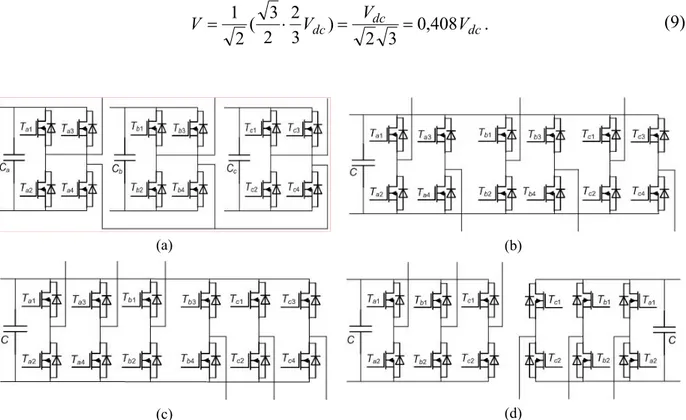
Many of the hybrid multilevel inverters employ H-bridges, as introduced in the paragraph 1.1.3. The topology shown in Fig. 4(a), with a two-level or NPC converter in series with a floating single-phase inverter floating dc-sources [10], offers an optimum tradeoff between output quality, reliability and efficiency. Recently, the use of a multilevel dc-link voltage has been studied in order to increase the number of total output voltage levels using only a few single-phase inverters. The topology is based on a variable dc-link which could have from zero to several voltage levels, then a single-phase full bridge (SPFB) inverter could applies this voltage or its negative [11]. In described configuration, each cascaded inverter cell had the same dc-link voltage value and contributed equally to the total output voltage.
Furthermore, by choosing different dc-link voltages for given number of cells it is possible to increase the number of output voltage levels. This method is called asymmetric cascaded inverter in the literature, and requires binary (power of two) or trinary (power of three) relationship
(a) (b) Fig. 3. Power supply for cascaded H-bridge with (a) grid supply, (b) PV supply.
among the dc-link voltages to provide equal steps of output voltage waveform [10]. By sum\difference of binary potentials can be reached all numbers up to next potential since
1 2 1 ... 2 2N−1+ N−2+ + = N − , (3)
so all natural numbers are covered even with redundancy (e.g. 22 = 23 - 22). In analogous manner can be covered all natural number within interval by sum\difference of potentials of three, but there is no redundancy since the sum reaches exactly up to the “complement of the sum”:
2 1 3 3 2 1 3 1 ... 3 3N−1+ N−2+ + = N − = N − N + (4)
The number of leg voltages levels for N such “binary” inverters will be
1 2 1 ) 1 ... 2 2 ( 2⋅ 1+ 2+ + + = 1− = N− N− N+ l , (5)
since the maximum leg voltage is achieved by the sum of all cell voltages. Analogously
N N N p 1 3 1 3 1 3 2 1 ) 3 ... 3 1 ( 2 1 + = − − = + + + + ⋅ = − , (6)
It can be easily seen that for n higher than three geometrical progressions nN increase too fast and cannot be “reached” by the sum of its previous members.
2.1.2. Cascaded two-level inverter
Instead of cascading H-bridges, it is possible to apply similar idea to two-level inverters, as was proposed in [12]. The obtained structure is depicted in Fig. 5(a), consisting of one standard two-level inverter (ABC) and another slightly modified (DEF, positive dc busbar removed). The structure provides three-level output by simple switching of upper, middle and lower switches, as stated in Tab. 1. The simple and scalable structure for arbitrary number of levels is the main advantage of the proposed topology. The biggest drawback of the scheme is that the lowest switches (Ta4, Tb4, and Tc4 in Fig. 5(a), belonging to the inverter with non-standard layout) have
(a) (b) Fig. 4. Hybrid cascaded topologies with (a) floating dc-link, (b) variable multilevel dc-link voltage diode/capacitor
to withstand the whole dc voltage (i.e. 2Vdc). Another drawback common for clamped inverters is the asymmetry of the inner and outer switches conducting currents.
The Authors [13] applied cascaded two-level inverter in a more complex topology presented in Fig. 5(b). In order to be distinguished from cascaded inverters this kind of structure with two converters connected “in opposition” between an open-winding load will be further called dual inverter. The open winding load is standard three-phase load with six available terminals, in contrast to usual delta and star connections with three (eventually four) output terminals. In this case, the dual inverter is both hybrid and asymmetrical: not only are that two inverters with different number of levels, but also with different dc voltages in ratio 4:1. This is in concordance with the analysis in Subsection 1, since three level inverter provides 4:2 ratio, therefore all steps from Vdc to 5Vdc are obtainable. As a result, the dual inverter is equivalent to six-level converter, therefore increasing the number of leg voltages more than a simple sum 3+2.
2.1.3. Dual inverter structure
Considering dual inverter formed by two identical inverters with l leg voltage levels and using (2) gives the number of the different output voltage levels d (including zero level):
7 8 1 ) 3 4 ( 2 − − = − = n n d . (7)
The two inverters are connected "in opposition" at two ends of the load in order to obtain output voltage as a difference of inverter's leg potentials as shown in Fig. 5(b). The result, when compared to (2) shows that in order to reach given number of output voltage levels it is more convenient to apply two simpler n-level inverters in dual configuration that one large l-level
Fig. 5. Cascaded three-phase three-level inverter: (a) converter, (b) five-level application.
Tab. 1. Switching states and leg output voltages for three-level cascaded inverter.
State of the switches 3-level
Ta1 Ta2 Ta3 Ta4 Leg voltage
1 0 1 0 Vdc
0 1 1 0 0
Value
sharply increases with the number of levels. Comparing (7) with (2) gives
n n
l =2 −1>> . (8)
which is significant reduction compared to n.
A particularly convenient case is obtained for n equal two, which gives multilevel output equivalent to three-level inverter by using standard readily available two-level inverters, avoiding multilevel structure. A possible development path for this solution is illustrated in Fig. 6, starting from the simplest cascaded H-bridge (a), over “double inverter” (b) towards dual two-level inverters with common (c) and isolated (d) dc-supplies. It means that the converter can be considered as derived from the cascaded H-bridge from a structural point of view.
Historically, dual inverter was proposed twenty years ago for high-power drive application [14]. Curiously, the authors did not entered into details of the new topology, paying more attention to the direct-torque control being a pioneering technique at the time. Few years later, a first open-loop modulation technique was presented, and the equivalence with the three-level inverters output was established [15]. However, a whole decade passed before a comprehensive analysis of dual inverter and its counterparts came out [16]. It is worth nothing that no immediate terminology agreement has been set: the inventors called it “dual three-phase inverter”, whereas [16] and [17] diverted from this terminology by using term “cascaded”, which actually corresponds to others topologies as previously explained.
A. Comparison between dual and standard two-level
The first justification of the dual inverter topology comes in comparison with standard two-level inverter [18]. The standard inverter topology (Fig. 7) for a given dc-bus voltage Vdc can produce a phase-to-star-point RMS voltage:
dc dc dc V V V V 0,408 3 2 ) 3 2 2 3 ( 2 1 ⋅ = = = . (9) (a) (b) (c) (d)
Fig. 6. “Evolution” from cascaded to dual inverter (a) cascaded H-bridge with a star connection and 3 insulated dc supply, (b) cascaded H-bridge with open-end winding and single dc supply, (c) simple redraw equivalent to point b, (d) proposed dual-inverter configuration obtained from point c (or b) by splitting the dc supply.
while the switches rated reverse voltage has to be:
dc
sw V
V = . (10)
Similarly, if inverter output current is equal to RMS value I, the current rating of the switch should be the peak value:
I
Isw = 2 . (11) The cost of the switches for the converter is not determined only by their number, but also by their voltage and current ratings determining the power level. Switch utility ratio [19] is a quantitative factor of converters switches utilization obtained as a ratio between converter output power Sc and sum of switches power:
= ⋅ ⋅ ⋅ = = ⋅ = ph dc dc sw sw sw sw c I V I V I V VI I V N S SUR 2 6 408 . 0 3 6 3 0.144. (12)
A similar switching factor is defined in [20]. Here should be noted that switches peak current cannot be provided continuously, therefore the proper factor should take into account continuous current rating: = ⋅ ⋅ = = ⋅ = I V I V I V VI I V N S SUR dc dc sw sw sw sw c 6 408 . 0 3 6 3 0.204. (13)
However, the difference is only in absolute values, the relations remain the same as if peak current would be considered. Moreover, due to the physical reasons switches peak and continuous current ratings are usually proportional.
In case of dual inverter feed by two sources with equal voltage Vdc each, the calculations made analogously manner show:
= ⋅ ⋅ ⋅ ⋅ = ⋅ = ⋅ = I V I V I V VI I V N S SUR dc dc sw sw sw sw c 12 2 408 . 0 3 12 3 0.204. (14)
The same conclusion is obtained by using other indicators in [16] One can observe that dual structure possesses no advantage in comparison to standard inverter in terms of the number of switches. They are just arranged in a different manner: indeed many paralleled mosfets are typically used to achieve required current rating. The benefit of dual inverter arises from the fact that use of components with lower voltage ratings enables bigger efficiency, since the mosfet's
(a) (b)