U
NIVERSITÀ DIP
ISAFacoltà di Ingegneria
Corso di Laurea Magistrale in Ingegneria Elettronica
Tesi di Laurea Magistrale
D
ESIGNANDV
ERIFICATION OFAS
WITCHEDC
APACITORSDC-DC
C
ONVERTER FORA
UTOMOTIVEA
PPLICATIONSRelatori: Prof. Luca Fanucci Candidato: Lorenzo Ferrari Prof. Sergio Saponara
Table of Contents
Chapter 1Introduction...6
Chapter 2Overview of DC-DC Converters Architectures...10
2.1Control techniques for DC-DC converters...11
2.1.1Voltage Mode Control – VMC...11
2.1.2Current Mode Control – CMC...12
2.1.3Other control techniques...13
2.2DC-DC Converters topologies...14
2.3Linear Voltage Regulators...14
2.4Inductive DC-DC Converters...16
2.4.1Step down (Buck) converter...16
2.4.2Step up (Boost) converter ...18
2.4.3Step-up/Step-down (Buck-Boost) converter...19
2.4.4Flyback converter ...19
2.5Capacitive DC-DC converters...20
2.6Proposed system architecture...22
Chapter 3Proposed switched capacitors DC-DC converter modelling...23
3.1Step-down SC converter ...24
3.1.1Step-down SC converter model...26
3.2Step-up SC converter...29
3.2.1Step-up SC converter model...30
3.3Control block modelling...33
3.4Complete step-up/down SC converter model...37
3.5Parameters selection ...38
3.6Model simulation and preliminary results...41
Chapter 4Design of a step-up/down SC DC-DC converter ...44
4.1The HV 350nm CMOS technology...45
4.2The switches...45
4.2.1Symmetric MOSFETs...47
4.2.2Main switch sizing...47
4.3Gate driver...49
4.4Bulk driver...50
4.5Control block...50
4.5.1SKIP control ...50
4.5.2Topology control ...50
4.6Simulation of the converter...51
Chapter 5Conclusions and future developments...51
References...51
Appendix A: LV148 new 48V battery standard...51
Appendix B: Commercial solutions to SC DC-DC conversion...52
C
HAPTER1 I
NTRODUCTIONThis thesis was developed within amsAG design centre of Navacchio in Pisa as part of European project ATHENIS3D1.
In the last decades the utilisation of electronic devices in vehicles has increased exponentially for the complexity and for their amount. At the beginning, in fact, electronic systems had to exploit a distrust due to their reliability to access to automotive market, but now more than a quarter of a car cost is attributable to electronics.
An idea of the current expansion of electronic systems in vehicles is given by the fact that in 1977 their cost amounted to about 110$, while already in 2006 it grew up to 1800$.
1 Additional information about ATHENIS3D can be found at www.athenis3d.eu
The increase of on-board functionalities (car infotainment2) and the increasing market of hybrid and fully electric vehicles requires further integration to reduce cost and area occupation; furthermore, to provide the required power in new hybrid and battery electric vehicles a dual power supply is provided. An additional 48V battery is therefore used as power supply; the presence of the traditional 12V battery is optional3.
The objective of this thesis is the design and verification of a switched capacitor DC-DC converter to interface the 48V battery to some electronic devices.
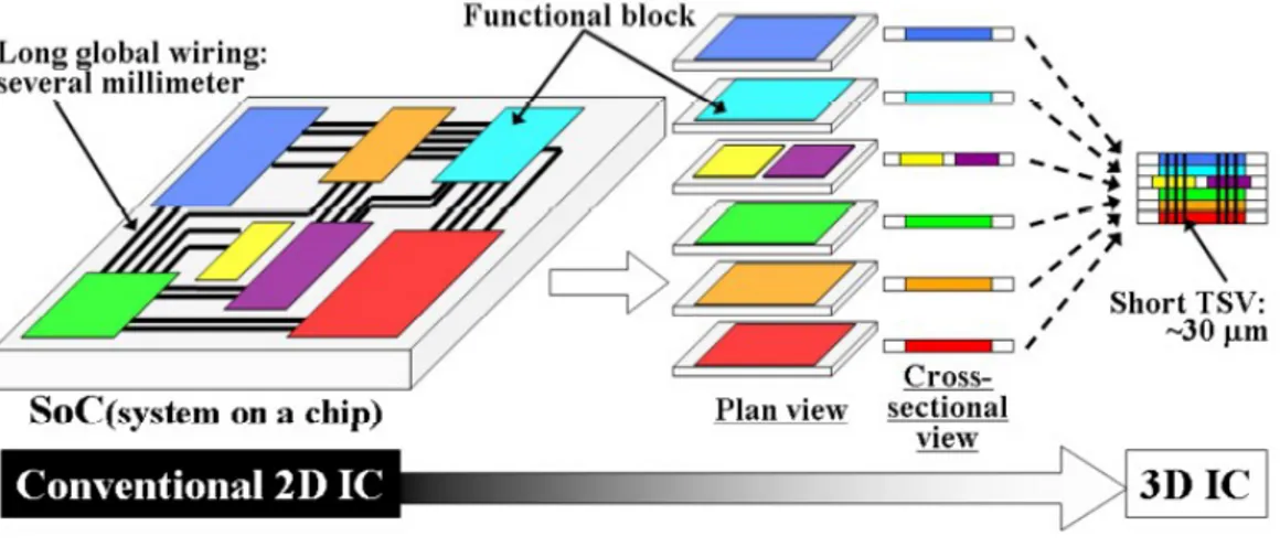
To achieve a higher level of integration ATHENIS3D is proposed to provide the first automotive 3D heterogeneous integration platform using Wafer Level
2 The collection of devices on-board intended to provide entertainment and information: this includes CD/DVD players, TV, Internet connection and
3 It depends on how the vehicle is designed
Packaging (WLP), Through Silicon Vias (TSV) and Integrated Passive Devices (IPD).
The complete system including the battery, the DC-DC converter and the loads to be supplied is shown in figure 4.
The system has to be implemented to match the following specifications.
SYSTEM SPECIFICATIONS:
• Input battery4 voltage V
BAT: 10V(min), 48V(nom), 60V(max); • Average output power POUT: 1,5W;
4 Must meet the new battery standard LV148; see Appendix A for more informations
Figure 3: 3D integration concept using TSV technology.
Figure 4: A schematic block diagram of the entire system: input battery, DC-DC converter and the list of loads to supply.
FPGA Altera Cyclone II: 1,8V 3,3V Hall sensors: 5V H-bridge driver: 12V Other systems: 0,8V DC-DC Converter 48V Battery VBAT VOUT[n]
• Fully integration using WLP, TSV; • -40°C / +150°C;
• Multiple regulated output voltages; • Both step-up/down conversion.
C
HAPTER2 O
VERVIEW OFDC-DC C
ONVERTERSA
RCHITECTURESA DC to DC converter is an electronic circuit which converts the input voltage to a stable output voltage; this justify their use in every portable device such mobile phones, laptops computers and generally in every electric system which are supplied with power from batteries primarily. In general a regulation is required to maintain the desired output voltage independently from line and load variations5.
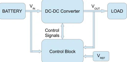
A general block diagram of a regulated DC-DC converter is shown in figure 5.
Independently from the topology implemented the principle of operation is typically the same: the output voltage (and sometimes the input one) is compared to a reference voltage and the resulting error signal is then used to control the DC-DC converter operation; the performance of the complete converter obviously depends on the chosen converter's topology and control technique.
A brief introduction to common control techniques and DC-DC converters
5 Actually due to non-ideal components limit the DC-DC conversion to a specific input voltages and output capability ranges.
Figure 5: General block diagram of a regulated DC-DC converter
DC-DC Converter Control Block V REF LOAD BATTERY Control Signals V IN VOUT
topologies follows: this will be helpful to justify the proposed converter.
2.1 Control techniques for DC-DC converters
As described in the next paragraphs the most commonly used converters uses one or more switches to perform DC-DC conversion. The switches commutes periodically between the ON and OFF states: the effect is that the average output voltage is a function of ON and OFF durations (tON and tOFF). Many algorithms can be used to implement this regulation: here we focus on Voltage Mode Control (VMC), Current Mode Control (CMC), Pulse Frequency Modulation (PFM) and skip regulation schemes.
2.1.1 Voltage Mode Control – VMC
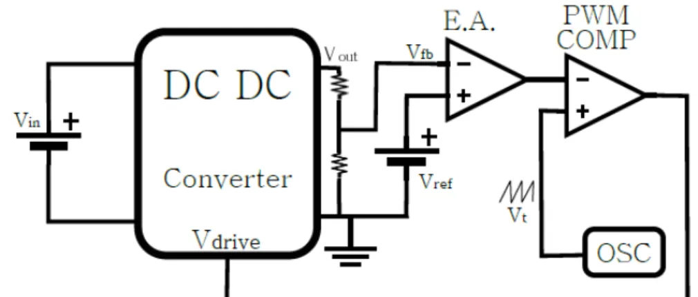
This is the simplest way to control a DC-DC converter. Basically the technique used to control tON and tOFF is the Pulse Width Modulation – PWM. In figure 6 is shown a block diagram of the controller:
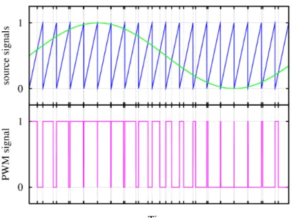
In VMC the divided output voltage and the reference voltage are applied to an error amplifier (E.A.); the resulting error voltage is compared to the saw-tooth signal Vt and the resulting PWM signal is used to turn on and off the switches.
In figure 7 an example of the comparator signals are shown.
Even if this technique is very simple and cheap to implement, there are some drawbacks: a slow output response is not able to compensate input battery voltage and load current fluctuations. Furthermore not sensing the current into the switch it does not prevent its brake if such an error occur.
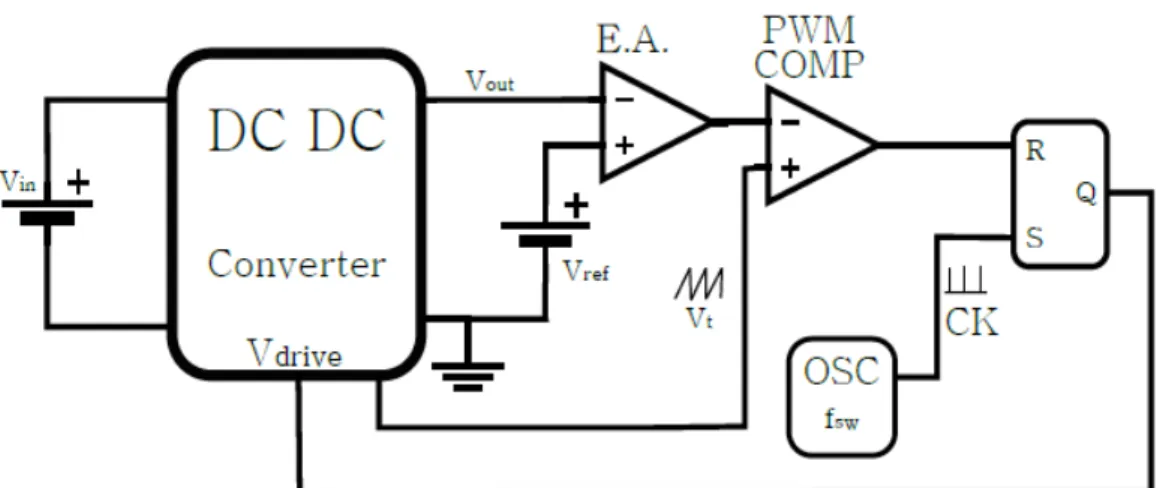
2.1.2 Current Mode Control – CMC
This is an improved version of the VCM control which is commonly used with inductive converters; even if it is a more complicated solution than VCM it leads to a more reliable control. The block diagram is shown in figure 8.
Figure 7: Typical comparator's signals for the VMC regulator: error signal (green), saw-tooth signal (blue) and
In CMC the saw-tooth signal Vt is not necessarily produced by a dedicated generator since it is generated from the current through the inductive element or through the switches. The resulting current-mode control achieves faster response than voltage mode control. Furthermore parallel converter, main switch and overload protection can be easily implemented. However drawbacks still remains: instabilities may occur at duty cycle greater than 50% with sub-harmonic oscillations. Controller's complexity also has to be taken into account.
2.1.3 Other control techniques
Here the functional specifications of two control techniques are described. Their performances are discussed in the following chapters.
Pulse Frequency Modulation – PFM
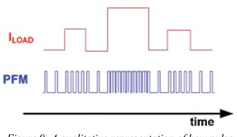
In pulse frequency modulation the controller generates pulses at fixed duty cycle (typically 50%) at a frequency which depends on the input signals. Applying this scheme to DC DC conversion it means that if line or load variations occurs then the controller acts by varying the frequency of the switch control signal. This is qualitatively shown in figure 9.
Skip regulation
Skip regulation is the simplest way to regulate the output voltage in capacitive DC-DC converters. Basically it consists in the comparison between the output voltage and the reference voltage; if the output voltage is greater or equal to the reference voltage the controller skips switching cycle; when the output voltage drops below the reference voltage the oscillator is reactivated and the output voltage increases.
2.2 DC-DC Converters topologies
Two categories of dc dc converters exists: linear and switching regulators. Linear voltage regulators are the simplest converters but they have some drawbacks: the power efficiency is low and the output voltage can't be higher than the input one. Switching regulators (also known as Switching Mode Power Supplies – SMPS) periodically stores energy from the input and release it to the output at a different voltage. Inductors and transformers are used to store magnetic energy and capacitors to store electric energy. Typically power FET's are used as switching elements. These regulators performs the most efficient conversion method; some common drawbacks of switching regulators includes complexity, electronic noise (in terms of
Figure 9: A qualitative representation of how pulse frequency modulation (PFM) works: as the load becomes stronger the switch control signal commutes
EMI/EMC) and cost.
An overview of linear and switching regulator's topologies are described: their principle of operations, the advantages and drawbacks are pointed out.
2.3 Linear Voltage Regulators
This voltage regulator's concept is very simple: the idea is to regulate the load current in order to maintain constant the output voltage. A control loop sense the output voltage and the difference with a reference voltage is used to control that current. A standard architecture is shown in figure###.
In the standard regulator the pass device is a NPN Darlington driven by a PNP to achieve high current gain. Since the pass device has to work like a current generator it must be guaranteed, over the entire operational range, an input-output drop of about 2VBE+VCE; since this value can be likely greater than 1V if the application requires a high current the power efficiency6 dramatically decreases due to the power dissipated on the pass device. To overcome this problem the pass device is typically replaced by a PNP transistor as shown in figure###.
6 The power efficiency of a DC-DC converter is defined as the POUT over PIN= POUT+PLOSS
ratio. It can be demonstrated that linear voltage regulator's efficiency is proportional to the VOUT over VIN ratio.
Now the minimum drop7 is about V
CE which can be few hundreds of millivolts. This kind of linear regulators are also referred to as low drop-out regulators (LDOs). LDOs are still used in a wide range of applications due to their simple implementation.
2.4 Inductive DC-DC Converters
Here are described few inductor-based converters in their operations and the voltage conversion ratio is derived for each topology.
2.4.1 Step down (Buck) converter
An idealized schematic is shown in figure ###. This converter produces an average output voltage which is smaller than the input one. The converter charge the inductor during the first phase (tON) and discharge the stored energy to the output during the second phase (tOFF).
In particular when the switch is closed (tON) the inductor's voltage is Vi-Vo and the current charge it; with the switch open, since the magnetic flux must vary continuously, the current continue to flows through the diode discharging the
stored energy to the output pin.
Assuming an ideal switch, a constant input voltage Vi , an ideal diode and a pure resistive load we can write for inductor current in steady state
∫
0 TS vLdt=0∫
0 tON (vi−vo)dt+∫
tON tON+tOFF (−vo)dt=0 tON(vi−vo)−tOFFvo=0 tONvi=(tON+tOFF)vo vo= tON (tON+tOFF) vi vo=tON TS vi→vo=δviwhere TS=tON+tOFF is the switching period.
It can be seen that the average output voltage is proportional to the duty cycle δ of the control signal.
In the above operation the current in the inductor never reaches zero and it is said that the converter operates in continuous conduction mode (CCM). Otherwise if the current reaches zero during the discharge phase the
converter operates in discontinuous conduction mode (DCM); in this case the average output voltage is given by 8
where Δ is related to the time the current is still not zero.
2.4.2 Step up (Boost) converter
The step up converter is able to produce an average output voltage greater than the input voltage. A common schematic with ideal components is shown in figure ###.
Similarly to what previously done, in the same conditions, we can write for CCM
8 From this general equation it can be obtained the required duty cycle to maintain a constant input voltage or output voltage.
∫
0 TS vLdt=0∫
0 tON vidt+∫
tON tON+tOFF (vi−vo)dt=0 tONvi+tOFF(vi−vo)=0 (tON+tOFF)vi=tOFFvo vo= 1 (1−tON TS ) vi→vo= 1 (1−δ)vi vo vi = δ (δ+Δ)this converter apparently can produce an unlimited output voltage if δ tends
to 1; actually the presence of parasitics elements limits the ratio vo
vi
.
For the DCM the step up converter response is given by
2.4.3 Step-up/Step-down (Buck-Boost) converter
To overcome the limitations of the previous converters a step-up/step-down converter is needed; an ideal scheme is shown in figure ###.
The response of the converter is described in CCM by
and it can be thought as the cascade of the step up and step down converters. Furthermore this converter produces a negative output voltage. In DCM the response becomes
vo=−vi(1−δ)δ
vo=−viΔδ vo
vi
2.4.4 Flyback converter
The Flyback converter is widely used in industry: it is essentially a buck-boost converter where the inductor is replaced by a transformer and the output voltage has the same polarity of the input voltage. An ideal schematic of the converter is shown in figure ###.
For the CCM the output voltage is given by
where n2
n1
is the transformer turns ratio.
Instead in DCM we have
manca formula
2.5 Capacitive DC-DC converters
We have seen that inductive converters uses at least a coil, an output capacitor and two circuit's states: during phase 1 the inductor is in series to the input battery and the coil is charged9 with a current
ICOIL= VI
LCOIL
Δt
9 This phase is also referred to as “pre-charge phase”.
vo=vin2
n1 δ (1−δ)
and during phase 2 the energy stored is transferred10 to the output capacitor. Similarly, capacitive converters uses capacitors instead of coils to store energy during the pre-charge phase.
Therefore switched capacitors DC-DC converters operates in the same way of an inductive converter with the difference that the DC-DC conversion is achieved by using only switches and capacitors. In fact, capacitive converters consists of two distinct types of capacitors: the flying capacitors and a buffer capacitor. The flying capacitors are used to transfer the charge from the input to the output. The buffer capacitor does not transfer charge from the input but it is needed to maintain the output voltage constant;in addition it affect the start-up behaviour of the converter and the steady-state noise characteristics. Today's step-up SC DC-DC converters (also known as charge pumps) are widely used in flash memories to generate the high voltage needed for erasing and writing operations. Their use as voltage regulators is in fact limited to few applications.
Some commercial solutions are listed11 in the table###. Product
Name
Input range Output range Max output current Switching frequency Flying capacitors LM3352 2.5; 5.5V 1.8; 4V 200mA 1MHz 3x 330nF LT1054L 3.5; 7V 5V 125mA 25kHz 10μF LT1515 2; 10V 3/ 3.3/ 5V 50mA 650kHz 220nF FAN5602 -3; 6V 2.7-5.5V 100mA 1MHz 2x1μF
As we can see commercial products does not match our specifications. In the table### a comparison between linear and switching regulators is done.
Linear Voltage Regulators Switching regulators
Inductive Capacitive (inductor-less) Conversion Step-down only Both step-up/down possible
10 This phase is also referred to as “transfer phase”.
type
Complexity Low Mediumto high Simple concept Efficiency High to low12 High Medium to high
Area Very small Mediumto High Small
Cost Low Medium
to High Low
Since our application requires a high level of integration LDOs and capacitive DC-DC converters can be chosen. Furthermore since actually only good quality capacitors are integrable with TSV technology an inductor-less DC-DC converter must be designed and verified.
In general a capacitive converter periodically changes its structure between two or more states13. Here capacitive converters which uses only one flying capacitor and two states are studied.
2.6 Proposed system architecture
Since inductor-less converters must be used, to obtain regulated multiple output voltages it is necessarily to use more instances of the same building blocks. Therefore we have decided to partition the entire system as shown in figure###.
12 It depends on the output to input voltages ratio.
13 Literature offers a wide range of capacitive converter's structures that uses two or more flying capacitors and/or circuit's states but the today's most common solutions uses one flying capacitor and two states.
SC DC-DC
SC DC-DC
LDO LDO LDO
DIGITAL INTERFACE
Immagine
Provvisoria
Where the input battery voltage is regulated by two SC converters to obtain a first 12V output voltage and a second 5V output voltage: this last conversion is also …
C
HAPTER3 P
ROPOSED SWITCHED CAPACITORSDC-DC
CONVERTER MODELLING
Since the first SC DC-DC converter is the most challenging the proposed SC converter is modelled and designed to properly regulate the input battery voltage to 12V output voltage. The implementation of the other blocks are discussed later.
Two methods are used in this work to analyse this kind of circuit: • charge conservation principle
• differential equations
the charge conservation principle approach leads to a simple relation between input and output voltages that can be used to system level specifications. Since this method is typically used on ideal schematics the results does not take into account the effects of parasitics elements. Furthermore since the resulting equation is obtained in a steady-state condition it does not give any information about output ripple and settling time.
The description with differential equations is obtained with the procedure below:
1. graphic representation of the circuit in each phase
2. use of the Kirchhoff Laws (current and voltage) to write a set of electrical equilibrium equations
4. definition of the schematic in terms of Simulink block set
Differently from the previous approach this method is in fact not simply to solve by hand14. On the other hand it is useful to describe a more realistic schematic: the resulting model is therefore simulated for a better understanding of the converter's operations.
The proposed converter is shown in figure### and it is implemented using only one flying capacitor CFLY, a buffer capacitor COUT and four switches.
This architecture offer the possibility to perform both step-up and step-down conversions as will be demonstrated. A control block chooses the conversion type to be used by sensing the input voltage and regulates the converter operations to guarantee a constant output voltage.
3.1 Step-down SC converter
For step-down conversion the switches have to be driven in the following way:
S1 = PH1 S2 = PH2 S3 = CLOSED S4 = OPEN
14 Because the initial conditions changes with the switching activity
+
-V
IN+
-V
OUT+
-V
FLYC
FLYC
OUTS
1S
2S
4S
3 GND GNDIn figure### the corresponding step-down SC converter is shown.
To apply the charge conservation law it is supposed that the on resistance of the switches is zero and ideal capacitors. Imposing the steady-state condition the total charge is conserved during the switching cycle. This means
∑
i
QC ,i(1)=Qout(2)+
∑
iQC ,i(2)
that the total charge at the end of the phase 1 is equal to the total charge at the end of the phase 2 plus the charge drawn by the load during the entire switching period.
In particular, during phase 1, the CFLY is charged up to the input voltage VI and COUT is at VOUT. When the circuit is in phase 2 CFLY is connected in parallel to COUT so they share the same voltage VOUT. The total charge drawn by the current load is IL/fSW. In other words, and finally,
+
-V
IN+
-V
OUT+
-V
FLYC
FLYC
OUTS
1S
2 GNDCFLYVI+COUTVOUT=CFLYVOUT+COUTVOUT+ILOAD
VOUT=VI− ILOAD
fSWCFLY
This equation shows that the maximum possible voltage conversion ratio for this topology is 1 as expected from a step-down converter. Furthermore the output voltage decreases linearly with the load's current at a given switching frequency fSW and flying capacitor CFLY.
3.1.1 Step-down SC converter model
To define the step-down converter model two parasitic resistors are added to the converter schematic as shown in figure###: RP1 and RP2 represents the on resistances of he switches; finally the capacitor's ESR can be included in the RP1 and RP2 computation.
Applying KCL and KVL to the step-down topology during each phase we obtain: 26 GND
+
-V
IN+
-V
OUT+
-V
FLYC
FLYC
OUTS
1S
2I
LOADR
P1R
P2+
-V
IN+
-V
OUT+
-V
FLYC
FLYC
OUTS
1S
2I
LOADR
P1R
P2 GND VI=RP1Cf dVf dt +Vf dVo dt = −ILOAD COCFLYVI=CFLYVOUT+ILOAD
for the phase 1 and
for the phase 2.
And if we reorder them to point out the derivative of the voltages we have:
during the phase 1 and
during the phase 2.
Integrating these equations and solving for the variables Vf and VO we have the solution for the step-down converter. To simplify the process Simulink is used for this operation and the block diagrams in figure### are obtained. These equations leads to the model shown in figure###.
0=CFdVf dt + Vf RP2 − VO RP2 −ILOAD=CO dVO dt + VO RP2 − V f RP2 dVf dt = VI −Vf RP1CO dVO dt = −ILOAD CO dV f dt = 1 RP2CO (VO −Vf) dVO dt = −ILOAD CO +Vf −VO RP2CO
3.2 Step-up SC converter
To perform the step-up conversion the switches have to be driven as follows: S1 = S3 = PH1
S2 = S4 = PH2
Therefore in this mode all the switches commutates. The corresponding architecture is recalled in figure###.
As previously done the charge conservation is applied on a period. We can write: and finally,
+
-V
IN+
-V
OUT+
-V
FLYC
FLYC
OUTS
1S
2S
4S
3 GND GNDCFLYVI=CFLY(VOUT −VI)+ILOAD
fSW
CFLYVI+COUTVOUT=COUTVOUT+CFLY(VOUT −VI)+ILOAD
fSW
VOUT=2 VI − ILOAD
the input-output relationship is obtained. We can see that the output voltage continue to decrease linearly with output current with the difference that the maximum output voltage can be twice the input one.
3.2.1 Step-up SC converter model
The step-up converter is modelled in the same way than before. In figure### it is shown the step-up converter during each phase.
Applying KCL and KVL we obtain:
+
-V
IN+
-V
OUT+
-V
FLYC
FLYC
OUTS
1S
2S
4S
3 GND+
I
LOAD+
-V
IN+
-V
OUT+
-V
FLYC
FLYC
OUTS
1S
2S
4S
3 GND+
I
LOAD VI=RP1Cf dVf dt +Vf dVo dt = −ILOAD COfor the phase 1 and
for the phase 2.
Finally, reordering the equations, we have:
and
for phase 1 and 2 respectively.
These equations are therefore used to build the model shown in figure###. −ILOAD=COdVO dt +Cf dV f dt VO −VI=RP2Cf dVf dt +V f dVO dt = − ILOAD CO −CF CO dVf dt dVf dt = VO −VI −Vf Rp2Cf dVf dt = VI −Vf RP1CO dVO dt = −ILOAD CO
3.3 Control block modelling
In this work three control methods are considered and modelled; • Pulse Width Modulation – PWM
• Pulse Frequency Modulation – PFM • SKIP Control
Finally, the topology control block is briefly described.
PWM CONTROL
This is a well-known control method as it is used in a wide range of applications. Since its widely usage we have decided to investigate its utilization in SC DC-DC converters control.
The block diagram of the PWM controller is shown in figure###.
The difference between output and reference voltages is used to compute
the relative error ϵr=VREF −VO
VREF
which is limited15 by the saturation block;
the error signal is therefore compared to the sawtooth signal to produce the switch control.
PFM CONTROL
PFM control continuously modulates the frequency of the pulses signal controlling the switch. For the sake of simplicity we have decided to modulate the frequency linearly respect to the error voltage.
Therefore,
fSW(t)= f0+KVVerror(t)
where fSW(t) is the instantaneous frequency of the switch control signal, f0 is the free running frequency16, V
err(t) is the voltage error and KV is the proportional coefficient. To implement this relationship we have decided to use it as argument of a cosine function and the output is compared to zero to obtain the squared switch control signal.
Therefore we consider the general sinusoidal oscillation
where θ is the instantaneous phase. Since the instantaneous frequency fSW(t) is defined as
16 Defined as the switching frequency at zero error voltage.
we can write that
and finally,
cos (θ(t))=cos (2 π f0 ⋅t+2 π KV
∫
Verr(t)dt)this equation leads to the block diagram shown in figure###.
fSW(t)= 1 2 π d θ dt θ=2 π
∫
fSW(t)dt θ=2 π∫
f0+KVVerr(t )dt θ=2 π f0 ⋅t+2 π KV∫
Verr(t)dtSKIP CONTROL
Skip control simply skips switching cycles when a condition occurs: in particular when the output voltage is greater than the reference voltage the comparator disables the oscillator; when the output voltage decreases and becomes smaller than the reference voltage the comparator enables the oscillator and consequently the switch control signal makes the output voltage to increase. During this operation switch control signal
This functionality is modelled with the block in figure###. Later it is demonstrated that skip control is the best control method: to better understand the impact of a non ideal comparator on the control loop we have included the comparator's offset voltage and the comparator's delay.
The use of a D flip-flop is necessarily to guarantee a 50% duty cycle to the switch control signal.
Topology control block
We have shown that different switches configuration decides up or step-down conversion. This is implemented by comparing the input battery voltage to a reference voltage: the comparator's output is used as logical variable to decide the switches configuration.
3.4 Complete step-up/down SC converter model
To work with a unique model of the regulated SC converter all the previously blocks are used to build such a model which is shown in figure###.
Finally, a top level representation has been build in order to make the parameters selection simple. This is shown in figure###.
All the converter's parameters are therefore accessible through the configuration mask in figure###.
3.5 Parameters selection
Looking at the equationsVOUT=VI − ILOAD
fSWCFLY VOUT=2 VI − ILOAD
describing the steady-state response of the open loop step-up/down SC converters we observe that for a given output capability, an input voltage range and a desired output voltage the remaining quantities represents the design parameters.
Such a parameters are the switching frequency fSW and the flying capacitor CFLY. In addition the output capacitor COUT has to be chosen accordingly to match the other requirements17. Finally, R
P1 and RP2 parasitic resistors are critical in switch selection.
To choose the switching frequency and the flying capacitor we consider the following specifications:
• 12V desired output voltage
• 10V minimum input battery voltage • 120mA output capability
Inverting the ideal open loop step-up18 characteristic
we obtain,
This “equivalent resistor” takes into account the drop between the input and output voltages when a given current is drawn19. Non ideal devices are expected to increase this equivalent resistance. For this reason we have
17 As previously explained the output capacitor does not participate to charge transfer but its value affect the transient response, the output ripple and the maximum impulsive charge that the load can absorb.
18 Since the input battery voltage is smaller than the desired output voltage.
19 In other words, the equivalent resistor consider the charge that it is transferred over a switching period for an ideal circuit: this means that all the charge is transferred from the input to the output pins. Therefore it is expected that if a fraction of this charge flows into different nodes, the amount of charge which is transferred to the output capacitor is smaller. Consequently the output voltage is smaller than expected.
VOUT=2 VI − ILOAD fSWCFLY 1 fSWCFLY= 2×10 −12 0.12 ≈67Ω
decided to consider an equivalent resistor smaller of about 25%.
Therefore, 1
f SWCFLY=50 Ω is the value considered.
To select the switching frequency and the flying capacitor the approach used is intended to obtain the smaller switching frequency20.
The frequencies chosen and the corresponding flying capacitors are shown in the table###.
fSW [KHz] CFLY [nF]
200 100
500 40
Since the integration of passive devices is a constraint and the maximum integrable capacitor size is about 40nF21, 500KHz is the chosen switching frequency.
The output capacitor selection is made considering that it must maintain as constant as possible the output voltage. This means that during the pre-charging phase the output capacitor have to drop lesser than a specific ΔVOUT. Using the capacitor's constitutive equation
and imposing a total drop ΔVOUT during the period Δt with an average current ILOAD we obtain the minimum output capacitor values shown in table###.
ΔVOUT [mV] 22COUT [μF] 23QPEAK [μC]
20 Otherwise if the integration of the flying capacitor is a requirement the switching frequency has to be sufficiently high; the technology used in this work allows to integrate up to 1nF but it is costly in terms of area (about 10mm2). Even if area occupation is not a
concern the corresponding high frequency of 20MHz is not manageable. Therefore this solution is not considered.
21 This is the actual TSV capability: about 5nF/mm2 and a maximum value of 40nF.
22 This value is computed considering Δt=1/2*fSW=1μs and ILOAD=120mA; the nearest commercial
and most available value is listed
23 Computed using Q= C*ΔV and considering an acceptable drop of 250mV
ILOAD=COUTΔVOUT
50 2,2 0,55
25 4,7 1,17
10 10 2,5
In addition, given an output capacitor value, the corresponding peak charge QPEAK is listed.
To choose which control block is the most effective we consider the parasitic resistors negligible24.
3.6 Model simulation and preliminary results
In order to test the performance of the converter a parametric simulation has been performed. In particular the simulations results are obtained varying the following quantities:
VI
ILOAD
Control method
with a desired output voltage of 12V.
The performance of the converter is strictly related to its capability to produce a constant output voltage and to maintain it independently from line or load variations. Three metrics are used to measure these capabilities:
output voltage ripple
the load25 and
24 In other words their presence has not to modify the charge and discharge of the flying capacitor: in our case values smaller than 1Ohm are usable.
25 Load regulation is defined as the measure of the circuit's ability to maintain the specified output voltage under varying load conditions. Load regulation is defined as
ΔVOUT
ΔIOUT
the line26 regulation
To cover the DC-DC converter's operating conditions as input battery voltage we consider the worst, the nominal and the best conditions:
For each of those input battery voltage the load's current varies among nominal, high and light conditions27:
Therefore the resulting test-bench used to evaluate the regulated SC converter is shown in figure###.
test-bench The results of the simulation activity28 at f
SW=500kHz is shown in table###. Control
type COUT [μF] time [μs]Settling Max outputripple regulationLine regulationLoad PWM 2,2 38 800mV 4mV/V 1,25V/A PFM 7mV/V 1,25V/A SKIP 7mV/V 0,83V/A PWM 4,7 80 400mV 4mV/V 0,25V/A PFM 4mV/V 0,92V/A SKIP 3,4mV/V 0,20V/A PWM 10 165 200mV 3mV/V 0,13V/A PFM 1,8mV/V 0,48V/A
maximum rated value or vice versa at nominal input battery voltage.
26 Line regulation is defined as the measure of the circuit's ability to maintain the specified output voltage with varying input voltage. Line regulation is defined as
ΔVOUT
ΔVI
at the nominal output current. Input voltage transitions from its minimum to its maximum rated values.
27 The nominal condition corresponds to an output power of about 1,5W at 12V. The light condition's current is due to the presence of a resistive output voltage divider. And the high load and light load conditions have been chosen arbitrarily as the double and the 1/10 of the nominal current.
28 More simulations have been performed: the results can be found in Appendix###.
{120mA , 240mA ,12mA } {10V , 48V , 60V}
SKIP 1,2mV/V 21mV/A
From the simulation's results of the ideal29 converter it can be seen that the choice of the control type is not critical since the performance metrics are of the same order of magnitude. This is because the flying capacitor is always charged to the input battery voltage and completely discharged on the output capacitor. Due to this fact the charge regulation is not effective.
If parasitic resistors are considered30 equal to 8,333Ω in the model simulation the corresponding results are shown in table###.
Control
type COUT [μF] time [μs]Settling Max outputripple regulationLine regulationLoad PWM 2,2 60 100mV 32mV/V 3,07V/A PFM 40 600mV 6mV/V 1,31V/A SKIP 600mV 6mV/V 1,09V/A PWM 4,7 170 60mV 33mV/V 3,07V/A PFM 100 400mV 3mV/V 0,438V/A SKIP 90 400mV 2,8mV/V 0,657V/A PWM 10 350 10mV 40mV/V 3,3V/A PFM 190 200mV 1,06mV/V 0,26V/A SKIP 190 200mV 1,2mV/V 0,26V/A
It is now necessarily to make some considerations about these results: • An increase in the output capacitance leads to an increase of the
settling time and a decrease of the output voltage ripple. Approximately as the output capacitance double, so as the settling time; while the output voltage ripple is halved.
• Given a certain output capacitance, the output voltage ripple is better in PWM rather than in PFM or SKIP, unlike line and load regulations.
29 The (RP1,2 CFLY) time constant is smaller than 1/2fSW.
Due to the fact that PFM and SKIP gives almost the same results and since SKIP control is more simple, to save area, we have decided to implement SKIP control.
In addition, since there is no specification on settling time or output voltage ripple we have chosen the smallest output capacitance to decrease the simulation time31.
To design the regulated converter it is helpful to look at the voltages at each node: here we consider the step-up/down converter with skip regulation32.
PER IL DCDC COMPLETO SCELTO LE FORME D'ONDA AD OGNI NODO... QUESTO CI FARA' COMODO NELLA FASE DI DESIGN....
COME INFLUISCONO LE RESISTENZE PARASSITE SULLE PRESTAZIONI...
SI VEDE CHE LE PRESTAZIONI MIGLIORANO TRANNE SETTLING TIME CON L'AUMENTARE DELLA COUT....SE VOGLIO BUONE PRESTAZIONI E SETTLING TIME BUONO POSSO USARE UNA COUT PICCOLA E REGOLATORE PI
AGGIUNGERE ALLE TECNICHE DI CONTROLLO UN CENNO AL REGOLATORE PID ED ALLE SUE CARATTERISTICHE PIU IMMEDIATE. MAGARI IN APPENDICE METTO TUTTE LE SIMULAZIONI SIMULINK ED ANCHE L'AGGIUNTA DEL PI
31 For the design activity.
C
HAPTER4 D
ESIGN OF A STEP-
UP/
DOWNSC DC-DC
CONVERTERIn this chapter the design of the regulated SC DC-DC converter is described and the main issues are pointed out.
4.1 The HV 350nm CMOS technology
The technology used in this work is the ams HV 350nm CMOS: this paragraph intends to illustrate some peculiarities of the MOSFETs that can be realized.
The equivalent models are shown in figure###. Figure equivalent models
These MOSFETs have the following maximum absolute ratings: VDS,MAX= 120V
VGS,MAX= 5.5V VBSUB,MAX= 120V
In addition these MOSFETs are designed to have the drain to the highest potential respect to the source: this fact has important consequences in the design.
4.2 The switches
When a MOSFET is used to implement a switch two quantities must be considered: the on resistance33 R
DS(ON) and the gate charge QGATE that is
33 We recall that the on resistance defined in the linear operating condition where the drain's current is given by IDS=KPW
L [(VGS−VTn)VDS+ V2DS
2 ] ; if we consider a good
overdrive and a VDS≈0 we have the following approximation for the on resistance:
RDS (ON )=vDS
iDS
≈ L
necessary to turn on and off the gate.
Also if both N and P MOS can be used as switch there are some important trade off to consider in MOS type choice; in fact, choosing NMOS, rather than PMOS, results in a smaller switch since the electron's mobility is up to 3 times greater than the hole's mobility. Unfortunately to switch on a NMOS we need a gate voltage greater than the maximum drain's voltage plus a threshold voltage or VG>max VD+VTn ; This is a problem since we need of a charge pump to drive the gate. This results in an increase of design effort. On the other hand if PMOS is used, the corresponding area is greater (about 2 to 3 times) than NMOS with the same on resistance but the complexity is highly reduced. The PMOS in fact has to be driven to ensure at least a threshold voltage under the drain's voltage. We have,
VG<VD+∣VTp∣
Now, to choose the MOSFET type, we have to consider the voltages at each node during a complete switching cycle. In addition, since actual switching cannot be instantaneous, we consider the presence of intermediates states: during these states the switches are not closed nor opened.
Let us consider the step-down topology first in figure###. figure step-down waveforms per tensioni
As we can see from the figure the drops across the switches S1,S2, S3 and S4 have always the same polarity. This means that there is no concern about the PMOS during step-down conversion.
It is different if the step-up converter is analysed (figure###). Figure step-up waveforms per tensioni
In fact, it is evident that the voltage drop across S1 and S2 varies its polarity during the step-up conversion. This is a problem since to switch on a PMOS a positive VSD is needed. This problem does not involve the switches S3 and
S4.
4.2.1 Symmetric MOSFETs
To solve the voltage drop's polarity across the switches S1 and S2 it is necessary to use the so called symmetric34 MOSFET.
The MOSFET in figure### is the symmetric one obtained from two separate HV PMOS described before.
Figure the symmetrical MOSFET
Furthermore, the bulk B has to be driven to the highest instantaneous potential to keep always reversed biased the parasitic diodes.
Since it is required some time to change the Bulk potential it is expected that for a given interval the parasitic drain diode is in conduction: since the bulk potential is anyway greater than the substrate potential, the corresponding pnp bipolar transistor is forward biased. Therefore the current flows into the substrate causing an increase in the substrate potential and a leakage of current. These phenomena can become critical for safety35 and efficiency36 and must be carefully analysed.
4.2.2 Main switch sizing
In SKIP control the on resistance of the switches has to be small enough to allow a full charge and discharge of the flying capacitor. This value has already been estimated previously: imposing that the on resistance is such
that 3 RONCFLY≤ 1
2fSW we obtain RON(TOTAL) ≤ 8,333Ω; In addition, since there are three MOSFETs in series during each phase, dividing by three, we obtain the on resistance of a single MOSFET: RON(SINGLE MOS) ≤ 2,777Ω;
34 It can manage both positive and negative VSD.
35 The forward biased pnp transistor can switch on the parasitic SCR; this is the latch-up. 36 The leakage current corresponds to a charge quantity that does not flows to the output
Now, to size the single MOSFET, the on resistance per μm37 must be evaluated.
Therefore, the NMOS an PMOS are simulated in the worst corner38 to guarantee the specified on resistance.
From the simulation we have obtained the following results: NMOS: RDS(ON)= 21405 Ω*μm
PMOS: RDS(ON)= 132800 Ω*μm
Dividing these values by the desired on resistance we obtain the size of the MOSFET:
NMOS: L=1μm; W≈7700μm PMOS: L=1μm; W≈47821μm
An approximation for the gate charge QG is given by the CGATE*VGATE product; if we consider39 C
GATE ≈ CGS and VGATE=VSG=5V we have the following table. CGS QG
PMOS 120pF 600pC NMOS 20pF 100pC
4.2.3 Bulk switch sizing
We have already introduced, for the symmetrical MOSFET, the necessity to drive the bulk to the highest potential. Here the sizing of these switches is described.
To change the bulk potential it is necessarily to change the charge in it. The
37 With a fixed length of L=1μm.
38 TJUNCTION=150°C and worst speed corner which means the highest threshold voltages.
bulk switches commutes and the required charge flows through the turn on switch. Since the on resistance of the bulk's switches is initially high the voltage drop is consequently high: if the voltage drop is too high it can forward bias the parasitic diode of the main switch causing the safety and efficiency concerns previously described. Therefore it is necessarily that the on resistance is sufficiently small to avoid these problems.
We have chosen the size of the bulk switches as follows:
SizeBulkSwitch = SizeMainSwitch /10
The validity of this rule of thumb has been proved in this way: starting from a small MOSFET, the charge injected in the main switch's bulk and the on resistance have been measured. Increasing the MOSFET's size we have observed a decreasing for the on resistance and for the charge injected. Finally, despite the on resistance's decrease, an increase of the charge injected and of the current which flows through the bulk switch have been observed and any increase of the bulk switch's size results in a greater capacitance drain-bulk. The results are listed in the table###.
Size ratio40 1/240 1/20 1/10 1/5
QBULK 460pC 206pC 26pC 52pC
RON 380Ω 47Ω 22Ω 12Ω
Finally, for bulk switches we have L=1μm; W≈4782μm.
4.3 Gate driver
We have estimated the charge that is needed to completely turn on the MOSFETs: the gate charge. The circuit which provide that charge is called
gate driver.
In this work we have decided to turn on and off the switches in 10ns. Therefore the capability of the gate driver has to be at least
IGateDriver=CGS ΔV
Δt = QGATE
Δt =60mA ; Furthermore, to completely turn on the
PMOS, the gate voltage must be 5V smaller than the source voltage. Figure### MOSFET con gate driver
The gate driver that has been used is a level shifter: its simplified schematic is shown in figure###
figure### level shifter used
4.4 Bulk driver
Also the bulk switches must be driven: for this particular task it is necessary to use an as fast as possible gate driver able to drive the bulk potential to the highest voltage. Therefore, it must be able to compare two voltages and quickly decides which is at the highest voltage.
The circuit used is shown in figure### in a simplified form. Figure### bulk driver basics
4.5 Control block
The control block performs two tasks:
• sensing the output voltage, it controls the commutation of the switches in order to maintain an as constant as possible output voltage,
• and, sensing the input battery voltage, it controls the conversion type that must be used.
4.5.1 SKIP control
The4.5.2 Topology control
4.6 Simulation
CHAPTER 5 CONCLUSIONS AND FUTURE DEVELOPMENTS
RIGUARDO AL SYSTEM ARCHITECTURE BISOGNA CONSIDERARE CHE SE RIUSO LA CELLA SC DCDC CONVERTER SICCOME L'INGRESSO E' ORA REGOLATO NON HO PIU BISOGNO DEI PMOS120M E QUINDI RIDUCO A BESTIA L'AREA E IL LIMITE EVENTUALMENTE MI E' DATO DALLE CAPACITA'. COMVIENE QUINDI LDO O SC-DCDC?
R
EFERENCES [1] [2] [3] [4] [5]A
PPENDIXA: LV148
NEW48V
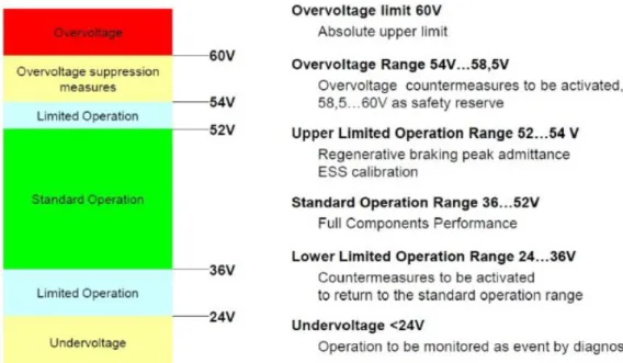
BATTERY STANDARDlevels are shown in figure A1.
APPENDIX B: COMMERCIAL SOLUTIONS TO SC DC-DC
CONVERSIONHere are shown some examples of data sheets of commercial SC converters: