UNIVERSITA’ DEGLI STUDI DI
CATANIA
DIPARTIMENTO DI INGEGNERIA ELETTRICA,
ELETTRONICA ED INFORMATICA
Concetta Signorello
REDUCTION OF SWITCHING LOSSES
IN IGBT POWER MODULES
Tesi di Dottorato di Ricerca Internazionale in Energetica
XXVII Ciclo
Coordinatore:
Chiar.mo Prof. Ing. Luigi Marletta
Tutor:
Chiar.mo Prof. Ing. Mario Cacciato
~ 2 ~
INDICE
INTRODUCTION ... 4
FIRST PART - THEORETICAL ASPECTS CHAPTER 1 - IGBT ... 7
1.1. Controllable Switches ... 7
1.2. Architectural and Physical characteristics ... 9
1.2.1. Basic structure ... 11
1.2.2. IGBT characteristics ... 14
1.2.3. Comparison with Power MOSFET ... 16
1.3. Operating mode ... 17
1.3.1. Block mode operation (OFF state) ... 18
1.3.2. Conduction mode operation (ON state) ... 19
1.4. Operating faults: the Latch-up... 20
1.5. Switching characteristics ... 23
1.5.1. Turn ON ... 26
1.5.2. Turn OFF ... 29
1.5.3. High temperature characteristics ... 32
1.5.4. Real or Ideal behavior of the IGBT ... 33
1.6. Operation Losses ... 33
1.6.1. Operation losses of an IGBT ... 36
1.6.2. Reduction of Overcurrent at Turn-ON ... 38
1.6.3. Reduction of Overvoltage at Turn-OFF ... 39
1.6.4. Conduction losses and Switching losses ... 39
1.7. Problems related to dv/dt ... 40
1.8. Safe Operating Area (SOA) ... 40
1.9. Application Area of IGBT ... 42
CHAPTER 2 - THE DRIVER ... 45
2.1. IGBT driver design considerations ... 47
2.2. Structural features ... 48
~ 3 ~
2.2.2. Isolation between primary and secondary sides ... 49
2.2.3. Secondary side of driver circuit ... 49
2.2.4. Isolation of the triggering signal using an optocoupler ... 50
SECOND PART - EXPERIMENTAL ASPECTS CHAPTER 3 - DRIVING TECHNIQUES ... 52
3.1. Driving open loop - Hardswitching ... 52
3.2. Driving closed loop - Feedback Techniques ... 55
3.2.1. Independent control of dv/dt and di/dt through feedback on the gate voltage ... 55
3.2.2. Dynamic control of dv/dt with active clamping ... 65
3.2.3. Active control of the collector voltage by feedback with preconditioning Bias voltage ... 68
CHAPTER 4 - A NOVEL TECHNIQUE ... 71
4.1. Independent control of dv/dt and di/dt through feedback on the gate voltage using a monostable circuit ... 71
4.1.1. Operating principle ... 71
4.2. Comparison between the driving techniques ... 79
CONCLUSIONS ... 83
~ 4 ~
INTRODUCTION
Power modules are electronic components that are formed by semiconductor devices. These power devices have appeared on the market for the first time in 1975 and immediately have obtained a large success in the world of Power electronics.
Their applicability must be considered under the following aspects: “optimized“ complexity of a module, heat dissipation capability, isolation voltage and partial discharge stability, static and dynamic symmetry of the structure, electromagnetic stability, defined and safe failure behavior, simple assembly and connection technology, low-polluting production and recyclability.
The purpose of this work is to study in deep the transition phenomena of IGBTs in order to evaluate different optimization strategies for losses reduction and propose a novel technique.
The IGBT devices are increasingly used in electronic circuits both for their ease of driving that for their ability to handle high currents and voltages at high switching frequencies.
Increasing devices switching speed is possible to reduce the power dissipation with the disadvantage of an increase of electromagnetic interference (EMI) and overcurrents. In fact, with increasing di/dt during switching transients EMI are increased, so it is necessary to specify the design of any power converter, the right tradeoff between switching speed, energy losses, EMI, overvoltages and overcurrents.
In electronic systems for power conversion, the driver circuit is the interface between the control circuit and power devices. The main function of the driver consists in amplifying the control signals, in order to supply the energy requested by the power devices to change their state from interdiction to saturation and vice-versa.
~ 5 ~
In power applications a particular attention must be taken to such phenomena as commutation losses, overcurrents during the turn-ON and overvoltage at the turn-OFF of the devices.
These phenomena are connected to non ideal behavior of real devices and stray circuit parameters. Steep profiles of current lead to large ElectroMagnetic Interference (EMI) and overvoltages, while rapid variations of the voltage can produce phenomena of "latch-up" in single IGBT or unwanted commutations. On the other hand, slow commutations are characterized by low values of dv/dt and di/dt, causing excessive losses in those power application during commutations.
One of the main goals in design the driver stages of power converters is the reduction of the commutation losses, obtaining remarkable benefits in terms of reduction of the dissipation and, consequently, the chance to increase the switching frequency. In order to reduce the commutation losses, the simplest way consists in shorting the time of commutation by rising the gate current lowering gate resistance value. These benefits are paid with the increasing complexity of the driving circuits, the greater difficulties in their design and higher final costs.
Therefore, it is essential to face the issue with opposite requirements at the design stage obtaining optimal tradeoff.
~ 6 ~
~ 7 ~
CHAPTER 1 - IGBT
The insulated-gate bipolar transistor (IGBT) is a three-terminal power semiconductor device primarily used as an electronic switch and in newer devices is noted for combining high efficiency and fast switching. It is used in many modern applications: variable—frequency drives (VFDs), electric cars, trains, variable speed refrigerators, air-conditioners and even stereo systems with switching amplifiers. Since it is designed to turn ON and OFF rapidly, amplifiers that use it often synthesize complex waveforms with pulse width modulation and low-pass filters.
1.1. Controllable Switches
IGBTs are controlled switches, in which the "ON and OFF states" are fixed by a control signal. Ideally when the switch is open no current flows and when it is closed the current can flows in only one direction.
The most commonly used devices as switches in today's industrial applications are power BJT, MOSFET and IGBT.
The BJT and MOSFET Transistors are complementary in many aspects regarding their behavior.
In BJT the effect of base conductivity modulation means that the voltage drop between drain and source is small and independent of the collector current. This is due to the high number of minority carriers in the depletion region when the device operates in saturation, unless achieved particularly high injection levels. This means that the BJT have low conduction losses.
In MOSFET Transistors, larger values of output resistance ON-State and the absence of a conductivity modulation effect give rise the voltage drops between drain and source much more than BJTs. Consequently the conduction losses will be greater.
~ 8 ~
If in the BJT the output resistance and voltage drop, in saturation region, are independent of the size of the device that has tied the value of breakdown voltage, in the MOSFET these values depend on the technological characteristics of the device, such as doping and thickness of different layers. So the BJT although characterized by low values of resistance in conduction and high voltage blocking capabilities, have numerous limitations among which include the low switching speed and high current driving. The MOSFET overcome these problems in that they are driven in voltage with high switching speed, at the expense of conduction losses.
Then the MOSFET Transistors are better than BJTs.
The advantages of MOSFET Transistors are switching speed and the possibility of driving voltage devices. The benefit is a reduction in overall switching losses during power transients. The voltage control allows simple drivers because you can avoid to provide high current device. IGBTs take the best part of these two types of transistor, the high input impedance and high switching speeds of a MOSFET with the low saturation voltage of a BJT and combines them together to produce another type of switching power device that is capable of handling large collector-emitter currents with virtually zero gate current drive.
The IGBT is a fairly recent invention. The first-generation devices of the 1980s and early 1990s were prone to failure through such modes as latchup (in which the device will not turn OFF as long as current is flowing) and secondary breakdown (in which a localized hotspot in the device goes into thermal runaway and burns the device out at high currents). Second-generation devices were much improved, and the current third-generation ones are even better, with speed rivaling MOSFETs, and excellent ruggedness and tolerance of overloads.
The IGBT combines the simple gate-drive characteristics of MOSFETs with the high-current and low-saturation-voltage capability of bipolar transistors. It combines an isolated gate FET for the control input, and a
~ 9 ~
bipolar power transistor as a switch, in a single device. The IGBT is used in medium mode power supplies, traction motor control and induction heating. Large IGBT modules typically consist of many devices in parallel and can have very high current handling capabilities in the order of hundreds of amperes with blocking voltages of 6000 V, equating to hundreds of kilowatts.
IGBT, for its structural and functional characteristics, is presented as a compromise solution between MOSFET and BJT combining the major qualities of both.
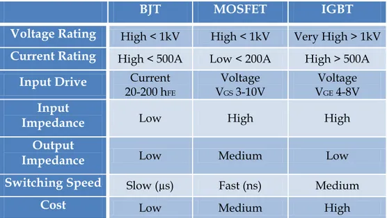
In the table 1 are shown the main advantages and disadvantages of the controlled devices.
ADVANTAGES DISADVANTAGES
BJT Low conduction losses Current driving
Slow switching
MOSFET Voltage driving
Fast switching High conduction losses
IGBT
Voltage driving Fast switching
Low conduction losses High breakdown voltage
Latchup Current tail
Tab. 1 - Advantages and Disadvantages of controlled devices.
1.2. Architectural and Physical characteristics
The Insulated Gate Bipolar Transistor (IGBT) uses the insulated gate, hence the first part of its name, technology of the MOSFET with the output performance characteristics of a conventional bipolar transistor, hence the second part of its name. The result of this hybrid combination is that the “IGBT Transistor” has the output switching and conduction characteristics of a bipolar transistor but is voltage-controlled like a MOSFET.
IGBTs are mainly used in power electronics applications, such as inverters, converters and power supplies, were the demands of the solid state switching device are not fully met by power bipolars and power
~ 10 ~
MOSFETs. High-current and high-voltage bipolars are available, but their switching speeds are slow, while power MOSFETs may have high switching speeds, but high-voltage and high-current devices are expensive and hard to achieve.
The advantage gained by the insulated gate bipolar transistor device over a BJT or MOSFET is that it offers greater power gain than the bipolar type together with the higher voltage operation and lower input losses of the MOSFET. In effect it is an FET integrated with a bipolar transistor in a form of Darlington configuration as shown in Figure 1.
Fig. 1 - Circuit symbol of IGBT device.
It is possible to see that the insulated gate bipolar transistor is a three terminal, transconductance device that combines an insulated gate n-channel MOSFET input with a PNP bipolar transistor output connected in a type of Darlington configuration. As a result the terminals are labeled as: Collector, Emitter and Gate. Two of its terminals (C-E) are associated with a conductance path and the third terminal (G) associated with its control.
The Insulated Gate Bipolar Transistor can be used in small signal amplifier circuits in much the same way as the BJT or MOSFET type transistors. But as the IGBT combines the low conduction loss of a BJT with the high switching speed of a power MOSFET an optimal solid state switch exists which is ideal for use in power electronics applications.
~ 11 ~
When used as static controlled switch, the insulated gate bipolar transistor has voltage and current ratings similar to that of the bipolar transistor. However, the presence of an isolated gate in an IGBT makes it a lot simpler to drive than the BJT as much less drive power is needed.
An insulated gate bipolar transistor is simply turned “ON” or “OFF” by activating and deactivating its Gate terminal. A constant positive voltage input signal across the Gate and the Emitter will keep the device in its “ON” state, while removal of the input signal will cause it to turn “OFF” in much the same way as a bipolar transistor or MOSFET.
1.2.1. Basic structure
The IGBT is a semiconductor device with four alternating layers (P-N-P-N) that are controlled by a metal - oxide - semiconductor (MOS) gate structure without regenerative action.
Semiconductors are solids characterized by a band structure with a full valence band and a empty conduction band separated by a gap with an energy of the order of one or a few electron volts. At room temperature only a few electrons have sufficient energy to enter the empty band, so as to be able to conduct.
An important characteristic of semiconductors is also to have, in addition to electrons, a second type of charge carriers, able to generate a current: excited electrons into the conduction band leave the free states in the valence band, which allow for some mobility to other electrons left. This motion is described as the motion of a positive hole.
The main reason for which the semiconductors are so useful is that the conductivity of semiconductors can be modified with the addition of impurities (doping), with the action of an electric field, with exposure to light, or by other means.
~ 12 ~
With reference to the vertical section of a generic n-channel IGBT shown in the Figure 2(a) you can see the analogy with the typical structure of a vertical MOSFET in Figure 2(b). [3]
Fig. 2 - (a) Vertical section of an n-channel IGBT; (b) Vertical section of an n-channel MOSFET.
The main difference is the addition of a p+ type layer which is the collector of the device. This layer forms with that above a pn junction and it is responsible for injecting minority carriers in n+ and n- layers which are in fact the drain region of a MOS structure with vertical development. The wide n- region, known as the drift region or LDB (Low Doped Base), along with the body (p) and substrate (p+) form a pn-p+ which can be considered as a pnp BJT.
The drift region (n-) allows to the IGBT to withstand high voltages because lightly doped, while the n+ region has the dual function of controlling the gain of the transistor and to limit the emptying of the gate-collector
(a)
~ 13 ~
junction avoiding this reaches the emitter. Similar considerations apply for
p-channel IGBT.
It is important to note that due to its intrinsic constitution, the structure of IGBTs contains a thyristor parasite whose activation is potentially destructive to the device. A constructive precaution aimed at reducing the probability of accidental ignition of the parasitic thyristor is to extend the emitter metallization above the body region.
The presence or absence of the layer n+ inside the structure of the device, classifies the IGBTs in two different types: [21]
NPT IGBTs (Non Punch Through) without layer n+; PT IGBTs (Punch Through) with layer n+.
NPT PT
Switching Loss
MEDIUM Long tail current Moderate increase in EOFF with temperature
LOW Short tail current Significant increase in EOFF with temperature
Conduction Loss Increases with MEDIUM
temperature
LOW
Flat to slight decrease with temperature
Tab. 2 - Characteristics Comparison of NPT and PT IGBTs.
So the IGBT can be seen how the connection of a Power MOS and a BJT
pnp type whose base is connected to the drain of the PMOS. Therefore the
IGBT presents the Power MOS characteristics in the input and the BJT characteristics in the output.
A general comparison between BJT's, MOSFET's and IGBT's is given in the following table 3.
~ 14 ~
BJT MOSFET IGBT
Voltage Rating High < 1kV High < 1kV Very High > 1kV
Current Rating High < 500A Low < 200A High > 500A
Input Drive Current
20-200 hFE Voltage VGS 3-10V Voltage VGE 4-8V Input
Impedance Low High High
Output
Impedance Low Medium Low
Switching Speed Slow (µs) Fast (ns) Medium
Cost Low Medium High
Tab. 3 - Comparison between IGBT, MOSFET and BJT devices.
We have seen that the Insulated Gate Bipolar Transistor is semiconductor switching device that has the output characteristics of a bipolar junction transistor, BJT, but is controlled like a metal oxide field effect transistor, MOSFET.
One of the main advantages of the IGBT transistor is the simplicity by which it can be driven ON or OFF or in its linear active region as a power amplifier. With its lower ON-state conduction losses and its ability to switch high voltages without damage makes this transistor ideal for driving inductive loads such as coil windings, electromagnets and DC motors.
1.2.2. IGBT characteristics
As shown in Figure 3, the current-voltage characteristics of an n-channel IGBT device appear similar to those of a BJT (the region of direct polarization), except for the control parameter that is the voltage between gate and emitter (VGE) instead of the gate current.
~ 15 ~
Fig. 3 - Current- Voltage characteristics of IGBT devices.
The curve is linear in the range of allowed values of the VGE above the threshold voltage VGE(th). After the curve is not linear. The VGE(th) represents the value of voltage applied between the collector and emitter that separates the ON state (VGE >VGE(th)) from the OFF state (VGE<VGE(th)). Because the IGBT is a voltage-controlled device, it only requires a small current on the Gate to maintain conduction through the device unlike BJT’s which require that the gate current is continuously supplied in a sufficient enough quantity to maintain saturation.
Also the IGBT is a unidirectional device, meaning it can only carries the current in the “forward direction”, that is from Collector to Emitter unlike MOSFET’s which have bi-directional current switching capabilities (controlled in the forward direction and uncontrolled in the reverse direction).
The principal of operation and Gate drive circuits for the Insulated Gate Bipolar Transistor are very similar to that of the n-channel power MOSFET. The basic difference is that the resistance offered by the main conducting channel when current flows through the device in its “ON” state is very much smaller in the IGBT. Because of this, the current ratings are much higher when compared with an equivalent power MOSFET.
The main advantages of using the Insulated Gate Bipolar Transistor over other types of transistor devices are its high voltage capability, low ON-resistance, ease of drive, relatively fast switching speeds and combined with zero gate drive current makes it a good choice for moderate speed, high voltage applications such as in pulse-width modulated (PWM),
~ 16 ~
variable speed control, switch-mode power supplies or solar powered DC-AC inverter and frequency converter applications operating in the hundreds of kilohertz range.
1.2.3. Comparison with Power MOSFET
An IGBT features a significantly lower forward voltage drop compared to a conventional MOSFET in higher breaking down voltage rated devices. As the blocking voltage rating of both MOSFET and IGBT devices increases, the depth of the n- drift region must increase and the doping must decrease, resulting in roughly square relationship decrease in forward conduction versus breaking down voltage capability of the device. By injecting minority carriers (holes) from the collector p+ region into the
n- drift region during forward conduction, the resistance of the n- drift region is considerably reduced. However, this resultant reduction in ON-state forward voltage comes with several penalties:
The additional pn junction blocks reverse current flow. This means that unlike a MOSFET, IGBTs cannot conduct in the reverse direction. In bridge circuits, where reverse current flow is needed, an additional diode (freewheeling diode) is placed in parallel with the IGBT to conduct current in the opposite direction. The penalty isn't overly severe because at higher voltages, where IGBT usage dominates, discrete diodes are of significantly higher performance than the body diode of a MOSFET.
The reverse bias rating of the n- drift region to collector p+ diode is usually only of tens of volts, so if the circuit application applies a reverse voltage to the IGBT, an additional series diode must be used.
The minority carriers injected into the n- drift region take time to enter and exit or recombine at turn ON and turn OFF. This results
~ 17 ~
in longer switching times, and hence higher switching loss compared to a power MOSFET.
The ON-state forward voltage drop in IGBTs behaves very differently from power MOSFETs. The MOSFET voltage drop can be modeled as a resistance, with the voltage drop proportional to current. By contrast, the IGBT has a diode-like voltage drop (typically of the order of 2V) increasing only with the log of the current. Additionally, MOSFET resistance is typically lower for smaller blocking voltages, so the choice between IGBTs and power MOSFETs will depend on both the blocking voltage and current involved in a particular application.
In general, high voltage, high current and low switching frequencies favor IGBTs while low voltage, low current and high switching frequencies are the domain of the MOSFET.
1.3. Operating mode
From an operational point of view, the IGBT can be regarded as constituted by an n-channel MOS in input and by a pnp BJT in output. The two devices are connected in Darlington configuration (Fig. 1), act as a primary device (BJT) and driver (MOS) respectively.
The MOS section determines the state of IGBT's operation, while the BJT section determines the blocking voltage between Collector and Emitter or the transport of charge between them, according to the mode in which the device is to operate (OFF/ON ).
~ 18 ~
1.3.1. Block mode operation (OFF state)
In the OFF state, the behavior of an IGBT is equal to that of a MOSFET. The voltage applied between the Gate and Emitter determines the status of the device. For values of VGE<VGE(th) there isn't formation of the inversion layer in the section of the MOSFET in input. In these conditions, the IGBT is turned OFF, the voltage between Collector and Emitter of the
pnp bipolar transistor of the output section is supported by the p+n -junction, in Figure 2(a) is J2 junction. The doping level of the p+ and n -regions is fixed so as to extend the depletion region of the junction J2 inside the drift region.
You can see that the maximum voltage applied between Collector and Emitter of the IGBT depends on the thickness of the drift region, which must contain the depletion region J2. If the layer of n+ type was absent, so for a NPT IGBT, the capacity to block reverse depends on the depth of the drift region, and can be made equal to that direct.
The ability to direct sealing of the device depends on the characteristics of the drift region: greater is its thickness, the higher is the value of the voltage that the device can support in the output. Unfortunately, the same parameter is also linked to the resistance value of the collector-emitter path in the ON state, increasing with it. In NPT devices an increased ability to block direct the device produces an increase in the output resistance in the ON state and therefore an increase of conduction losses. In PT devices you exceed this problem by introducing a thin n+ layer in the p+ region of the collector when the value of the output voltage exceeds the limit value of the thickness of the n- layer. In this way, in the PT devices is possible to realize a drift region thinner than that of a NPT IGBT, maintaining the same output voltage.
The advantage is in the reduction of conduction losses, the disadvantage is a reduced of blocking reverse ability.
~ 19 ~
1.3.2. Conduction mode operation (ON state)
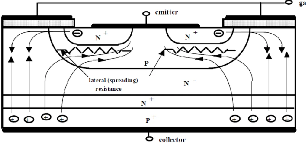
In the ON state, there are the working mechanisms of the MOS and BJT. In Figure 4 is described the operation of the ON state of an IGBT. [3, 10]
Fig. 4 - Conduction mode operation of the IGBT.
When the VGE>VGE(th) you can see the formation of an inversion layer charge in the body region under the Gate contact. For high values of VGE the n-channel puts into short-circuits the drift region (n-) and the Emitter region (n+). The result is an electron current flowing from one region to another through the n-channel, like a MOSFET. But the IGBT has another layer of p+ type. This layer produces an injection of positive charges that can make up for the electron flow generated in the upper layers. The holes move through the drift region is to diffusion that derives in various directions. So you can see how the structure formed by the body, the drift region and the drain behaves as a bipolar transistor pnp type.
It is thus justified the Darlington configuration used to represent the IGBT shown in Figure 1, while in Figure 5 are shown, with the respective symbols, the MOS and BJT sections present in the device.
~ 20 ~
Fig. 5 - MOS and BJT section into IGBT.
In the IGBT, the voltage drop which has in conduction state is smaller than that of a PowerMOS of equal characteristics.
To understand the reason, should be considered the intrinsic voltage drops that occur between the Collector and Emitter. Applying Kirchoff's law is obtained by the following relationship:
The Vp+n is a typical bias voltage of the pn junction and its value is approximately in the range 0.7 - 1.0 V. The Vdrift is much smaller than that of the Power MOS due to an effect of conductivity modulation of the drift region due to the injection of minority carriers from the p+ region, as happens in the BJT. The Vch depends on the ohmic resistance of the channel and it is the same like a MOSFET. The effect is to reduce the voltage drop at the output of the IGBT device compared to Power MOS.
1.4. Operating faults: the Latch-up
The IGBT contains a parasitic pnpn thyristor structure between the Collector and the Emitter.
A latch-up means the turning ON of the thyristor. When there is action by a thyristor, the IGBT current is no longer controlled by the MOS gate. The IGBT would be destroyed because of excessive power dissipation
~ 21 ~
produced by the amount of current over the rated value between the Collector and the Emitter.
During ON-state, paths for current flow in an IGBT are shown in Figure 4. The holes are injected into the n- drift region from the p+ collector form two paths. Part of the holes disappear by recombination with electrons came from MOSFET channel. Other part of holes are attracted to the vicinity of the inversion layer by the negative charge of electrons, travel laterally through the p-body layer and develops a voltage drop in the ohmic resistance of the body. This voltage tends to forward bias the n+p junction and if it is large enough, substantial injection of electrons from the emitter into the body region will occur and the parasitic NPN transistor will be turned-ON. If this happens, both NPN and PNP parasitic transistors will be turned-ON and hence the thyristor composed of these two transistors will latch on and the latchup condition of IGBT will have occurred. Once in latchup, the gate has no control on the collector current and the only way to turn-OFF the IGBT is by forced commutation of the current, exactly the same as for a conventional thyristor.
If latchup is not terminated quickly, the IGBT will be destroyed by the excessive power dissipation. IGBT has a maximum allowable peak drain current (ICM) that can flow without latchup. Device manufacturers specify this current level in the datasheet. If this current level is exceeded in static conditions, with the device in the permanent ON state, a large enough lateral voltage drop will activate thyristor and the latchup of IGBT.
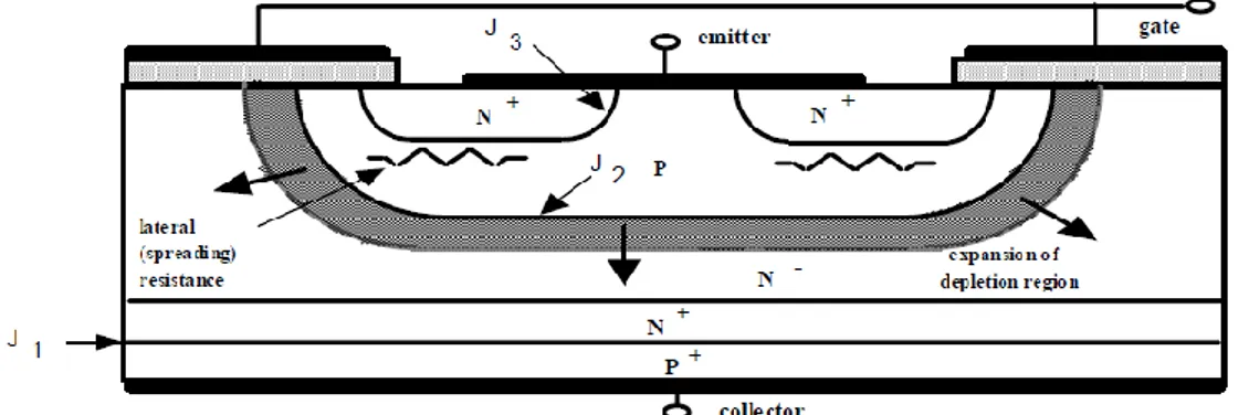
In Figure 6 is shown a circuit model of the IGBT which concerns the phenomenon of latchup and the parasitic thyristor which generates it. In dynamic conditions (Figure 7), during switching, the value of the collector current in which occurs the latchup is lower than that recorded in static conditions. During turn OFF, in fact, the rapid switching OFF of the MOS part of the device and resetting of the current through this part produce a sudden increase of the voltage on the collector supported by the
~ 22 ~
pn-junction formed by the drift region and body region, inversely
polarized. [3, 21]
Fig. 6 - Equivalent circuit with parasitic thyristor.
Fig. 7 - Expansion of the depletion region in the drift region, which can cause latchup dynamic.
There are two approaches to reduce the probability of initiation of the parasitic thyristor and the consequent destruction of the device latchup. The first one, the technology, is to adopt a series of constructive measures designed to reduce the value of the leakage resistance of the body which is associated with the potential drop which triggers the phenomenon.
The second one, that user, involves the design of mechanisms that on the one hand prevent the occurrence of static and dynamic overcurrent, on the other hand slow turn OFF of the device so as to reduce the expansion speed of the depletion region in the drift region so that the holes can recombine before you get to body. But excessive slowing of the switching of the device results in an excessive increase of the switching losses.
~ 23 ~
An increase in the gate resistance due to a slowing down of switching, from the ON state to the OFF state or vice versa. Since the dynamic latchup only affects the process of switching off, it is useful to decouple the resistive check on the gate by introducing two different resistors, one for power ON and one for power OFF. This allows it to act directly on the speed of the IGBT switching OFF without interfering with the switching ON.
These solutions may be insufficient to find a good compromise between the many conflicting requirements related to the switching of the devices and of which latchup and switching losses represent only one part.
The aim of this work is to find the right tradeoff by designing a good driving circuit for IGBT.
1.5. Switching characteristics
The switching characteristics of an IGBT are very much similar to that of a Power MOSFET. The major difference from MOSFET is that it has a tailing collector current due to the stored charge in the n- drift region. The current tail increases the turn OFF loss and requires an increase in the dead time between the conduction periods of two devices in a half-bridge circuit. Consider the vertical section of an n-channel IGBT shown in Figure 8.
~ 24 ~
Fig. 8 - Parasitic capacitances in the IGBT.
There are many parasitic capacitive phenomena that influence the switching transients. They may, however, be traced back to three fundamental capabilities: Cce, Cge and Cgc.
The first one concerns all parasitic capacitive effects between Collector and Emitter of the device, the second one relates the parasitic capacitive effects between Gate and Emitter of the device and the third one concerns the parasitic capacitive effects between Gate and Collector of the device.
The Cce can be ignored because it doesn't affect the switching characteristics. Instead, the capacity Cge and Cgc aren't constant during turn ON and turn OFF, but changes with the voltage applied to them. The most significant changes affecting the Cgc as the voltage jump which it is subject during a switching is far higher than the Cge. So the variations of Cgc are the only ones which are taken into account in the analysis of transient. They are continuous and non-linear as is shown in Figure 9.
~ 25 ~
Fig. 9 - Variation of Cgc depending on the voltage between collector and emitter.
For simplicity, in order to calculate the waveforms of switching, it was considered appropriate to identify the Cgc with two discrete values: Cgc1 and Cgc2, one of starting and the other of arrival. The transition from one value to another occurs the instant that the vce and the vge are equal. This is the moment of entry or exit of the device from the ohmic region.
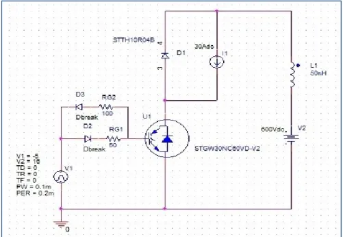
In Figure 10 is shown the circuit commonly used to study the switching behavior of a generic power IGBT and reproduces the working conditions of a device inserted in a DC-DC converter or an inverter. This circuit allows us to measure the electrical quantities during the switching transient, as well as the energy losses.
~ 26 ~
The current generator I1 ideally represents an inductive load as, for example, an electric motor. It can be assumed, approximately, that the current through the load during a switching cycle is constant. This current is imposed on the circuit due to the highly inductive nature of the load and the energy stored in it. Hence the use of the ideal current generator to model the inductive load.
The recirculation diode D1 is connected in antiparallel to the load in order not to pass current when the load is powered.
The gate resistors RG1 and RG2 work by controlling parameter on the speed of transition between ON and OFF states and their value strongly influences the output gradient of the voltage and the current (dv/dt and
di/dt) in the process of switching.
The ideal voltage generator V1 provides pulses of appropriate amplitude acts to force the switching. It represents the real driving circuit of the device (driver).
The generator V2, however, provides blocking voltage of the device during turn OFF transition.
The device U1 is the IGBT under test.
1.5.1. Turn ON
The following figure shows the waveforms of the voltage and current that characterize the transition from the OFF to the ON states of the IGBT operating in an inverter. [1, 11, 16, 17, 18]
~ 27 ~
Fig. 11 - Turn ON characteristics of an ideal IGBT.
Assuming at first VGE = 0 and assuming that at time t = 0 the generator V1 (VGG) imposes a positive voltage step of amplitude greater than the threshold voltage VGE(th) will see the evolution of the electrical quantities of the input and output shown in the Figure 11.
During the delay time td(on) the voltage VGE(t) increases from zero to VGE(th) due to the currents that flow in the capacity Cge and Cgc.
The pattern in which the VGE(t) grows can be considered approximately linear, although it is to be understood as the initial part of an exponential with a slope given by the time constant
In this first phase the VGE(t) changes, while collector voltage and current do not change. When the gate voltage reaches the threshold begins a second phase of the turn ON indicated by the time lag tri. The instant in which the
~ 28 ~
gate voltage equals the threshold value, the collector current starts to grow.
In the ideal case, the effects of overcurrents related to secondary phenomena are ignored (reverse recovery current of a not ideal diode), for which the collector voltage is constant until the current is not equal to its static value in the ON mode (Ion). In the real case, however, these effects are evident and consequently also the collector voltage has the same problems. The following figure shows interference of the real case.
Fig. 12 - Turn ON characteristics of an real IGBT. The blue waveform represents the gate voltage,
the violet waveform the collector current and the green waveform represents the collector voltage.
Just finishing the transient current, start a third phase of switching in which the gate voltage stands at a constant value. This value is necessary to sustain the collector current Ion.
The time interval during which the gate voltage is constant is called
Region of Miller. This assumes a very important role in the development of
optimization techniques for the control of IGBT devices. The duration of this interval is equal to tfv1 + tfv2.
As mentioned previously, the gate voltage is constant in Miller region. In tfv1 happens a rapid decrease of the output voltage. In tfv2 the VCE(t)
~ 29 ~
continues to decrease but with different slope. In fact, at this stage, it is assumed that the device is entered in the ohmic region, and, as mentioned previously, the final value of the Cgc is equal to Cgc2. The decrease in the slope of the VCE(t) must be attributed to the increase of Cgc.
The Cgc changes continuously and not linear between the minimum and the maximum value identified by Cgc1 and Cgc2. This phenomenon is called Miller Effect. Outside the Region of Miller the voltage between gate and emitter to grow back to move to the value imposed by the generator input.
The time constant with which the VGE evolves exponentially towards its final value is
While the voltage between Collector and Emitter is equal to VCE(on).
In power applications, where the devices are used in switching mode, at the end of turn ON is always VGE >> VGE(th).
From all this it is clear that the voltage and current gradients are dependent on the gate resistance RG. A reduction of RG involves an increase of the speed of switching and vice versa.
The RG as the only control parameter represents a limit. In fact, an increase in the dv/dt by a reduction of the RG, at turn OFF, contributes to the reduction of the switching losses. But the reduction of RG increases the
di/dt that can generate overvoltages and electromagnetic interference (EMI)
unwanted. Similar words apply to the turn ON. So a need to develop techniques capable of influencing separately control the profiles of voltage and current. The aim of this work is to explore these possibilities.
1.5.2. Turn OFF
For the study of the switching OFF of an IGBT is possible to follow a similar approach to turn ON. In this phase, the device presents a
~ 30 ~
phenomenon known as current tail which determines a significant slowdown with a consequent increase of the switching losses. [1, 11, 16, 18] The test circuit used is the same (Figure 10).
The following figures show the waveforms of the voltage and current that characterize the transition from the ON to the OFF states of the IGBT operating in an inverter. In Figure 13 the ideal behavior and in Figure 14 the real behavior of an IGBT.
~ 31 ~
Fig. 14 - Turn ON characteristics of an real IGBT. The blue waveform represents the gate voltage,
the violet waveform the collector current and the green waveform represents the collector voltage.
From a qualitative assessment has perfect symmetry between ON and OFF states in relation to the sequence of events and the evolution of the variables, except for the final stretch (interval tfi2). In a totally specular to turn ON, the instant witch the driver force a negative step on the gate, the voltage VGE starts to decrease at an exponential rate and the time constant related to the parasitic capacitances Cgc and Cge.
During the interval td(off), the collector voltage and the current remain unchanged and the only electrical quantity that changes is the VGE. After reaching the threshold VGE(th), the VGE stands at VMiller constant value as in power ON. In the range of Miller (trv) the collector current is constant while the collector voltage VCE changes.
In the ideal case being absent overvoltages tied to parasitic inductances present in the power side of the circuit, the collector voltage reaches its final value in correspondence of the Miller region. At the same time the extinction of the voltage transient begins the current transient. This starts to decrease in two phases: tfi1 and tfi2.
In the interval tfi2 the current has a sharp reduction in slope that causes a slowdown in switching. This phenomenon is caused by the bipolar section
~ 32 ~
of the IGBT. That is, the positive charges trapped in the drift region in the second phase of the power OFF. In fact, the MOS section of the device, very fast, is the first to turn OFF. At the end of tfi1 can be closed switching of the input section of the IGBT.
This happens before the charges present in the drift region have had time to drain away. The timing and effectiveness are related to the life time of the excessive charges. The life time is linked to the value of RCE(on). The higher the life time of the charges and the lower the RCE(on), and the smaller the conduction losses. It is therefore necessary to find a compromise between:
contain the conduction losses through a reduction in RCE(on);
contain the switching losses by reducing the lifetime of excess carriers.
It is also noted that the phenomenon of the current tail is characterized by a positive temperature coefficient. The duration of the phenomenon increases with increasing temperature, which in turn depends on the power dissipated. This increases with the current tail. So it triggers a dangerous process that leads to the destruction of the IGBT. It is appropriate to find a compromise position between two features. The solutions to the problem of the current tail can be found exclusively in technology.
1.5.3. High temperature characteristics
The minority carrier lifetime in the drift region increases as the temperature increases. This not only delays recombination process (current tail) of the minority carrier, but it also increases the PNP transistor gain. So the portion of the initial abrupt fall in the overall collector current reduces. As such, tf (fall time) of the spec is lengthened, and turn-OFF time increases with an increase in temperature.
~ 33 ~
1.5.4. Real or Ideal behavior of the IGBT
Ideally the power devices must be able to tolerate high voltages in the OFF state, conduct high currents with low voltage drops in the ON state and be able to quickly switch between ON and OFF states.
An ideal switch must have the following characteristics:
Blocking direct and reverse voltages of any magnitude without conducting current in the OFF state;
Conducting any current with no voltage drop across its terminals in the ON state;
Switch from ON to OFF and vice versa quickly; Request small quantity of power for driving.
All real devices show a behavior that is very different from the ideal one. In particular, commutations not instantaneous, a voltage drop different from zero in the ON state and small leakage current in the OFF state produce a power dissipation due to joule effect, which in extreme cases can lead to destruction of the device to excessive overheating.
1.6. Operation Losses
An ideal totally controlled device has the following features:
It is able to withstand direct and reverse voltages of any amplitude with zero current in OFF state;
It conducts currents of any amplitude with insignificant voltage drop;
It is able to instantly switch from ON to OFF states and vice versa; It absorbs powers negligible for the trigger.
The real devices haven't these characteristics and, therefore, during operation they have losses that can irreversibly destroy itself. [1, 3, 11, 16, 17, 18]
~ 34 ~
In Figure 15 is shown a complete switching cycle for a generic switch.
Fig. 15 - Switching characteristics and relative loss in a controlled device.
For simplicity, we consider ideal devices so that the waveforms are linearized and neglect secondary phenomena which can be overcurrents during turn ON and overvoltages during turn OFF.
In Figure 15 are shown: (a) the signal input of the switching, (b) the electrical characteristics, (c) the power and the energy losses.
During power up, after a delay time td(on) with respect to the application of the step voltage on the gate, begins the current transient to reach the steady-state value I0. For the duration of the current transient tri, the output voltage is unchanged. Once the current transient has ended the output voltage reaches the steady-state value VCE(on) during the time period tfv. It is evident that for a time equal to tc(on) = tri + tfv the device is having to support a current and a voltage simultaneously different from zero.
Under the hypothesis of linear waveform characteristics, this involves a dissipation of energy that can be quantified by the following relation:
~ 35 ~
The same happens to turn OFF and the dissipated energy is described by the following equation:
During the conduction phase the current is equal to I0. This generates a small voltage drop VCE(on) which depends on the output resistance of the device in the ON state.
The energy dissipated during the conduction mode is given by:
The sum of the three energies gives us the value of the total energy lost during a switching cycle.
Figure 15(c) shows the waveform of the instantaneous power lost during a complete switching cycle, obtained as the product of current and voltage. The average value of the lost power is obtained by multiplying the energy expenditure in a switching cycle for the working frequency of the switch fs. The average power dissipated is approximately given by:
The power lost due to non-ideal switching devices depends linearly on the frequency. So, to reduce switching losses involves a dual advantage. In fact, if the frequency fs remains constant efficiency of the device increases, because it will be subject to less thermal stress. Conversely, for the same maximum power lost, it is possible to increase the working frequency as required by modern control techniques.
In conduction mode, the average power dissipated is given by:
It can be considered negligible the contribution of the leakage current in the OFF state. So, the total average power dissipated by a switch is equal to:
~ 36 ~
From the expressions derived for the switching and conduction losses, can be easily deduce the desirable features for a switch:
low values of the reverse current;
low values of the voltage drop to reduce the conduction losses; switching times tc(on) and tc(off) very small in order to use the device
at high values of fs;
ability to conduct high current values and to support high values of reverse voltage;
low values of power to switch the device;
ability to withstand the rated voltage and current at the same time to avoid the use of external protection circuits ("snubber" circuits); ability to withstand high values of di/dt and dv/dt to avoid the use of
external circuits for their limitation.
1.6.1. Operation losses of an IGBT
Now we can calculate the losses in an IGBT. To make a realistic estimation some not-ideal characteristics should be taken into account. For this reason, the test circuit to which reference should be made now, shown in Figure 16, takes into account the parasitic inductances in the current paths causing overvoltage shutdown. It will not also neglected the reverse recovery current of the freewheeling diode, due to overcurrent at turn ON. [4]
~ 37 ~
Fig. 16 - a) Test circuit with parasitic inductance; b) Output current and voltage during switching.
The energy lost in power ON is given by:
IRM introduces the contribution given by the not ideal recirculation diode. In fact, the IC has an overshoot with respect to the steady-state value due to the reverse recovery current of the diode. This overcurrent is linked to the di/dt. The VCE has a small negative step V before dropping the final saturation value. The V, takes into account the voltage drop across parasitic inductance Lp. So the voltage across the device becomes:
The average power dissipation is obtained by multiplying Wc(on) for fs, thus obtaining:
At turn OFF the energy lost is given by the sum of the contributions for the three time intervals t0, t1 and t2. t0 and t1 characterize the switching OFF of the MOS section of the IGBT, while t2 is related to the effect of the current tail in the drift region. The total energy lost in power down is:
~ 38 ~
The average power dissipation is obtained by multiplying Wc(off) for fs, thus obtaining:
1.6.2. Reduction of Overcurrent at Turn-ON
The gate resistor (RG) controls the IGBT collector current slope. The choice of this resistor is based on a compromise between reduced power consumption (which requires a low value of RG) and a tolerable dv/dt or
di/dt in order to limit the peak current due to the recovery diode and the
electromagnetic interference (EMI) generation requiring a high value of RG. The latching current depends upon the gate resistance value. The manufacturers suggest a minimum gate resistance value to avoid the latching phenomenon. IGBT drivers are generally implemented using two resistors: one resistor is employed at ON and the other one for turn-OFF. Advanced methods are proposed to limit di/dt and dv/dt based on the feedback control of the IGBT collector current or the collector voltage slope. However, it is not easy to achieve these complex methods, which require considerable silicon area.
In order to protect the IGBT from over-current, risk of latch-up and to limit the EMI, without incurring any increase in the values of gate resistance and the power consumption, the gate voltage must be increased in two separate stages. By increasing the gate to an intermediate stage for a short time before the final turn-ON, the IGBT collector current and its slope di/dt are limited. Hence, the peak current due to the diode reverse recovery is reduced.
~ 39 ~
1.6.3. Reduction of Overvoltage at Turn-OFF
If there is a short-circuit or over-current in the load, a large voltage overshoot can occur across the IGBT at turn-OFF and can exceed the IGBT breakdown voltage. It is proposed to drive the IGBT by applying a signal on the gate with two different stages. By reducing the gate voltage to an intermediate level for a short time before the final turn-OFF, the IGBT collector current is limited and hence the potential overshoot is reduced.
1.6.4. Conduction losses and Switching losses
At any given time, the energy dissipated in the IGBT can be obtained with the following expression:
where t is the length of the pulse. Power is obtained by multiplying energy by frequency, if applicable. When the transistor is OFF i(t)=0 and losses are negligible. Unfortunately, no simple expression can be found for the voltage and current functions when the IGBT is conducting. Hence, for analytical expediency, we resort to the distinction between conduction and switching losses.
Defining conduction losses the losses that occur between the end of the turn-ON interval and the beginning of the turn-OFF interval, as defined for the switching losses characterization. Since the turn-ON energy is measured from 5% of the test current to 5% of the test voltage and the turn-OFF energy is measured starting from 5% of the test voltage, conduction losses occur when the voltage across the IGBT is less than 5% of the test or supply voltage. The function VCE(i) in the formula above characterizes the conduction behavior of the IGBT.
Losses in hard switching have been broken down into two components: turn-ON and turn-OFF losses, as described in paragraph 1.5.
~ 40 ~
1.7. Problems related to dv/dt
The operation of an IGBT can meet a series of issues related to high values of dv/dt. You can have two cases.
dv/dt in static conditions
We talk about dv/dt in static conditions when an IGBT that is in OFF state suffers a transient variation of its collector voltage. This change of voltage is reflected in input through the capacity Cgc and Cge, generating a voltage change on the gate able to turn ON the device. Another effect is due to the possible activation of the parasitic thyristor which can destroy the device.
dv/dt in dynamic conditions
The dv/dt belongs to the operation of any switch. During turn OFF of an IGBT can be seen a rapid expansion of the depletion region which causes an unwanted peak current. This creates the conditions for the occurrence of latch-up.
1.8. Safe Operating Area (SOA)
The safe Operating Area (SOA) is defined as the current-voltage boundary within which a power switching device can be operated without destructive failure. For IGBT, the area is defined by the maximum Collector-Emitter voltage VCE and collector current IC within which the IGBT operation must be confined to protect it from damage. The IGBT has the following types of SOA operations: Forward-Biased Safe Operating Area (FBSOA), Reverse-Biased Safe Operating Area (RBSOA) and Short-Circuit Safe Operating Area (SCSOA). [3, 21]
The IGBT has robust SOA both during turn ON and turn OFF. Figure 17 (a) shows the FBSOA. On the left side it is restricted by the forward voltage drop characteristics. Up to maximum continuous collector current this voltage remains reasonably constant at a low value. However, at ICM this
~ 41 ~
voltage starts increasing as the IGBT starts entering active region. On the top the FBSOA is restricted by ICM.
Fig. 17 - Safe operating area of an IGBT. (a) FBSOA; (b) RBSOA.
The other two limits are formed by the maximum power dissipation limit and the maximum forward voltage limit. Like other devices the maximum power dissipation limit increases with reduction in the on pulse width. The RBSOA for low values of dv/dt is rectangular. However, for increased
dv/dt the upper-right hand corner is progressively cut out. The reason for
this restriction on the RBSOA is to avoid dynamic latch-up. The device user can easily control dv/dt by proper choice of Vgg and the gate drive resistance.
A very important requirement imposed on the power switching device, when used in motor control applications is that be able to turn-OFF safely due to a load or equipment short circuit. When a current overload occurs, collector current rises rapidly until it exceeds that which the device can sustain with the applied gate voltage. The key to survivability for the power device is to limit the current amplitude to a safe level for a period of time that is sufficiently long to allow the control circuit to detect the fault and turn the device OFF.
~ 42 ~
1.9. Application Area of IGBT
In a social background where it is indispensable to take action concerning the environment, power devices have the main role of efficiently using resources and energy in power electronics, and are thus growing increasingly more important.
Based on offering power devices designed for "low power loss" and "miniaturization," the companies dealing to produce intelligent power modules, which are at the forefront of the inverter products market.
The main criteria in choosing either IGBT or MOSFET are voltage rating, power losses (efficiency of the whole system) and of course the cost of the whole system. Choosing one over other may impact not only losses in the transistors but also the weight and cost of cooling, size of the complete product and also reliability so sometimes e.g. a weight constrain may force you to use MOSFET instead of IGBT. [1]
Looking at the graph below, you will see different areas, where each type of switch are typically used:
Fig. 18 - Current/Voltage/switching frequency domains of the main power electronics switches.
Choosing a particular device type depends on specific application and its requirements.
~ 43 ~
MOSFETs dominate in high frequency and low current applications because they can switch extremely fast and act as resistance when ON. Fast switching means they are used when the device has to be small as when you increase switching frequency you can reduce the size of passive filters.
The conduction losses are proportional to the square of drain current and therefore you cannot pass huge current through the structure.
So the power MOSFET has the advantages of a majority carrier device, so it can achieve a very high operating frequency, but it cannot be used with high voltages; as it is a physical limit, no improvement is expected in the design of a silicon MOSFET concerning its maximum voltage ratings. However, its excellent performance in low voltage applications make it the device of choice for applications with voltages below 200 V. By placing several devices in parallel, it is possible to increase the current rating of a switch. The MOSFET is particularly suited to this configuration, because its positive thermal coefficient of resistance tends to result in a balance of current between the individual devices.
IGBTs have higher breakdown voltage and conduction losses are approximately equal to Vf*Ic therefore you can use them in high current applications. They have limited switching speed therefore they are typically used in industrial applications where low switching frequency is not a problem (acoustical noise).
The IGBT is a relative recent component, so its performance improves regularly as technology evolves. It has already completely replaced the bipolar transistor in power applications; a power module is available in which several IGBT devices are connected in parallel, making it attractive for power levels up to several megawatts, which pushes further the limit at which thyristors and GTOs become the only option. Basically, an IGBT is a bipolar transistor driven by a power MOSFET; it has the advantages of being a minority carrier device (good performance in the ON-state, even
~ 44 ~
for high voltage devices), with the high input impedance of a MOSFET (it can be driven ON or OFF with a very low amount of power).
The major limitation of the IGBT for low voltage applications is the high voltage drop it exhibits in the ON-state. Compared to the MOSFET, the operating frequency of the IGBT is relatively low (usually not higher than 50 kHz), mainly because of a problem during turn-OFF known as current tail. The slow decay of the conduction current during turn-OFF results from a slow recombination of a large number of carriers that flood the thick 'drift' region of the IGBT during conduction. The net result is that the OFF switching loss of an IGBT is considerably higher than its turn-ON loss. Generally, in datasheets, turn-OFF energy is mentioned as a measured parameter; that number has to be multiplied with the switching frequency of the intended application in order to estimate the turn-OFF loss.
~ 45 ~
CHAPTER 2 - THE DRIVER
In Power Electronics, a driver is an electrical circuit or other electronic component used to control another circuit or other component, such as a high-power transistor.
They are usually used to regulate current flowing through a circuit or is used to control the other factors such as other components, some devices in the circuit. The term is often used, for example, for a specialized integrated circuit that controls high-power switches in switched-mode power converters. An amplifier can also be considered a driver for loudspeakers, or a constant voltage circuit that keeps an attached component operating within a broad range of input voltages.
Typically the driver stage of a circuit requires different characteristics to other circuit stages. For example in a transistor power amplifier, typically the driver circuit requires current gain, often the ability to discharge the following transistor bases rapidly, and low output impedance to avoid or minimize distortion.
A generic power system can be represented by the following block diagram.
Fig. 19 - Block diagram of a generic electronic power system.
The first block represents the control of the system, where they are generated logic signals to the Gate Driver. The second block consists to the Gate Driver. The third block is a converter. Finally, the last block, represents the load that is placed downstream of the power converter. In electronic systems for power conversion, the driver circuit is the interface between the control circuit and the switching devices. Its main function is to amplify a control signal, suitably generated, in order to provide the necessary energy to the devices to force the switching ON and OFF. A driver must also ensure the electrical insulation between the
~ 46 ~
power section of the converter and the section containing the processing circuits of the logic signals.
A good driving circuit must possess certain essential requirements such as: Possibility of supplying to the gate of the switch sufficiently high
current to ensure fast switching times. Minimization of switching losses.
Protection devices from overcurrent and overvoltage.
Negative voltage for a rapid and stable power OFF devices reducing the probability of spurious triggering due to dv/dt.
Control of Electromagnetic Interference (EMI) related to the di/dt. Protection from latchup phenomenon for driving IGBT.
In systems based on isolated gate devices, ability to deliver high peak currents during the initial phase of the switching and maintain high voltage drop between the gate and emitter at low current.
Electrical isolation between input and output.
Depending on the type of application, some of the above requirements become more critical compared to other.
In high power applications must be given special attention to the switching losses, overcurrents at turn ON and overvoltages at turn OFF. These phenomena are connected to the waveforms of the voltage and current transient. Steep profiles of current can cause ElectroMagnetic Interference (EMI) and overvoltages, while rapid variations of the voltage can produce phenomena of "latch-up" in single IGBT or unwanted commutations. On the other hand, slow commutations are characterized by low values of dv/dt and di/dt, causing excessive losses in those power application during commutations.
One of the main goals in the design of the driver stages of power converters is the reduction of the commutation losses, obtaining remarkable benefits in terms of reduction of the dissipation and,
~ 47 ~
consequently, the chance to increase the switching frequency. In order to reduce the commutation losses, the simplest way consists in shorting the time of commutation by rising the gate current lowering gate resistance. These benefits are paid with the increasing complexity of the driving circuits, the greatest difficulties in their design and the final costs higher. Therefore, it is essential to face the issue at the design stage with opposite requirements obtaining optimal tradeoff.
2.1. IGBT driver design considerations
When designing and building driver circuits for an IGBT, the following will need to be taken in to consideration to prevent unwanted voltage spikes, oscillation or ringing, and false turn-ON.
a. Layout
b. Power supply by-passing
c. Mismatch of driver to the driven IGBT/MOSFET
To ensure a robust and problem free IGBT driver, designers are advised to pay close attention to what is recommended in the next few paragraphs.
Layout
A very crucial point is proper grounding. A very low-impedance path for current return to ground avoiding loops is a good design practice. The three paths for returning current to ground are between:
1. Driver and the logic driving it; 2. Driver and its own power supply;
3. Driver and the source/emitter of the IGBT being driven.
All these paths should be very short in length to reduce inductance. Also, these paths should be as wide as possible to reduce resistance. In addition, these ground paths need to be kept separate to avoid returning ground current from the load to affect the logic line. It is very important to note
~ 48 ~
that all ground points in the circuit should return to the same physical point to avoid generating differential ground potentials.
Power Supply By-Passing
Since turning an IGBT ON and OFF amounts to charging and discharging large capacitive loads, the peak charge current need to be within the capability of drive circuit. At the same time the driver will have to draw this current from its power supply in a short period of time. This means that using of proper by-pass capacitors for the power supply becomes very important. A pair of by-pass capacitors of at least 10 times the load capacitance with complementary impedance, used in parallel and very close to the VCC pin, can take care of this issue. These by-pass capacitors should have the lowest possible equivalent series resistance (ESR) and equivalent series inductance (ESL) and the capacitor lead lengths should be as short as possible.
Mismatch of Driver to the Driven IGBT
Since all IGBT driver ICs have some losses, it is necessary to calculate the power dissipated in the driver for a worst-case condition. The total power dissipated in the IGBT driver IC is:
Since ambient temperature in the vicinity of the IGBT driver will have an effect on the actual power dissipation capability of the driver, the maximum allowable power dissipation at this temperature will need to be derated accordingly (in comparison to room temperature).
2.2. Structural features
Driver circuits are most commonly used to amplify signals from controllers or microcontrollers in order to control power switches in