Università degli Studi di Catania
Dottorato di Ricerca in Scienza e Tecnologia dei Materiali
XXVI - Ciclo
Preparation and Characterization of Single Walled
Carbon Nanotubes – Poly(3-hexylthiophene) Nanohybrids
Gianfranco Sfuncia
Tutor: Chiar.mo Prof. G. Marletta
Coordinatore: Chiar.ma Prof.ssa M. G. Grimaldi
Table of Contents
1. Scope of the thesis
1
2. Carbon Nanotubes
4
2.1. Introduction
4
2.2. Structure of SWNTs
5
2.3. Electronic Band structure of SWNTs
8
2.4. Electron Transport in SWNTs
18
2.5. Optical Properties
21
2.5.1. Absorption
22
2.5.2. Emission
23
2.6. Raman Spectroscopy
27
2.7. Synthesis of SWNTs
36
2.8. Purification of SWNTs
39
2.9. Functionalization of SWNTs
44
2.10. Dispersion of SWNTs
48
2.11. Bibliography
51
3. Organic Semiconductor
55
3.1. Introduction
55
3.2. Conduction mechanisms in organic semiconductors
56
3.3. Mobility in organic semiconductors
57
3.4. Conjugation in organic semiconductors
58
3.5. Doping
61
3.6. Devices
64
3.6.1. Ohmic contact
64
3.6.2. Schottky diode
65
3.7. Optoelectronics and photovoltaics
66
3.7.1. LED
66
3.7.2. Solar cell
68
4. Carbon Nanotube – Conjugated Polymer Composites
72
4.1. Introduction
72
4.2. Interaction between CNT and conjugated polymers
73
4.3. Electrical properties of CNT - conjugated polymers composites
76
4.4. Energy transfer in CNT - conjugated polymers composites
77
4.5. Charge transfer in CNT- conjugated polymers composites
78
4.6. Solar Cells based on CNT- conjugated polymers composites
80
4.7. Bibliography
84
5. Experimental
86
5.1. Single Walled Nanotubes Purification
87
5.1.1. Preliminary Chemical Oxidation
87
5.1.2. Chemical Oxidation
89
5.1.3. Base-wash
90
5.1.4. Bibliography
92
5.2. Single Walled Nanotubes Characterization
93
5.2.1. Atomic Force Microscopy of SWNT
93
5.2.2. Thermogravimetric Analysis of SWNT
98
5.2.3. Raman Spectroscopy of SWNT
103
5.2.4. NIR-Photoluminescence Spectroscopy of SWNT
112
5.2.5. Bibliography
117
5.3. Electrical Properties of SWNT/P3HT Composites
118
5.3.1. SWNT/P3HT dispersions
118
5.3.2. Substrate preparation
118
5.3.3. Diode fabrication
119
5.3.4. Instrumentation
120
5.3.5. I-V curves
120
5.4. Optical properties of SWNT/P3HT Composites
128
5.4.1. Sample preparation
128
5.4.2. UV-Vis Absorption Spectroscopy
128
5.4.3. Fluorescence Spectroscopy
131
5.5. SWNT/P3HT Nanohybrids
134
5.5.1. Nanohybrids synthesis and purification
134
5.5.2. Deposition Techniques of Nanohybrids Films
136
5.5.3. AFM of Nanohybrids films
137
5.5.4. Bibliography
144
1.
Scope of the thesis
Since their discovery in 1990’s carbon nanotubes have attracted the interest of a wide scientific community, both for fundamental and applied research. The reasons of this lie in the outstanding properties nanotubes possess: mechanical, electrical, thermal and optical properties unknown to every other material. This led scientists and engineers around the world to explore a wide range of technological applications that make use of these properties. The extraordinary mechanical properties of nanotubes are used in the fabrication of new, strong composites; their field-emission properties are employed to fabricate flat panel displays; the ballistic character of electronic transport in SWNT has been utilized to demonstrate SWNT transistors that outperform corresponding state-of-the-art silicon devices; while the sensitivity of their electrical characteristics on interactions with their environment is being used to produce chemical and biological sensors. Some of these technologies already have matured enough to enter the market place; others will require much more time. New uses of carbon nanotubes are continually being proposed, and it would not be an exaggeration to say that NTs are destined to become the key material of the 21st century.
Semiconducting conjugated polymers represent another class of materials with interesting properties which can be used as the active layer in LEDs, field effect transistors, solar cells, photodiodes, electrochemical cells and memory devices. They have proved to be of great importance as an active medium in lasers. These devices are being pushed toward commercialization because they can be fabricated by inexpensive techniques, such as spin coating, ink-jet printing, low temperature fiber drawing and screen-printing on the flexible substrates. This leads to a real advantage over the expensive and sophisticated technology used with inorganic materials in the semiconductor industry. The glass and flexible plastic foil make these devices particularly interesting because of the advantages they offer in terms of flexibility, low power, low weight, and low cost. In view of the above advantages, conducting plastics have emerged as a new class of electronic materials.
With these premises, a composite material obtained from carbon nanotubes and semiconducting polymers can only be of great interest. In fact, the interaction between two components confers new, unique properties to the composite materials, in a synergistic way, so that finale product properties are more than the simple addition of starting materials properties. These hybrid nanotubes/semiconducting polymer systems represent therefore very promising functional materials regarding a wide list of applications like hybrid organic field-effect transistor (OFET), organic light-emitting diode (OLED) and organic/polymeric solar cells (OSC/PSC).
These three main topics mentioned above are briefly discussed in three chapters composing the scientific background of this thesis.
The experimental part is divided into two parts: the first concerns the develop of a method for the purification of raw single walled nanotubes; the second part is focused on the preparation of a composite material based on the purified carbon nanotubes with a semiconducting polymer and on the characterization of the electrical and optical properties of such composite material. Finally, a nanostructuring technique that has allowed to obtain composite thin films with nanoscale phase separation has also been developed.
Purification of carbon nanotubes represents an hard task because of samples impurities heterogeneity, due to different synthesis technique, catalysts and reactants, that has prevented the develop of a universally valid protocol for nanotubes purification. Nowadays no synthesis technique is able to produce nanotubes without by-product like amorphous carbon, fullerenes and graphitic particles. In addition, single walled carbon nanotubes can only be synthesized using metallic catalyst that inevitably remains in the final product. For all these reason, purification of nanotubes is a preliminary, necessary step for further applications.
In this work, nanotubes were purified by means of a liquid phase oxidation, using a mixture of concentrated sulfuric and nitric acids. Different reaction conditions were investigated to find out the best conditions possible for purification, in terms both of final quality and final yield of the purified product. It was seen that reaction temperature has a deep effect on purification’s results even for short reaction time. A second chemical step, namely a reflux in strong alkaline condition and high temperature, was necessary to further improve the quality of the purified nanotubes. This purification protocol based on two different steps was proved to be effective, allowing to obtain high quality purified nanotubes.
Purified nanotubes were characterized through atomic force microscopy (AFM), thermogravimetric analysis (TGA), Raman spectroscopy and near infrared photoluminescence spectroscopy (NIR-PL). AFM was used to obtain a direct visualization of samples purity after their deposition on substrates, allowing to evaluate the presence of amorphous carbon and the aggregation of the tubes in bundles. TGA was used to demonstrate the reduction of the residual metal content in the purified product, evidencing also that the oxidation-based purification is able to not lead substantial damage to the tubes, as evidenced by the high oxidation temperatures reported. Raman spectroscopy has allowed to analyze the effect of oxidation and base-wash steps onto the nanotubes through the analysis of the modification of their characteristic bands. In particular, the ratio between the intensity of the D band (due to defects) and the G band (correlated to the integrity of the structure) was used as qualitative index of the purity and the integrity of the samples. Variation of the characteristic band profile, linewidths and peak shifts gave important information that allowed to evidence the improved quality of the final product. Finally, NIR-PL proved that, after the oxidation-based purification, nanotubes emission properties are maintained, giving a direct proof of the integrity of the electronic structure which is therefore preserved undamaged so that it is possible for this purified nanotubes to realize their full potential by being integrated in electronic devices.
The second part of the thesis was focused on nanotubes/semiconducting polymer composites. Poly(3-hexylthiophene), (P3HT), was chosen as the semiconducting polymer for the composite fabrication because of its high conductivity that make it one of the most used material in organic electronics, suitable for fabrication of devices such as organic transistor or solar cells.
Composite dispersions were first prepared in liquid phase, using a noncovalent approach where nanotubes are stabilized in solution by the interaction with the conjugated polymer. These composite dispersions were prepared in different polymer/nanotube ratios and were used to deposit composite SWNTs/P3HT thin films. The electrical properties of these composite thin films were investigated through current-voltage measures using a Schottky diode configuration, with composite thin films deposited between the electrodes. Electrical measures highlighted the effect of the nanotubes on the transport behavior of the semiconducting polymer, revealing that nanotubes enhance the conductivity of the devices up to two orders of magnitude. In addition, the characteristic current profile of the diode is modified as function of the nanotubes ratio so that the system is no more rectifying but shows comparable conductivities for opposite applied voltages, evidencing therefore the capability to transport with comparable efficiency charge carriers with opposite sign, i.e. holes and electrons.
Optical properties of composite dispersion were investigated, in UV-Vis absorption and emission. Absorption spectroscopy revealed that P3HT and SWNTs interact so strongly to modify the absorbance spectrum of the polymer. A new signal, relative to those polymer chains adsorbed onto nanotubes, arises because physisorbed chains experiment both higher conjugation length and crystalline order induced by the strong – interactions with the underlying nanotube that modify the energy level of the polymer. This was further proved showing that the absorption spectrum of the composite dispersion matches fairly well with one obtained from a pure P3HT thin film. Finally, emission spectra evidenced quenching of the polymer fluorescence upon addition of nanotubes, due to charge transfer from the excited P3HT to the SWNTs further proving the interaction at molecular level between P3HT and SWNTs. This led to consider that the electronic interactions between P3HT and SWNTs are so strong to be responsible of the formation of stables supramolecular multifunctional composite complexes, hybrid systems characterized by a phase separation at nanoscale level, i.e. nanohybrids.
Finally, a method for the nanostructuring of SWNTs/P3HT composite thin films was developed. This method relies on the strong interaction between nanotubes and conjugated polymer to isolate nanohybrids after their formation in solution, obtaining a nanohybrid-enriched dispersion. The deposition of this dispersion allowed to create thin nanohybrids films which showed a singular morphology.
2.
Carbon Nanotubes
2.1
Introduction
Carbon nanotubes have attracted tremendous interest from the scientific community over the last few years since their discovery by Iijima in 1991 [1] and in 1993 in their single-walled form [2]. The last few years witnessed a dramatic increase in nanomaterial and nanotechnology research. Among others, one of the most exciting fields to emerge is nanoelectronics [3–5], where a myriad of possibilities are appearing in the form of sensors [6], actuators [7], and transistors [8–10], each characterized by feature sizes of the order of a few nanometers. All this innovation has been fueled by the discovery of new materials and the invention of manufacturing methods that allow design and development at such a minute scale. Carbon nanotubes (CNTs) are at the forefront of these new materials, due to the unique mechanical and electrical properties that give them, e.g., exceptional strength [11] and conductivity [12]. Moreover, these nanotubes exhibit a tremendous current-carrying ability [13], potentially allowing for increased miniaturization of high-speed and high-power circuits. CNT molecules have a cylindrical structure and are formed by one or more concentric, crystalline layers of carbon atoms. These atoms are assembled in hexagonal-lattice graphene sheets, which are rolled up into seamless tubes and named according to the number of concentric sheets as being either multi or single-walled nanotubes. CNTs exhibit excellent physical, mechanical, and chemical properties so to be studied in a variety of fields to make use of their properties. Nanotubes appear to be paving the way for myriad possibilities in the growing nanotechnology and emerging biotechnology industries, particularly in nanoelectronics in the form of sensors, transistors, and interconnections. The potential application for CNTs in nano-optoelectronics also gives high expectation.
2.2
Structure of Single Walled Carbon Nanotubes
Carbon nanotubes are hollow graphite-based cylinders [14–17]. Depending on the number of graphite layers of the wall they are called single-walled (one graphite layer) (SWNTs), double-walled (two layers) (DWNTs), and so forth. Tubes with a large number of concentric cylinders – ten or more – are known as multiwall nanotubes (MWNTs). Graphene, a single sheet of graphite, is thus the basic building block of carbon nanotubes. Formally, a carbon nanotube is obtained by cutting a tiny strip out of a graphene sheet and rolling it up into a cylinder. The cutting of graphene fixes the so-called chiral or roll-up vector c. This vector goes around the circumference of the final tube (figure 2.1).
Figure 2.1 – A strip is cut out of graphene (a) and then rolled up (b) to form a seamless cylinder (c). The chiral vector c = 10(a1 +
a2) in (a) forms the circumference of the (10,10) nanotube in (c). The inset in (a) shows the graphene lattice and the graphene unit
cell vectors a1 and a2 on an enlarged scale
There are two parameters that control the microscopic structure of a nanotube, its diameter and its chiral angle or twist along the axis. Both are specified completely by c, which is normally given in terms of the graphene lattice vectors a1 and a2 (inset of fig.1a)
(n1, n2) are called the chiral index of a tube and they fully characterize a tube (n1 > n2 > 0).
The diameter of a tube is related to the chiral vector by
| | √
where a0 = 2.460˚A is the graphene lattice constant. For small tubes (d < 0.8 nm) the diameter is predicted to deviate from the geometrical diameter of a graphene cylinder. Ab-initio calculations show
that d becomes a function of the chiral angle below 0.8 nm [18]. Deviations from are below 2% for tube diameters d ≥ 5˚A [18].
The second important parameter for carbon nanotubes is the chiral angle Θ, which is the angle between
a1 and the chiral vector c. The chiral angle specifies the arrangement of the graphene hexagons on the
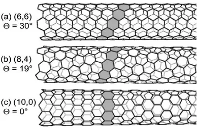
wall of the tube. Single-walled nanotubes having similar diameters show very different microscopic structure due to different chiral angles (figure 2.2).
Figure 2.2 – Three carbon nanotubes with diameters around 0.8 nm: (a) (6,6) armchair, (b) (8,4) chiral tube and (c) (10,0) zigzag nanotube.
Θ is related to the chiral index by
[ ⁄
√ ] [√
]
The chiral angle is allowed to vary between 0° ≤ Θ ≤ 30°; all other ranges of Θ are equivalent to this interval because of the hexagonal symmetry of graphene. A chiral angle of 0° and 30° corresponds to tubes with a particular high symmetry. They are called zigzag (Θ = 0°) and armchair tubes (Θ = 30°). The chiral vector not only determines the tube diameter and chiral angle, but all other structural parameters including the length of the unit cell and the number of carbon atoms in the unit cell.
Figure 2.3 – Chiral indices of single-walled carbon nanotubes mapped onto a graphene sheet. The small symbols at the upper corner of a hexagon indicate the family of a nanotube. Closed circles are semiconducting tubes belonging to the ν = (n1 − n2) mod
3 = −1 (closed circles) or to the ν = (n1 − n2) mod 3 = +1 (open circles). Squares are tubes from the ν = 0 family. These tubes are metallic or quasimetallic, the latter having a small electronic bandgap induced by the curvature of the nanotube wall, ranging
from 10meV to 100meV.
The series of (n, 0) zigzag nanotubes (that run horizontally in figure 2.3) have Θ = 0°. The name derives from the zigzag chain that forms the edge of this high-symmetry type of tubes (see figure 2.2c). The other high-symmetry nanotube structures are the (n, n) armchair tubes with Θ = 30°. The edge of their unit cell resembles a row of armchairs when viewed from above (figure 2.2a), hence the name. Zigzag and armchair tubes are both called achiral tubes. A general nanotube with lower symmetry, like the (8,4) tube in figure 2.2b, is referred to as chiral.
2.3
Electronic Band Structure of Single Walled Carbon Nanotubes
The electronic band structures of single-walled carbon nanotubes (SWNTs) along with their small size and low dimension are responsible for their unique electrical transport properties. Since a SWNT can be considered as a graphene sheet, rolled up to form a hollow cylinder, the band structures of SWNTs can be obtained from that of graphene, a two-dimensional (2D) layer of graphite.
2.3.1 Electronic band structure of graphene
The lattice structure of graphene in real space consists of hexagonal arrangement of carbon atoms. (figure 2.4). An isolated carbon has four valence electrons in 2s, 2px, 2py, and 2pz atomic orbitals. In graphene, three atomic orbitals 2s, 2px, 2py, are hybridized into three sp2 orbitals lying in the same plane while the 2pz orbital remains perpendicular to this plane. The hybridized orbitals are responsible for the bonds between the adjacent carbon atoms and the 2pz orbitals result in bonds out of the plane of graphene. These orbitals lie near the Fermi level and are therefore responsible for the electrical transport properties of graphene.
Figure 2.4 – A graphene sheet, where the carbon atoms are arranged in a honeycomb lattice.
The band structure of graphene derived by orbitals can be calculated by the tight-binding approximation [19]. Graphene unit cell has two nonequivalent carbon atoms, A and B; all other atoms in the lattice can be obtained by translation of A or B using a linear combination of two unit vectors a1 and a2 (figure 2.5a). From the real space lattice is possible to obtain the reciprocal space lattice, characterized by two unit vectors b1 and b2 and by high-symmetry points, , , in a Brillouin zone (figure 2.5b).
Figure 2.5 – Real space representation of a graphene lattice with unit vectors a1 and a2. A unit cell is shown as a dashed rhombus with two carbon atoms (A and B) (a). Reciprocal space representation of a graphene lattice with two unit vectors b1 and b2.
High-symmetry points (Γ, K, M) in a Brillouin zone are also shown (b).
The band structure of graphene orbitals can be obtained resolving Schrödinger equation.
Where H is the Hamiltonian, is the total wave function, and E is the energy of electrons in orbitals of graphene. In a periodic system as in graphene, the total wave function can be constructed from a linear combination of Bloch functions, ui, which has a periodicity of the lattice. In the tight-binding approximation, ui is represented by a linear combination of atomic wave functions. Since only the orbitals from the 2pz orbital of each atom are considered, Bloch function ui, for each atom can be constructed from 2pz orbitals of atoms A and B as
√ ∑
Where X(r) is the orbital 2pz wave function for an isolated carbon atom. Then can be written as:
Leading to: ( ) ( ) ( ) ( )
In which,
〈 | | 〉 〈 | 〉
The overlap between wave functions of different atoms are neglected, i.e. SAB = SBA = 0. Imposing a normalization condition, SAA = SBB = 1, the matrix equation is simplified to:
(
) ( ) ( )
Which has a nontrivial solution only when:
|
|
Since A and B atoms are not distinguishable, HAA = HBB and HAB ≠ HBA, leading to the solution: | |
HAA and HAB can be calculate using the Bloch functions to finally obtain the energy dispersion for orbitals in graphene, using the coordinate system of the graphene in figure 2.5a:
√( (√ ) ( ) ( ))
Where is called as the tight-binding or transfer integral which measures the strength of exchange interaction between nearest atoms. Negative sign denote valence bands of graphene formed by bonding orbitals, while positive sign represents conduction bands formed by antibonding * orbitals. The dispersion relation along high-symmetry points in the reciprocal space with is plotted in figure 2.6.
Figure 2.6 – Energy dispersion of graphene along high-symmetry points
The surface and contour plots of energy dispersion are shown in figure 2.7.
Figure 2.7 –Surface plot (a) and contour plot (b) of the energy dispersion in graphene. There are six K points where the bandgap becomes zero. Of the six K points, only two are nonequivalent, denoted by K1 and K2, originating from two nonequivalent atoms
in the real space unit cell.
The main feature of the energy dispersion of graphene is the six K point at the corners of the Brillouin zone, where the conduction and valence bands meet so that the bandgap is zero only at these points. The density of states (DOS) in graphene can be derived from the energy dispersion relation and it is found to be zero at Fermi level [20]. Along with the zero bandgap, this is why graphene is a zero bandgap semiconductor.
2.3.2 Electronic band structure of SWNTs
A SWNT can be uniquely identified by a chiral vector , where and are integers and and are the unit vectors of the graphene lattice (figure 2.6).
Figure 2.6 – Representation of the chiral vector identifying a (7,1) SWNT.
A SWNT is formed by rolling a graphene sheet so that two carbon atoms pointed by C coincide. The integers and , which are also called wrapping indices, uniquely define and describe a SWNT. SWNTs described by wrapping indices and are called armchair and zigzag SWNTs, respectively.
The band structure of a SWNT can be derived from that of graphene by imposing an appropriate boundary condition around the SWNT. Considering a SWNT as an infinitely long cylinder, there exist two wave vectors associated with it. The wave vector k║, which is parallel to the SWNT axis, is continuous since the SWNT is assumed to be infinitely long, while the wave vector k┴, which is along the circumference of the SWNT, must satisfy a periodic boundary condition, since the wave function repeat itself as it rotates 2 around the SWNT.
This boundary condition can be expressed as:
where d is the diameter of a SWNT and m is an integer. This boundary condition leads to quantized values of allowed for SWNTs. The 1D band structure of SWNTs can be obtained from cross-sectional cutting of the energy dispersion of 2D graphene with these allowed states. This approach is called zone folding scheme and it allows to obtain the band structure of SWNT. Each cross-sectional cutting gives rise to a 1D subband. Therefore, the 1D band structures of SWNTs are determined by the spacing between allowed states and their angles with respect to the surface Brillouin zone of graphene, which is set by the diameter and chirality of SWNTs, i.e. the wrapping indices.
Figure 2. 7 – (a) A first Brillouin zone of graphene with conic energy dispersions at six K points. The allowed k⊥ states in a
SWNT are indicated by dashed lines. The band structure of a SWNT is obtained by cross-sections as indicated. Zoom-ups of the energy dispersion near one of the K points are schematically shown along with the cross-sections by allowed k⊥ states and
resulting 1D energy dispersions for (b) a metallic SWNT and (c) a semiconducting SWNT.
The band structure near the Fermi level, which determines the transport properties, is given by allowed states that are closest to the K points. When the allowed pass directly through the K points (figure 2.7b), the energy dispersion shows two linear bands crossing at the Fermi level without a bandgap. Otherwise, if the allowed states fall far from the K points (figure 2.7c), there are two parabolic 1D bands with an energy bandgap. Therefore, depending on the wrapping indices, SWNTs can have a band structure with or without a bandgap, therefore they can be semiconducting or metallic, respectively.
Considering, as example, the 1D subbands of a zigzag SWNT, described by wrapping indices which can be either metallic or semiconducting; the chiral vector C for a zigzag nanotube is and the boundary condition becomes:
When n is a multiple of 3 ( , where q is an integer), there is an allowed that coincides with a K point, which is at ( ). By substitution,
Then, there is always an integer m ( ) that makes pass through K points so that these zigzag SWNTs (with ) are always metallic without a bandgap.
There are two cases when n is not a multiple of 3. If , the closest to K point is at :
Similarly, for , the allowed closest to K is when :
In these two cases, allowed misses K points by:
The smallest misalignment between an allowed and a K point is inversely proportional to the diameter. Then, the bandgap is given by:
(
) ( )
Therefore, semiconducting SWNTs (d = 0.8 – 3 nm ) have a bandgap in the order of 0.2 – 0.9 eV, inversely proportional to the diameter. Similar treatment for armchair SWNTs (n, n) leads to the conclusion that they are always metallic.
Using wrapping indices , SWNTs can be classified into three different categories depending on the value of p, which is the remainder when the difference between wrapping indices is divided by 3 (i.e. ):
(i) p = 0; metallic with linear subbands crossing at the K points (ii) p = 1, 2; semiconducting with bandgap, Eg 0.7 eV/d (nm)
2.3.3 Deviation from simple tight-binding zone folding scheme
In the zone-folding derivation of the electronic band structure of SWNTs, nanotubes are treated as graphene sheet with a periodic boundary condition with the assumption that orbitals are still orthogonal to orbitals in the graphene plane so that orbitals can be treated independently as in the graphene case. This assumption is not valid for SWNTs because their curvature mixes and orbitals, leading to the hybridization between these orbitals, with the degree of hybridization becoming larger as
the diameter of SWNT gets smaller. The main result of this - hybridization is to open a small bandgap in metallic SWNTs, with the exception of the armchair nanotubes due to symmetry (figure 2.8). This is a secondary effect as the bandgap goes as , ranging from a few meV to tens of meV for a diameter of 3 nm or smaller.
Figure 2.8– The calculated curvature-induced bandgaps for metallic SWNTs. The bandgap is still zero for armchair SWNTs.
2.3.4 Density of States in SWNTs
The DOS is an actual physical quantity that can be measured with different techniques as scanning tunneling microscopy, electrical transport measurements, and optical measurements (photoluminescence). The DOS, n(E), with 1D subbands (k) can be calculate as:
∑ ∫ | |
Where ki are the roots of the equation , l is the length of the 1D Brillouin zone, and N(E) is the total number of electron states per unit cell below a given energy E. For parabolic 1D subbands such as those of semiconducting SWNTs (figure 2.7c), the resulting DOS is proportional to ⁄ for each subband and diverges for each onset of a subband, giving rise to the so-called van Hove singularity in 1D systems. In higher dimensionality system DOS goes to zero with ⁄ in 3D and over series of step at each inset of a subband in 2D systems (figure 2.9).
Figure 2.9 – Density of states in systems with different dimensions.
The metallic bands at K points can be approximated by a linear dispersion (figure 2.7b), so they lead to finite, constant DOS.
For SWNTs the equation can be solved as
√ ∑ Where { | | √ | | | | | | | |
becomes divergent whenever , corresponding to van Hove singularity and . These leads to different 1D density of states for semiconducting and metallic SWNTs (figure 2.10).
Figure 2.10 – The electronic density of states for a (a) (10, 0) semiconducting and (b) (9, 0) metallic SWNT. Dotted lines are for the density of states of graphene (which is zero at the Fermi level).
While DOS is zero at K points in graphene, it is finite for metallic SWNTs, due to the 1D characteristics of SWNTs. Zero bandgap and finite DOS at the Fermi level entitles metallic SWNTs as truly metallic, unlike graphene.
2.4
Electron Transport
in Single Walled Carbon Nanotubes
Resistance in solid system is due to the scattering of charge carriers as they travel through the system. In solid state system, main sources of scattering are static defects (imperfection, impurities…) and phonons (lattice vibrations). Usually, scattering of phonons is dominant at high temperature while impurity scattering prevails at low temperatures. In SWNTs there are various sources of carrier scattering affecting transport characteristics.
2.4.1 Scattering in SWNTs
Charge carrier scattering in 1D system is quite different from the one in higher dimensions because carriers can only forward or backward scatter while in higher dimension they can be scattered into many different directions.
In general there are two types of scattering processes in solid systems: one is the scattering by static potentials such as impurities which does not change the energy of the particles being scattered; the other is the scattering by time-varying potential such as phonons which results in inelastic scattering with energy as well as momentum changes.
Scattering by defects or impurities is due to scattering potentials which are generally static in time. The scattering potential can be a screened or unscreened Coulomb neutral defect. Although SWNTs retain high crystallinity, they inevitably have different kinds of structural defects such as vacancies or pentagon-heptagon pairs and impurities such as foreign atoms or chemicals deposited in the surface. Despite these imperfections, metallic SWNTs are expected to have a long mean free path, even at room temperature, and this is attributed to the suppressed back scattering due to high symmetry of SWNTs, especially armchair SWNTs. Metallic SWNTs have two degenerate 1D subbands crossing at the Fermi level. Each subband corresponds to a different moving direction for electrons and backscattering requires electrons move from one subband to the other. Due to symmetry, these two crossing 1D subbands are orthogonal to each other and do not mix resulting in a significant suppression of backscattering in metallic SWNTs. As long as the defects do not significantly perturb the band symmetry of SWNTs, metallic SWNTs have a large mean free path. Defects such boron and nitrogen impurities and pentagon-heptagon pairs are expected to affect the electrical transport properties of metallic SWNTs, but only far away from the Fermi level, while vacancies which have a short range potential seem to affect the transport near the Fermi level.
As scattering due to defects are suppressed in SWNTs, the main source of scattering is believed to be phonons, especially at high temperatures. Various phonon modes exist in SWNTs (figure 2.11).
Figure 2.4 – Phonon dispersion relation of graphene
Phonon scattering is an inelastic scattering process which requires the momentum and energy conservations by electrons and phonons combined. Limited momentum space of SWNTs along with the symmetry requirements leave only three possible electron-phonon processes satisfying the momentum and energy conservations (figure 2.12).
Figure 2.5 – Allowed electron backscattering process in a metallic SWNT by (a) acoustic phonons, (b) optical phonons, and (c) zone boundary phonons with energy
The first one is scattering by low energy acoustic phonons which involves a small momentum and energy changes. The other two scattering process are due to the high energy optical and zone boundary phonons which require large energy changes (150-180 meV) with small and large momentum, respectively. Phonon scattering involves either emission or absorption of the phonons by traveling charge carriers.
At low electric field acoustic phonon scattering (a) is the only available scattering process since electrons do not have enough energy to interact with the high-energy phonons. In this regime, resistance is inversely proportional to the temperature since the scattering rate is determined by number of phonons available and the occupation of acoustic phonons is proportional to the temperature. Due to their high energy, compare to the room temperature, kBT 25 meV, the optical and zone boundary phonons are not expected to be present at room temperature so that the scattering in this case corresponds to only the emission of phonons by electrons.
At high electric fields, electrons can acquire enough energy to emit optical and zone boundary phonons, which results in the backscattering of electrons. As long as the mean free path for high energy phonon scattering is much smaller than the SWNT length, it can be assumed that electrons backscatter instantly when they acquire enough energy to emit high-energy phonons.
2.5
Optical Properties of Single Walled Carbon Nanotubes
Optical properties of single-walled nanotubes are governed by the extended -electron system. The available electronic states in such -system reflect the unusual band structure of nanotubes which varies with the (n,m) values describing each nanotube’s structure, meaning that each physical SWNT structure has its own characteristic electronic structure. The diversity of electronic properties and their strong dependence on nanotube structure constitute one of the most remarkable and potentially useful features of SWNTs, which must be viewed as a family of related materials rather than a single substance such as C60.
SWNTs for which n = m have a finite density of states at the Fermi energy and display metallic electronic behavior. Other structures for which the quantity (n–m) is evenly divisible by 3 are semimetallic, with band gaps smaller than kBT at room temperature, whereas SWNT in which (n–m) does not divide evenly by 3, are semiconductors with their bandgap varying approximately inversely with nanotube diameter. Nanotubes with the same (n,m) identity but different lengths have matching optical and electronic properties because SWNT electronic structure is governed by transverse structure. The quasi-one-dimensionality of nanotubes has an important electronic consequence for all (n,m) species: it introduces sharp spikes, called van Hove singularities, into the densities of states (figure 2.13).
Figure 2.63 –Schematic density of states diagram for a semiconducting single-walled carbon nanotube, in a simple band theory model. Allowed optical transitions are illustrated as vertical arrows.
Figure 2.13 shows a band theory model density of states function for a semiconducting SWNT [21]. Each van Hove singularity belongs to a different sub-band. Optical absorption and emission are dominated by dipole-allowed transitions in which light polarized with its electric vector parallel to the tube axis promotes an electron from a valence subband to the corresponding conduction sub-band, conserving the angular momentum projection. In a one-electron model, these transitions are predicted to be most intense when the photon energy matches the energy difference between corresponding van Hove singularities. The absorption and emission spectra of a single (n,m) species of SWNT are therefore expected to consist mainly of a series of sharp features at energies Eii, where i takes the values 1, 2, 3, according to subband.
2.5.1 Absorption of SWNTs
For semiconducting SWNTs with diameters near 1 nm, the first three of these transitions will appear in the near-infrared, visible, and near-ultraviolet regions. Metallic or semimetallic SWNTs of similar diameter have their lowest energy optical transitions at visible wavelengths falling between the semiconducting nanotubes’ E22 and E33 features. In addition, semimetallic nanotubes also have much lower energy absorptions in the far-infrared at wavelengths near 100 mm [22,23]. These correspond to transitions across the small, diameter-dependent band gaps (in the range of 10 meV) that are induced by s–p hybridization associated with the nanotubes’ cylindrical curvature [24]. Apart from the nondispersive interband optical transitions in the infrared and visible that are characteristic of nanotube diameter and chiral angle, SWNT samples also display dispersive, intense near-ultraviolet absorptions at 4.5 and 5.2 eV that have been assigned to collective plasmon excitations of their p-electrons [25,26]. The near-infrared and visible transitions of SWNTs would be expected to be quite useful in distinguishing different structural species from one another. However, it was found that spectra of samples containing many species typically showed broad, undifferentiated optical absorption features arising from strongly overlapped transitions of those species, rather than sharp, resolved absorptions. In addition, no emission was observed that could be assigned to van Hove interband transitions.
A breakthrough in nanotube spectroscopy occurred with the 2002 report of structured absorption from samples of SWNTs that had been prepared with special processing to counteract their strong tendency to form bundles of parallel nanotubes held together by van der Waals forces [27]. To obtain these disaggregated samples, raw and unpurified product from the HiPco process was first mechanically dispersed into an aqueous solution of a surfactant such as SDS (sodium dodecylsulfate). Then intense ultrasonic agitation was applied to free many individual nanotubes from bundles. Once freed, the nanotubes became surrounded by a micelle-like layer of surfactant molecules that prevented their reaggregation into bundles. Finally, the sample was subjected to ultracentrifugation, which allowed significant physical separation of suspended individual nanotubes from the slightly denser suspended bundles. Decanted portions of such processed samples showed notably complex and sharpened near-infrared absorption spectra with structure extending from approximately 900 to 1600 nm (figure 2.14). D2O was used in preference to H2O as the solvent for spectroscopic studies because of its superior
near-infrared transparency. The isotopic frequency shift of the O–H stretching overtone increases the long wavelength cut-off of D2O to ca. 1900 nm from 1350 nm in H2O.
Figure 7.14 – Optical absorption spectrum of a sample of HiPco single-walled carbon nanotubes suspended in D2O by SDS surfactant at 276 K.
2.5.2 Emission of SWNTs
These aqueous samples enriched in individual surfactant-suspended SWNTs also displayed near-infrared photoluminescence with highly structured emission spectra showing a series of peaks nearly coincident with those in the absorption spectrum (figure 2.15). The emission red-shifts are only approximately 4 meV (30 cm_1).
Figure 2.15 – Absorption and emission spectra of a sample of HiPco nanotubes in SDS/D2O suspension. The emission was excited by a pulsed laser at 532 nm.
This similarity of absorption and emission spectra differs strikingly from the ‘‘mirror-image’’ relation that is common in molecular photophysics. The data show that the sample contains many emitting species, with each displaying one dominant transition in this spectral range and a very small Stokes shift between its absorption and emission peaks. In accord with the predictions of Kasha’s Rule that molecular electronic luminescence originates entirely from the lowest-lying electronic state within a spin multiplicity manifold [28], SWNT emission is observed exclusively for E11 transitions and not for E22 or higher transitions. Clearly, the many distinct spectral features in the E11 region correspond to different (n,m) species of semiconducting single-walled nanotubes in the structurally heterogeneous sample. Precise values of photoluminescence quantum yields are difficult to measure, in part because of overlapping transitions in mixed samples. However, initial estimates suggest quantum yields that are near 10-3 and vary somewhat as the nanotube’s environment is altered by the presence of different surfactants. Lifetime studies on SWNT optically excited states have been reported by several laboratories [29–31]. The excited state lifetime of ca. 10-10 s can be combined with the emissive quantum yield near 10-3 to deduce that the emitting state has a radiative rate constant consistent with a spin-conserving optical transition. Using the terminology of molecular photophysics, nanotube photoluminescence is therefore classified as fluorescence rather than phosphorescence.
Only semiconducting SWNTs emit fluorescence, because the nonzero density of states in metallic species causes non radiative recombination of the photoinduced excitons (figure 2.16).
Figure 2.16 – Schematic density of electronic states for a single nanotube structure. For semiconducting species (left), excitation is followed by fluorescence upon phonon relaxation (dashed arrows). For metallic species (right), excitation is followed by non
radiative decay because of the non-zero density of states at the Fermi level.
The near infrared emission due to a fluorescent bandgap transition can therefore be used for the identification of the specific nanotubes structure responsible for each peak. This was obtained using spectrofluorimetry, reporting the measured emission intensity as a function of two variables: excitation and emission wavelength. The excitation source’s wavelength was scanned over the range of E22 transitions, and when the photon energy matched the second van Hove transition energy of one of the
SWNT species in the sample, the resulting optical absorption generated a hole in its second valence sub-band and an electron in its second conduction sub-band. The electrons and holes relaxed through phonon emission to the first sub-bands. Then a small fraction of the excited nanotubes emitted E11 near-infrared fluorescence through radiative electron–hole recombination across the semiconducting band gap. The wavelength of this emission was characteristic of the nanotube species that had undergone resonant E22 excitation.
Figure 2.17 – Surface plot showing emission intensity from a sample of HiPco SWNT in SDS/D2O suspension as a function of excitation and emission wavelengths. Each distinct peak arises from a specific (n,m) species of semiconducting nanotube.
The results from this experiment can be summarized in the form of a surface plot, where height corresponds to emission intensity and the two other axes represent excitation and emission wavelengths (figure 2.17). A rich structure of ‘‘mountain peaks’’ is clearly evident for excitation in the E22 range between ca. 500 and 800 nm. Each of these peaks arises from a distinct (n,m) species of semiconducting nanotube. The unique E11 and E22 transition energies of each species may be simply found from the wavelength coordinates of its peak, providing a valuable correlation of E11 and E22 values for many different nanotube species.
Fluorescence is the optical property of nanotubes that is most sensitive to sample condition. The absence of near-IR emission from nanotubes that have aggregated into bundles held together by van der Waals forces seems likely to arise from efficient energy transfer within the bundle. Statistically, approximately one-third of the nanotubes in a raw sample are expected to be metallic. There is therefore a high probability that randomly formed bundles containing at least several nanotubes will include one or more metallic tubes. When a bundled semiconducting SWNT absorbs light, electronic coupling with its neighbors causes excitation transfer to species with smaller band gaps and eventually
to a metallic nanotube, in which the excitation must relax nonradiatively. This efficient fluorescence quenching process allows one to use emissive yield as a sensitive monitor of SWNT aggregation. Fluorescence efficiency can also be sensitive to chemical environment. The addition of acid to aqueous suspensions of pristine SWNT in ionic surfactants causes fluorescence quenching that can be reversed by the addition of base to restore pH to a neutral or alkaline value [32–34]. Such quenching differs from the complete and essentially irreversible loss of near-infrared fluorescence caused by many oxidative acid treatments that are commonly applied to raw SWNT material to remove residual metallic catalysts. In addition, many chemical reactions that derivatize nanotube sidewalls inhibit fluorescence. It seems likely that the perturbation of a nanotube’s -electron system by the chemical conversion of functionalized carbon atoms from sp2 to sp3 hybridization produces sites for efficient nonradiative recombination of excitons. Although such chemical derivatization also leads to the characteristic D-band in Raman spectra and the loss of van Hove structure in electronic absorption spectra, fluorescence is lost significantly before the onset of these other spectroscopic symptoms. This high sensitivity of fluorescence quantum yield to sidewall defects may reflect the mobility of excitons along the tube axis. Through such motion the electronic excitation can visit relatively large segments of a nanotube during its lifetime and undergo efficient quenching by sparse defect sites.
2.6
Raman Spectroscopy of Single Walled Carbon Nanotubes
Raman spectra of SWNTs contain many features that can be identified with specific phonon modes and with specific Raman scattering processes that contribute to each feature. The Raman spectra of SWNTs can therefore provide much information about 1D properties, such as their phonon structure and their electronic structure, as well as information about sample imperfections (defects). Since mechanical properties, elastic properties and thermal properties also are strongly influenced by phonons, Raman spectra provide much general information about the structure and properties of SWNTs.
2.6.1 Phonon structure
Phonons denote the quantized normal mode vibrations that strongly affect many processes in condensed matter systems, including thermal, transport and mechanical properties.
Figure 2.18 – (a) Phonon dispersion of 2D graphite [35]. (b) The phonon density of states for a 2D graphene sheet. (c) The calculated phonon dispersion relations of an armchair carbon nanotube with (n, m) = (10, 10), for which there are 120 degrees of
freedom and 66 distinct phonon branches [17], calculated from (a) by using the zone folding procedure. (d) The corresponding phonon density of states for a (10,10) nanotube.
The 2D graphene sheet has 6 phonon branches, as shown in figure 2.18a. Since the SWNTs can be considered to be a 2D graphene sheet that has been rolled up seamlessly, a similar folding procedure, as was used for describing the electronic structure, is generally applied to obtain the phonon dispersion relations and phonon density of states for SWNTs from those of the 2D graphene sheet [17].
The phonon dispersion for a (10,10) SWNT obtained by this folding procedure is illustrated in figure 2.18 c, and the respective phonon DOS is shown in figure 2.18d. The large amount of sharp structure in the phonon density of states in figure 2.18d for the (10,10)SWNT reflects the many phonon branches and the 1D nature of SWNTs relative to 2D graphite arising from the quantum confinement of the phonon states into van Hove singularities. The phonon density of states for 2D graphite is shown in figure 2.18b for comparison.
2.6.2 Raman Scattering Process
Raman scattering is the inelastic scattering of light. During a scattering event, (1) an electron is excited from the ground level to a virtual excited state by absorbing a photon, (2) the excited electron is scattered by emitting (or absorbing) phonons, and (3) the electron relaxes to the ground level by emitting a photon. Raman scattering can occur for phonon emission or by phonon absorption, and these two processes are called the Stokes process and anti-Stokes process, respectively. If light scattering occurs elastically, i.e. change of photon direction but no frequency shift, the process is called Rayleigh scattering (figure 2.19).
Figure 2.19 – Elastic and inelastic light scattering giving Rayleigh and Raman scattering , respectively.
Raman spectra generally report the scattered photon (light) whose energy is smaller by the phonon energy than that of the incident photon, i.e. Stokes scattering. By measuring the intensity of the scattered light as a function of frequency downshift (losing energy) of the scattered light, an accurate measure of the phonon frequencies of the material is obtained.
2.6.3 Resonance and non-resonance Raman scattering
When the energy separation between the ground and excited states is not equal to the photon energy and photon absorption process occurs through a final virtual state, the transition is called a virtual transition and the Raman process is non-resonant.
When the optical absorption (or emission) is to (or from) a real electronic state, the transition is resonant and its scattered amplitude becomes very large, giving a resonant Raman scattering.
Figure 2.20 – Incident resonance (left) and scattered resonance (right) processes.
There are two resonance conditions for optical transitions: resonance with the incident laser photon (incidence resonance) and resonance with the scattered photon (scattered resonance) (figure 2.20). When the resonance occurs with the incident photon, the incident laser light has the same energy (EL) as the energy separation between the two electronic states in resonance (Eii)
EL = Eii In this case, all Raman features are resonantly enhanced.
When the resonance occurs with the scattered photon, the incident laser light has the same energy (EL) as the energy separation between the two electronic states in resonance (Eii), with an additional energy of the phonon ωi.
EL = Eii + ωi
In this case the resonance condition depends on the phonon energy ωi.
Thus in the Stokes Raman process, the shift in the resonant energy for the scattered resonance state is larger than that for incident resonance state by the phonon energy.
Non-resonant Raman spectra are much weaker in intensity than resonance Raman spectra. The resonance Raman process increases the signal by a factor of approximately 103 in comparison to the intensity for a non-resonance Raman process. In the case of SWNTs, not only resonant enhancement but also a singularity in the DOS contributes to the Raman intensity. When the laser energy of either the incident or the scattered light has the same energy as a van Howe singularity energy in the JDOS, the Raman intensity becomes extremely strong for any SWNT that satisfies the resonance condition. This is the reason why it is possible to get a measurable signal from a single isolated SWNT in the presence of many non-resonant (n, m) SWNTs.
2.6.4 Classification of Raman scattering processes
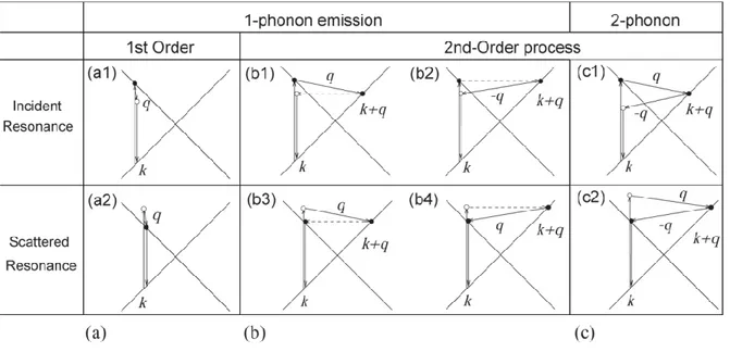
The number of emitted phonons before relaxation of the lattice can be one, two, and so on, giving, respectively, one-phonon, two-phonon and multi-phonon Raman processes. The order of a scattering event is defined as its number in the sequence of the total scattering events, including elastic scattering by an imperfection (such as a defect or edge) of the crystal.
Figure 2. 21 – (a) First-order and (b) one-phonon second-order, (c) two-phonon second-order, resonance Raman spectral processes. (top) incident photon resonance and (bottom) scattered photon resonance conditions. For one-phonon, second-order
transitions, one of the two scattering events is an elastic scattering event (dashed lines). Resonance points are shown as solid circles.
The lowest order process is the first-order Raman scattering process which gives Raman spectra involving one-phonon emission (figure 2.21a). In order for an electron to recombine with a hole, the scattered k + q states should not differ from k by more than two times the photon wave vector.
In second-order Raman scattering, q and −q scattering wave vectors are involved, so that an electron can return to its original k position after scattering. The electron absorbs a photon at a k state, scatters to k + q states, scatters back to a k state, and emits a photon by recombining with a hole at a k state. The two scattering processes consist of either elastic scattering by defects of the crystal or inelastic scattering by emitting a phonon, characterizing, respectively, one- and two-phonon double-resonance Raman process.
Second-order Raman scattering consists of one-phonon and one elastic scattering event (figure 2.21b) or two-phonon scattering events (figure 2.21c). In the case of two-phonon scattering events, it can be involved the same phonon modes (overtone mode) or different phonon modes (combination mode).
2.6.5 Raman spectra of SWNTs
Raman spectra of SWNTs are characterized by many features that can be identified with specific phonon modes and with specific Raman scattering processes (figure 2.22).
Figure 2.22 – Raman spectrum of a HiPco SWNTs
In SWNTs, the G-band spectra, which is split into many features around 1580 cm−1, and the lower frequency radial breathing modes (RBMs) are usually the strongest features in SWNT Raman spectra, and are both first-order Raman modes. The D-band at 1350 cm−1 and the G’-band at 2700 cm−1 (for EL
= 2.41 eV) are, respectively, due to one- and two-phonon, second-order Raman scattering processes.
2.6.5.1 Radial Breathing Modes
The radial breathing mode (RBM) Raman features is a totally symmetric vibrational mode associated with the coherent vibration of the C atoms in the radial direction with respect to the nanotube axis (figure 2.23).
These features are unique to carbon nanotubes and occur with frequencies (ωRBM) between 120 and 350 cm-1 for SWNTs with diameter in the range 0.7 nm < dt < 2 nm. Theoretical and experimental results show that the ωRBM is inversely proportional to the nanotube diameter dt but does not depend on the chiral angle of the tubes. These RBM frequencies are therefore useful for verifying the presence of SWNTs through the presence of RBM modes and for characterizing the nanotube diameter distribution in the sample through the relation:
ωRBM = A/dt + B
where A and B parameters are determined experimentally [36,37]. (B is an upshift in ωRBM assigned to tube-tube interactions). For typical SWNT bundles in the diameter range dt = 1.5 ± 0.2 nm, A = 234 cm-1 and B = 10 cm-1 has been found [37]. For dispersed SWNTs in aqueous solution, A = 239, B = 0. For isolated SWNTs on an oxidized Si substrate, A = 248 cm-1 and B = 0 has been found [36,38]. These two set of values of A and B give similar dt for a given ωRBM only if the diameter is comprised between 1 a 2 nm. When dt < 1 nm, the distortions of nanotube lattice lead to a chirality dependence of ωRBM. For dt > 2 nm the intensity of RBM features is weak and difficult to observe. Therefore, from the ωRBM measurement of an individual isolated SWNT, it is possible to obtain a value of its diameter dt. The RBM spectra for SWNT bundles contain an RBM contribution from different SWNTs in resonance with the excitation laser line.
Single Raman measurement gives an idea of the tubes that are in resonance with the laser line, but does not give a complete characterization of the diameter distribution of the sample. A good characterization of the diameter distribution can be obtained taking Raman spectra using many laser lines. Since semiconducting and metallic tubes of similar diameter do not occur at similar Eii values, ωRBM measurement using several EL can be used to characterize the ratio of metallic to semiconducting SWNT in a given sample.
2.6.5.2 G-band
The G-band involves an optical phonon between the two dissimilar carbon atoms A and B in the unit cell and it is common to all sp2 carbon system. In graphite G-band shows one single Lorentzian peak at 1582 cm-1 whereas SWNTs G-band is composed of several peaks because of the phonon wave vector confinement along the SWNT circumferential direction and due to symmetry-breaking effects associated with SWNT curvature. The G-band frequency can be used for diameter characterization, to distinguish between metallic and semiconducting SWNTs, through strong differences in their Raman lineshapes.
Figure 2.24 – Tangential and circumferential vibration modes responsible of G-band splitting in SWNTs.
G-band feature for SWNTs consists of two main components, one peaked at 1590 cm-1 (G+) and the other peaked at about 1570 cm-1 (G-). The G+ feature is associated with carbon atom vibrations along the nanotube axis while the G- feature, in contrast, is associated with vibrations of carbon atoms along the circumferential direction of the SWNT (figure 2.24).
For individual semiconducting SWNTs, both features exhibit a Lorentzian lineshape. The position of the higher energy component G+ is almost independent of diameter, whereas the lower energy component G- shows a clear diameter dependence, where the wavenumber of the mode decreases with decreasing tube radius. For metallic tubes, the G- component is widely broadened and asymmetric. This broadening is commonly attributed to a Breit-Wigner-Fano (BWF) resonance of metallic SWNTs induced by a coupling of the phonon excitation to a continuum of plasmon states (figure 2.25).
Experimentally, it was shown that the intensity of the BWF component exhibits a diameter dependence as well [39] (figure 2.26).
Figure 2.26 – Frequency vs. 1/dt for the two G-band features (G+ and G-) from isolated SWNTs
For an ensemble of metallic and semiconducting SWNTs, the resonance condition determines the lineshape of the G- component. If, for a given diameter distribution, the excitation energy probes predominantly metallic SWNTs, an asymmetric BWF component is observed in contrast to photon energies where excitations of semiconducting SWNTs prevail.
2.6.5.3 D-Band
Disorder-induced (or defect-induced) D-band is the most common example of a second-order feature in the Raman spectra of SWNTs. This band is usually observed between 1300-1400 cm-1. The D band is common to all sp2-hybridized disordered carbon materials. In SWNTs D-band becomes active because of the presence of defects, such as impurities, missing atoms or sp3-hybridized functionalized carbon atom on SWNT sidewalls. The D-band frequency ωD shows a strong dependence on the excitation laser energy. This dispersive behavior is explained through a double-resonance process where the electron after being promoted because of photon absorption, is scattered by a phonon and elastically scattered
back by a defect, or vice versa, then recombining with the previously created hole and finally emitting a scattered photon.
D-band is commonly used for a qualitatively defect characterization because it is known to originate from defects but until now there is no correlation between D-band and the different type of defects such as hetero-atoms, vacancies, heptagon-pentagon pairs, kinks, or other impurities [40].
Isolated SWNTs exhibit different ωD values for a given EL, because the double resonance condition must be satisfied for each tube. Therefore, D-band for a sample composed of an ensemble of nanotubes is the sum of different features originating from different (n, m) species of nanotubes and for
resonances with different Eii. A diameter dependence of ωD is also observed, with ωD decreasing with decreasing diameter (1/dt dependence). In isolated SWNTs, a large D peak compared to the G peak usually indicates a bad resonance condition, which is EL is not close to Eii. In SWNT bundles a large D-band indicates the presence of amorphous carbon. D features correlated to isolated nanotubes have usually small linewidths, between 40 and 7 cm-1, while amorphous carbon is responsible of a broad feature.
2.6.5.4 G’-band
The G’-band is the second harmonic of the D-band, occurring at 2ωD ( 2700 cm-1) because the electron is backscattered by a second phonon instead than of a defect, leading to a two-phonon, second-order Raman scattering processes. So defect are no longer necessary and G’-band is present even in defect-free nanotubes for which the D band is completely absent. As for D-band, the G’-band is sensitive to the SWNTs diameter and chirality, so measurement on isolated nanotubes allow the assignment of the indices (n, m).
2.6.5.5 D/G Ratio
Changes in the D-band Raman spectra can be used for SWNTs characterization to probe and monitor structural modifications of the nanotube sidewalls like the introduction of defects. Sample purity is traditionally investigated by comparing the amplitude of the D mode to that of the G mode [41,42], which, as a first-order process, is supposed to be independent of defect density. Therefore the D/G band intensity ratio in SWNTs Raman spectra is conventionally used as an average estimation of sample’s defects, including the presence of amorphous carbon and defects like vacancies or functional groups covalently attached on nanotube sidewalls.
2.7
Synthesis of Single Walled Carbon Nanotubes
The most widely used techniques for SWNTs are: arc-discharge, laser ablation and synthesis by chemical CVD. SWNTs can only be grown with a catalyst. Transition metal (Fe, Co, Ni) are the most commonly used catalyst for SWNTs growth. The detailed mechanism responsible for growth are not yet well understood but the width and peak of the diameter distribution depends on the composition of the catalyst, the growth temperature and various other conditions.
2.7.1 Arc-Discharge
The arc-discharge method creates nanotubes through arc-vaporization of two carbon-rod electrodes, separated distant 1 mm from each other, in inert atmosphere (helium or argon) at low pressure (between 50 and 700 mbar) (figure 2.27). A direct current (from 50 to 100 A at 20 V) creates a high temperature discharge between the two electrodes. The discharge vaporizes one of the carbon rods and forms a deposit on the other rod. Nanotubes self-assemble from the resulting carbon vapor. The arc-discharge method yields highly graphitized tubes with structural perfection, because of the very high process temperature around 3000°C. In order to produce SWNTs, the graphite-rod anode has to be doped with metal catalyst. The yield of the process depends strongly on the uniformity of the plasma arc and the temperature of the deposit on the carbon electrode. The arc-discharge method creates also a large amount of by-products, mainly carbonaceous materials, such as amorphous carbon, nanoparticles and fullerenes, which need to be removed in post-synthesis purification processes.