Nonlinear optical response of low loss silicon
germanium waveguides in the mid-infrared
L. Carletti,1,* P. Ma,2 Y. Yu,2 B. Luther-Davies,2 D. Hudson,3 C. Monat,1 R. Orobtchouk,1 S. Madden,2 D. J. Moss,4 M. Brun,5 S. Ortiz,5 P. Labeye,5 S. Nicoletti,5
and C. Grillet1
1University of Lyon, Institut des Nanotechnologies de Lyon, Ecole Centrale de Lyon, 36 Avenue Guy de Collongue,
69134 Ecully, France
2CUDOS, Laser Physics Centre, Australian National University, Canberra, ACT 0100, Australia 3CUDOS, School of Physics, University of Sydney, NSW 2006, Australia
4School of Electrical and Computer Engineering, RMIT University, Melbourne, Victoria 3001, Australia 5CEA-Leti MINATEC Campus, 17 rue des Martyrs 38054 GRENOBLE Cedex 9, France
Abstract: We have investigated the nonlinear optical response of low loss Si0.6Ge0.4 / Si waveguides in the mid-infrared wavelength range from 3.25-
4.75μm using picosecond optical pulses. We observed and measured the three and four-photon absorption coefficients as well as the Kerr nonlinear refractive index. The dynamics of the spectral broadening suggests that, in addition to multiphoton absorption, the corresponding higher order nonlinear refractive phenomena also needs to be included when high optical pulse intensities are used at mid-infrared wavelengths in this material.
©2015 Optical Society of America
OCIS codes: (190.4390) Nonlinear optics, integrated optics; (190.4400) Nonlinear optics,
materials; (230.3120) Integrated optics devices; (130.2790) Guided waves; (130.3060) Infrared. References and links
1. B. Jalali, “Nonlinear optics in the mid-infrared,” Nat. Photonics 4(8), 506–508 (2010).
2. R. Soref, “Mid-infrared photonics in silicon and germanium,” Nat. Photonics 4(8), 495–497 (2010). 3. J. Leuthold, C. Koos, and W. Freude, “Nonlinear silicon photonics,” Nat. Photonics 4(8), 535–544 (2010). 4. C. Monat, C. Grillet, M. Collins, A. Clark, J. Schroeder, C. Xiong, J. Li, L. O’Faolain, T. F. Krauss, B. J.
Eggleton, and D. J. Moss, “Integrated optical auto-correlator based on third-harmonic generation in a silicon photonic crystal waveguide,” Nat. Commun. 5, 3246 (2014).
5. B. Corcoran, C. Monat, C. Grillet, D. J. Moss, B. J. Eggleton, T. P. White, L. O. Faolain, and T. F. Krauss, “Green light emission in silicon through slow-light enhanced third-harmonic generation in photonic- crystal waveguides,” Nat. Photonics 3(4), 206–210 (2009).
6. C. Grillet, L. Carletti, C. Monat, P. Grosse, B. Ben Bakir, S. Menezo, J. M. Fedeli, and D. J. Moss, “Amorphous silicon nanowires combining high nonlinearity, FOM and optical stability,” Opt. Express 20(20), 22609–22615 (2012).
7. X. Liu, R. M. Osgood, Jr., Y. A. Vlasov, and W. M. J. Green, “Mid-infrared optical parametric amplifier using silicon nanophotonic waveguides,” Nat. Photonics 4(8), 557–560 (2010).
8. G. Z. Mashanovich, M. M. Milošević, M. Nedeljkovic, N. Owens, B. Xiong, E. J. Teo, and Y. Hu, “Low loss silicon waveguides for the mid-infrared,” Opt. Express 19(8), 7112–7119 (2011).
9. P. Y. Yang, S. Stankovic, J. Crnjanski, E. J. Teo, D. Thomson, A. Bettiol, M. B. H. Breese, W. Headley, C. Giusca, G. T. Reed, and G. Z. Mashanovich, “Silicon photonic waveguides for mid- and long-wave infrared region,” J. Mater. Sci. Mater. Electron. 20(S1), 159–163 (2009).
10. B. Kuyken, X. Liu, R. M. Osgood, Jr., R. Baets, G. Roelkens, and W. M. J. Green, “Mid-infrared to telecom-band supercontinuum generation in highly nonlinear silicon-on-insulator wire waveguides,” Opt. Express 19(21), 20172–20181 (2011).
11. R. Shankar, I. Bulu, and M. Lončar, “Integrated high-quality factor silicon-on-sapphire ring resonators for the mid-infrared,” Appl. Phys. Lett. 102(5), 051108 (2013).
12. X. Gai, Y. Yu, B. Kuyken, P. Ma, S. J. Madden, J. Van Campenhout, P. Verheyen, and R. Baets, “Nonlinear absorption and refraction in crystalline silicon in the mid-infrared,” Laser Photonics Rev. 7, 1–11 (2013). 13. M. Muneeb, X. Chen, P. Verheyen, G. Lepage, S. Pathak, E. Ryckeboer, A. Malik, B. Kuyken, M. Nedeljkovic,
J. Van Campenhout, G. Z. Mashanovich, and G. Roelkens, “Demonstration of Silicon-on-insulator mid-infrared spectrometers operating at 3.8 μm,” Opt. Express 21(10), 11659–11669 (2013).
14. C. Grillet, P. Ma, B. Luther-Davies, D. Hudson, C. Monat, S. Madden, D. J. Moss, M. Brun, P. Labeye, S. Ortiz, and S. Nicoletti, “Low loss SiGe waveguides in the MID-IR,” in 2013 Conference on Lasers and Electro-Optics
15. M. Brun, P. Labeye, G. Grand, J. M. Hartmann, F. Boulila, M. Carras, and S. Nicoletti, “Low loss SiGe graded index waveguides for mid-IR applications,” Opt. Express 22(1), 508–518 (2014).
16. N. K. Hon, R. Soref, and B. Jalali, “The third-order nonlinear optical coefficients of Si, Ge, and Si1−xGex in the midwave and longwave infrared,” J. Appl. Phys. 110(1), 011301 (2011).
17. K. Hammani, M. A. Ettabib, A. Bogris, A. Kapsalis, D. Syvridis, M. Brun, P. Labeye, S. Nicoletti, D. J. Richardson, and P. Petropoulos, “Optical properties of silicon germanium waveguides at telecommunication wavelengths,” Opt. Express 21(14), 16690–16701 (2013).
18. K. Hammani, M. A. Ettabib, A. Bogris, A. Kapsalis, D. Syvridis, M. Brun, P. Labeye, S. Nicoletti, and P. Petropoulos, “Towards nonlinear conversion from mid- to near-infrared wavelengths using Silicon Germanium waveguides,” Opt. Express 22(8), 9667–9674 (2014).
19. P. Ma, D. Y. Choi, Y. Yu, X. Gai, Z. Yang, S. Debbarma, S. Madden, and B. Luther-Davies, “Low-loss chalcogenide waveguides for chemical sensing in the mid-infrared,” Opt. Express 21(24), 29927–29937 (2013). 20. G. P. Agrawal, Nonlinear Fiber Optics (Academic, 2001).
21. L. Yin and G. P. Agrawal, “Impact of two-photon absorption on self-phase modulation in silicon waveguides,” Opt. Lett. 32(14), 2031–2033 (2007).
22. C. Monat, B. Corcoran, M. Ebnali-Heidari, C. Grillet, B. J. Eggleton, T. P. White, L. O’Faolain, and T. F. Krauss, “Slow light enhancement of nonlinear effects in silicon engineered photonic crystal waveguides,” Opt. Express 17(4), 2944–2953 (2009).
23. B. Corcoran, C. Monat, D. Pudo, B. J. Eggleton, T. F. Krauss, D. J. Moss, L. O’Faolain, M. Pelusi, and T. P. White, “Nonlinear loss dynamics in a silicon slow-light photonic crystal waveguide,” Opt. Lett. 35(7), 1073– 1075 (2010).
24. C. Husko, S. Combrié, Q. V. Tran, F. Raineri, C. W. Wong, and A. De Rossi, “Non-trivial scaling of self-phase modulation and three-photon absorption in III-V photonic crystal waveguides,” Opt. Express 17(25), 22442– 22451 (2009).
25. B. S. Wherrett, “Scaling rules for multiphoton interband absorption in semiconductors,” J. Opt. Soc. Am. B 1(1), 67–72 (1984).
26. T. Wang, N. Venkatram, J. Gosciniak, Y. Cui, G. Qian, W. Ji, and D. T. H. Tan, “Multi-photon absorption and third-order nonlinearity in silicon at mid-infrared wavelengths,” Opt. Express 21(26), 32192–32198 (2013). 27. D. Seo, J. M. Gregory, L. C. Feldman, N. H. Tolk, and P. I. Cohen, “Multiphoton absorption in germanium using
pulsed infrared free-electron laser radiation,” Phys. Rev. B 83(19), 195203 (2011). 1. Introduction
There is a strong interest in expanding the spectral window of operation of group IV material platforms for integrated photonics in the mid-infrared (mid-IR - at wavelengths between 2 μm and 20 μm) for a vast range of applications relating directly to our everyday life, such as chemical and biological sensing, active imaging, tissue ablation, secure free-space communication, multi-wavelength light sources, and many others [1,2]. Many molecules exhibit strong fundamental rotational-vibrational absorption lines in the mid-IR, which has motivated the development of integrated molecular sensing platforms in this wavelength range with unprecedented sensitivity. However, the lack of low-cost and easily deployable photonic technologies that operate in this wavelength range constitute a major roadblock to achieving these devices. Sensing applications require compact and low-cost optical devices and, most importantly, optical sources that are widely tuneable or yield broadband emission to access the whole mid-IR band. There have been a number of approaches, particularly within the silicon photonics community [3–6], to adapt technologies developed for the near-IR to the mid-IR for both linear [1,2,7–11] and nonlinear photonic devices. For nonlinear devices, the issue of two-photon absorption (TPA) that limits device performance in the near-infrared region, vanishes at longer wavelengths (>2.2 μm) [1,3], and this has motivated some impressive nonlinear optical demonstrations in silicon on insulator (SOI) waveguides near 2 μm [7,10], as well as in silicon on sapphire (SOS) [11]. However, it has recently been shown that, although TPA vanishes beyond 2 μm, higher order (3 and 4) photon absorption and the ensuing free carrier absorption (FCA) in Si remain far from negligible [12]. Therefore, a careful design is needed for applications requiring a strong nonlinear response, such as for supercontinuum generation, in this wavelength range.
The SOI platform has attracted significant interest for on-chip integrated waveguides that can operate in the mid-IR since the CMOS compatible fabrication process offers the same advantages as for telecom band devices. However, the dramatic increase in absorption of the silica cladding layer at wavelengths longer than 3.5 μm significantly limits the performance of devices in this material platform [8,13]. It is, therefore, crucial to explore other material platforms, and in this context SiGe alloys on Si are an attractive alternative platform to SOI.
The transparency window of this material platform expands more deeply in the mid-IR as compared to other CMOS compatible platforms that have already been proposed for operation in this wavelength region such as SOI, SOS or silicon nitride on silicon [2]. The much lower propagation losses of SiGe/Si waveguides compared to SOI in the mid-IR have enabled some very promising results [14,15]. Furthermore, the optical nonlinear response of SiGe alloys is predicted to be higher than Si [16], although this has yet to be exploited except for only one report in the near-IR [17] and another one out to a wavelength of 2.6 μm [18]. A recent study [17] has shown that the nonlinear parameter (γ) of SiGe waveguides may indeed exceed 30 W−1m−1, based on results obtained in a 0.8 x 1.4 μm2 cross-section waveguide at telecom
wavelengths.
Here, we report the first experimental measurements of the nonlinear optical response of SiGe/Si waveguides in the mid-IR obtained by measuring self-phase modulation (SPM) and the nonlinear transmission of these waveguides at high optical intensities (up to 45 GW/cm2)
with picosecond optical pulses centred at wavelengths between 3 μm and 5 μm. Our results show that not only can we achieve significant spectral broadening in a region where multi-photon absorption exists, but that the dynamics are such that there is strong evidence for a significant presence of higher order nonlinear refraction beyond the Kerr effect.
2. Experiment
The devices (Fig. 1) consisted of ridge waveguides with a Si0.6Ge0.4 core encapsulated in a Si
cladding, grown on a silicon substrate. Mode confinement was obtained by exploiting the refractive index difference between Si and the SiGe alloy of about 0.17 in the wavelength range used for the experiments. Fabrication was performed onto a 200 mm CMOS pilot line at CEA-LETI. A 1.4 µm Si0.6Ge0.4 layer was deposited by reduced pressure-CVD (RP-CVD)
directly on a 200 mm Si wafer. A conventional deep UV (193nm) stepper mask aligner based photolithography, together with reactive ion etching techniques were used to define the core of the SiGe waveguides. The ridges were encapsulated with a 12 µm thick Si cladding layer using the same RP-CVD technique. More detail about the fabrication procedure can be found in [17], where it is pointed out that epitaxial growth allows for the realization of low-loss fully crystalline structures, while preserving IC (CMOS) processing compatibility. SEM pictures of a waveguide before encapsulation and of the device cross-section after encapsulation (inset) are shown in Fig. 1(a).
Fig. 1. (a) Scanning Electron Microscopy (SEM) image of a SiGe waveguide before encapsulation. A cross section of a SiGe waveguide after encapsulation is shown in the inset. (b) Schematic view of the experimental setup.
Waveguides with widths of 2 µm and 1.9 µm were fabricated with the goal of characterizing the nonlinear response of Si0.6Ge0.4. The waveguide dispersion was not
engineered, and so, by considering the material dispersion of Si [3] and Si0.6Ge0.4 (measured at
CEA-LETI), the estimated β2 value associated with the GVD is normal and larger than + 1
length varies from 4.5 m at 4.75 μm up to 11.3 m at 3.25 μm, which is much longer than any waveguide (between 1 cm and 8 cm long) used for the experiments.
The experimental setup is shown in Fig. 1(b). We performed optical transmission measurements between 3.2 μm and 4.75 μm using a tunable optical parametric amplifier (OPA) that emitted transform limited Gaussian pulses with a full-width at half maximum (FWHM) duration of about 7.5 ps at a 1.5 MHz repetition rate. The input light was TE polarized and coupled from free-space in and out of the waveguide using molded chalcogenide lenses. The transmitted power was measured using a PbSe detector. A chopper and lock-in amplifier were used to discriminate against the thermal background from the environment [19]. To measure the transmitted spectrum a Newport Cornerstone 260 1/4m monochromator with a 150l/mm grating was used. The average powers derived by integrating the spectral power density recorded with the spectrometer over the spectral window of interest were compared with the powers measured with the photodetector used in combination with the lock-in amplifier. The good agreement found between the two signals at all powers indicates the negligible contribution of the environmental noise (i.e. between subsequent pulses) to the measurements and the reliability of the results.
3. Linear measurement results
The propagation losses were estimated from cut-back measurements on waveguides with different lengths between 1 to 8 cm and using an average input power of less than 1 mW (i.e. coupled peak intensity between 1 GW/cm2 and 3 GW/cm2) in order to avoid any nonlinear
effects. The results are shown in Fig. 2. From the cut-back measurements we were able to estimate the total coupling loss to be about 7 dB (i.e. 3.5 dB per facet), fairly independent of wavelength over the range studied. The measured linear loss decreased monotonically for increasing wavelengths down to 0.5 dB/cm at 4.75 μm, which, to our knowledge, is the lowest propagation loss that has been measured so far for strip waveguides fabricated using group IV materials platforms in the mid-IR. In the inset of Fig. 2, the propagation loss of a waveguide with a cross section 1.4 x 1.9 µm2 was measured and the results were similar to the ones
obtained for the 1.4 x 2 µm2 waveguide, indicating a good reproducibility of the fabrication
process. The scattering loss for the 1.4 x 1.9 µm2 was calculated numerically and is shown
along with the experimental results in the inset of Fig. 2.
3500 4000 4500 5000 0,4 0,6 0,8 1,0 1,2 1,4 1,6 1,8 2,0 Wavelength (nm) Los s ( d B/c m ) 5 6 7 8 9 10 11 12 13 14 15 Co upling los s ( d B) 3200 3400 3600 3800 4000 4200 0,0 0,5 1,0 1,5 Exp Poly fit Simul Lo ss ( dB /cm ) Wavelength (nm)
Fig. 2. Propagation loss and coupling loss as a function of wavelength for a waveguide with a cross section of 1.4 x 2 µm2. In the inset the propagation loss of a waveguide with a 1.4 x 1.9
µm2 cross section is shown along with simulation results.
The dependency of the propagation loss as a function of the wavelength is best reproduced by the numerical calculations when using a coherence length of 50 nm and an RMS roughness value of 4 nm, which is in agreement with the RMS value derived from TEM image analysis of the SiGe waveguides. However, no scattered light from the waveguides was observable
using a mid-infrared (InSb) camera, hence the difference in the losses might be in part due to absorption from defects states in the Si0.6Ge0.4.
4. Nonlinear measurement results
The nonlinear optical response of the SiGe was analyzed by performing systematic transmission and SPM measurements at increasing peak powers on a 8cm long, 1.4 x 2 µm2
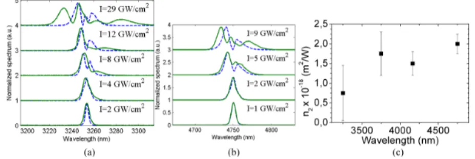
cross-section waveguide using optical pulses centered at four different wavelengths (3250 nm, 3750 nm, 4162 nm, and 4750 nm). The spectra measured at the output of the waveguide with the scanning monochromator are shown in Figs. 3(a)-3(d) for increasing powers. It can be seen that as the peak coupled intensity increased, more and more side lobes appeared, which is characteristic of SPM. In Fig. 3(e), the experimental spectral broadening calculated from the spectra [20], was found to be a sub-linear function of the coupled peak intensity, which indicated the presence of nonlinear losses [20]. Furthermore, as the coupled peak intensity increased, the spectra in Figs. 3(a)-3(d) became asymmetrical and the mean wavelength, calculated in Fig. 3(f), was slightly blue shifted with respect to that at low power. This was also observed in Si waveguides using picosecond pulses in the near-infrared where it was attributed to free-carriers generated by two-photon absorption [21,22].
Fig. 3. (a-d) Normalized transmitted spectrum as a function of the coupled peak intensity for picosecond pulses centered at wavelengths between 3.25μm and 4.75μm. (e) and (f) Spectral broadening and normalized mean wavelength shift (i.e. (λc-λ0)/λ0 where λc is the mean
wavelength of the spectrum and λ0 is the low power mean wavelength) as a function the
coupled peak intensity.
The asymmetry in the transmitted pulses is actually more pronounced than one would expect for only multi photon effects and the derived mean wavelength shift seems to increase with the wavelength. Although, at a fixed light intensity, one would expect that fewer free carriers are generated as the wavelength increases, the free carrier dispersion coefficient, kc,
scales as λ2 [12], therefore leading to a stronger effect at longer wavelengths and thus
In order to obtain the multi-photon absorption coefficients of Si0.6Ge0.4, the average output
power was measured as a function of the coupled peak intensity and the results are shown in Fig. 4(a). The nonlinear, normalized, transmission (TNL) through the waveguide as a function
of coupled peak intensity is also shown in Fig. 4(b). It is estimated from TNL = Pout/[Pin
*exp(-αL)], where Pout and Pin are the output and input coupled powers, α is the propagation loss
coefficient and L is the waveguide length. From Fig. 4(a) we observed that the output power increased almost linearly with the input power at low intensities. The slope is in agreement with the wavelength dependence of the linear losses measured on Fig. 2, i.e. a decrease of the linear loss for increasing wavelengths. This behavior confirms that the contribution of the nonlinear absorption remains negligible for coupled peak intensities below about 3 GW/cm2,
as was used earlier for the cut-back measurements. As the coupled peak intensity increased further, the output power from the waveguide saturated and eventually decreased for the two longest wavelengths. Accordingly, the nonlinear transmission in Fig. 4(b) shows a rapid drop as the input pulse intensity increased. This behavior is a clear indication of the presence of nonlinear losses in the waveguide. This trend is similar to the one observed in the case of optical limiting in the near-infrared region [21,23], which is caused by two-photon absorption and the subsequent absorption by the generated free-carriers. As the wavelength range used in our experiment is beyond the two-photon absorption threshold of Si0.6Ge0.4 (i.e. λth≈2.45 μm
[16]) the nonlinear transmission observed in Fig. 4 is necessarily due to higher order multi-photon absorption, such as three- and four-multi-photon absorption, as well as the resulting free-carrier absorption [12].
Fig. 4. (a) Output power from the Si/SiGe waveguide as a function of the coupled peak intensity for all the wavelengths used in the experiments. (b) Normalized transmission as a function of the coupled peak intensity.
5. Discussion
We used the nonlinear Schrödinger equation (NLSE) to model the nonlinear response of the SiGe/Si waveguides. The standard NLSE was modified in order to include higher order multi-photon absorption as well as free-carrier effects [20]. For example, if we were considering both three- and four-photon absorption, the NLSE would be given by
( )
2
2 4 6
0 2 3 4
2 2 2 3
3eff 5eff 7eff
i i 1 i 2 2 A 2A 2A 2 PA PA c k n A A A A A A A A A N A z t α α α σ β μ ∂ + ∂ + = − − − − ∂ ∂ (1)
where A is the slowly varying envelope of the pulse electric field amplitude; β2 is the group
velocity dispersion; α is the linear loss parameter; k0 is the wavenumber; n2 is the nonlinear
refractive index; α3PA and α4PA are the three and four-photon absorption coefficients; A3eff,
A5eff and A7eff are the effective mode areas related to the nonlinear phenomena of different
orders [24]; σ is the free-carrier absorption parameter; and μ = 2kck0/σ with kc the free-carrier
dispersion parameter. The rate equation of the free-carrier density, Nc, in the case described
3 4 2 2 3 4 5 7 A A 3 4 c PA PA c eff eff c N N t A A α α ω ω τ ∂ = − − ∂ (2)
where ħ is the reduced Plank constant; ω is the central angular frequency of the input pulse; and τc is the free-carrier lifetime. Since the range of values for τc reported for integrated
waveguides is much longer than our pulse duration and much shorter than the time period between two subsequent pulses, we can neglect the last term on the right hand side of Eq. (2) [20]. As a starting point, we used the values of Si for the free-carrier absorption and dispersion parameters and we applied the scaling rules for the wavelength used in [12]. Thus we defined σ(λ) = 1.45x10⁻²¹ x (λ/1.55)2 m2 and k
c(λ) = 1.35x10⁻²⁷ x (λ/1.55)2 m3, where λ is
the wavelength (in μm).
The NLSE in Eq. (1) was solved numerically using the Split-Step Fourier Method. We began by estimating the multi-photon absorption coefficients from the nonlinear transmission measurements that were shown in Fig. 4(b). In this step the Kerr effect and the free-carrier dispersion were neglected because they only affect the pulse phase and do not contribute to the nonlinear losses under our experimental conditions. The multi-photon absorption phenomenon considered at each of the experimental wavelengths was chosen following the model developed by Wherrett [25], i.e. by considering the ratio between the indirect bandgap energy of Si0.6Ge0.4 (Eg = 1.01 eV) and the photon energy. Additionally, the different trends of
the nonlinear transmission that are observed in Fig. 4(b) confirm that the regimes associated with the four investigated wavelengths are dominated by different multi-photon absorption orders. Therefore, up to a wavelength of 3750 nm, only three-photon absorption (α3PA) is
considered. At a wavelength of 4162 nm both three- and four-photon absorption are taken into account while at 4750 nm only four-photon absorption (α4PA) is considered. In Figs. 5(a)-5(d)
the transmission predicted by the model (continuous line) is compared to the experimental results (circles) and good agreement between the theory and the experiment is obtained. The multi-photon absorption coefficients that were estimated from our model are summarized and compared to the ones of Si and Ge in Fig. 5(e). The uncertainty in the values is mainly due to the uncertainty in the power that was coupled to the waveguides. We note that the estimated multi-photon absorption coefficients of SiGe are on the same order of magnitude as those for crystalline Si when the same order of multi-photon process is considered [12,26].
Fig. 5. (a-d) Nonlinear transmission deduced from the measurements as a function of the coupled peak intensity (circles) at different wavelengths. The nonlinear transmission predicted by solving the NLSE (continuous line) is shown along with the experimental results. (e) Comparison of three- and four-photon absorption coefficients of our SiGe waveguides (estimated in this work), along with that of Si [12], and Ge [27].
After obtaining the multi-photon absorption coefficients, we used the NLSE to estimate the nonlinear refractive index, n2, of our SiGe/Si waveguides in the mid-IR. The best fits with
the experimental data are obtained for numerical calculations with an n2 of 0.75x10⁻¹⁸ m2/W
at 3.25 μm and of 2x10⁻¹⁸ m2/W at 4.75 μm (see Figs. 6(a) and 6(b)). These values of n 2 are
similar to that of crystalline Si in the same wavelength range (i.e. n2≈2.7-5.8 x 10⁻¹⁸ m2/W)
[12,26]. A similar analysis was carried out at all wavelengths used in these experiments and the value of the nonlinear refractive index found was 1.75x10⁻¹⁸ m2/W at 3.75 μm and
1.5x10⁻¹⁸ m2/W at 4.162 μm. The estimated value of n
2 as a function of wavelength is
reported in Fig. 6(c). To first order, it is roughly constant over the wavelength range of the experiment, which is consistent with the negligible dispersion of the susceptibility of Si0.6Ge0.4 in the mid-IR [16]. From a direct comparison of the spectra shown on Figs.
3(a)-3(d), one might have expected a clear increase in n2 with wavelength because the number of
peaks at the same coupled peak intensity increases. This apparent increase ends up being moderated by the decrease in the propagation loss for longer wavelengths (Fig. 2), and the impact of the different multi-photon absorption and effective areas, which are all taken into account in the simulations.
Fig. 6. Experimental (continuous line) and numerical (dashed line) transmission spectrum due to SPM as a function of the coupled peak intensity for a pulse centered at a wavelength of 3250nm, (a), and 4750nm, (b). (c) Nonlinear refractive index as a function of wavelength.
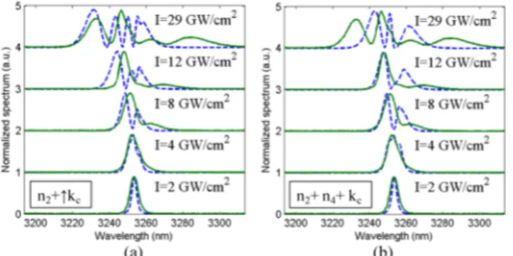
In Figs. 6(a) and 6(b), a clear deviation between the experiments and simulations is seen beyond intensities greater than 5GW/cm2, with the simulated spectral broadening underestimating the experimental one. Considering the results obtained at 3250 nm, for instance, we first investigated if this discrepancy could be due to an incorrect value for the carrier dispersion. The results shown in Fig. 7(a) were obtained by increasing the free-carrier dispersion parameter by a factor 3, i.e. up to kc = 1.78x10⁻²⁶ m3. Due to the blue shift
induced by the free-carrier dispersion, the blue part of the spectrum seems to be in slightly better agreement with the experimental results. However, the red side does not agree well with the experiment. This observation is corroborated by calculating the shift in the average wavelength of the spectrum [20], shown in Fig. 8(a). The blue shift generated by high free-carrier dispersion is too strong compared to that derived from the experimentally measured spectra (circles). Therefore, we conclude that free-carrier dispersion alone cannot explain the experimentally observed features.
Fig. 7. Experimental (continuous line) and numerical (dashed line) transmission spectrum due to SPM as a function of the coupled peak intensity. For both scenarios n2 = 0.75x10⁻¹⁸ m2/W,
then on the left kc = 1.78x10⁻²⁶ m3 while on the right n4 = 5x10⁻³³m4/W2 and kc = 5.95x10⁻²⁷m3
A second possible reason for discrepancy with our experimental results could be the presence of higher order nonlinear refractive phenomena. The polarization, P(t), induced by an intense electric field, E(t), in a centro-symmetric nonlinear medium is
(1) (3) 3 (5) 5 (7) 7
0
( ) ( ) ( ) ( ) ( )
P t =ε χ E t +χ E t +χ E t +χ E t + (3)
where the χ(n) terms correspond to the n-th order susceptibility. For instance, the two-photon
absorption and the quadratic intensity dependent refractive index (Kerr nonlinearity) are related to the imaginary and the real part of χ(3) respectively [20]. In our experimental
conditions, three- and four-photon absorption are present. These nonlinear losses arise from the imaginary parts of the χ(5) and χ(7) susceptibilities. Therefore, as for χ(3), the real part of
these higher order susceptibilities might have an impact at high field intensities in this wavelength range. These nonlinear phenomena would induce a change in the refractive index given by
2 3
2 4 6
n n I n I n I
Δ = + + (4)
where n4 and n6 are associated with the real parts of χ(5) and χ(7), respectively. Therefore, Eq.
(1) is modified to take into account the effect of the real parts of χ(5) and χ(7) and we obtain in
the general case:
( ) 6 2 4 2 4 6 6 3 2 4 4 2 2 0 2 3 2 3 3 5 7 5 7 i i 1 i 2 2 2 2 2 PA PA c
eff eff eff eff eff
n A n A n A A A A k A A A A A N A z t A A A A A α α α σ β μ ∂ ∂ + + = + + − − − − ∂ ∂ (5)
where the effects of the real parts of χ(5) and χ(7) are given by n
4|A|4 and n6|A|6 respectively. At
3250 nm, only three-photon absorption is considered and thus the terms relative to χ(7) (i.e. n 6
and α4PA) are both dropped in Eqs. (2) and (5). We simulated the pulse propagation through
the Si0.6Ge0.4 waveguide at wavelength 3250 nm and adjusted the n4 parameter to improve the
agreement between theory and experiment. We kept the same value of n2 as before,
considering that this term dominates the pulse spectral broadening at low intensities. The results shown in Fig. 7(a) were obtained using n4 = 5x10⁻³³ m4/W2 along with the same value
of kc = 5.95x10⁻²⁷ m3 as in the initial simulation (Fig. 6(a)). From the results shown in Fig.
7(b) we obtained a better agreement between the experimental and numerical results than with standard theory shown in Fig. 6(a). Thus, the evolution of the spectral broadening is better reproduced by the model developed in Eq. (5) rather than the model of Eq. (1). This can also be seen by calculating the mean wavelength shift as shown in Fig. 8(a).
Fig. 8. (a) and (b) Mean wavelength shift and spectral broadening as a function of the coupled peak pulse intensity for the three simulation scenarios. For all the curves n2 = 0.75x10⁻¹⁸ m2/W.
For the black curve kc = 5.95x10⁻²⁷ m3 as in Fig. 6(a), for the red kc = 1.78x10⁻²⁶ m3 as in Fig.
7(a), while for the green n4 = 5x10⁻³³m4/W2 and kc = 5.95x10⁻²⁷m3 as in Fig. 7(b).
We see that for low peak intensities, up to about 5 GW/cm2, the numerical results do not
differ significantly depending on whether n4 is included or not. On the other hand, at high
peak intensities the wavelength shift is reduced when both n2 and n4 are considered due to the
quadratic dependence of the induced refractive index change with pulse intensity arising from n4. The RMS spectral broadening calculated from the different simulation scenarios are
compared to the experimental ones in Fig. 8(b) and demonstrate that including both n2 and n4
gives the better agreement with the experimental results of both Figs. 8(a) and 8(b).
Similar results were found also for the pulse centered at 4750 nm. In this case, since the four-photon absorption process is present, from Eq. (5), both n4 and n6 were considered but
α3PA is neglected in both Eqs. (2) and (5) as three-photon absorption is considered to be
negligible at this wavelength. From the results shown in Fig. 9 we found that, once again, the evolution of the spectral broadening is better described when the real parts of χ(5) and χ(7) are
included.
Fig. 9. (a) Experimental (continuous line) and numerical (dashed line) transmission spectrum as a function of the coupled peak intensity calculated considering the real parts of χ(5) and χ(7).
The values used are n2 = 2x10⁻¹⁸ m2/W, n4 = 1x10⁻³⁴ m4/W2, n6 = 5x10−46 m6/W3 and kc =
1.27x10⁻²⁶ m3. (b) and (c) Mean wavelength shift and spectral broadening as a function of the
coupled peak pulse intensity. For both curves n2 = 2x10⁻¹⁸ m2/W and kc = 1.27x10⁻²⁶ m3. For
the green curve n4 = 1x10⁻³⁴ m4/W2 and n6 = 5x10−46 m6/W3.
6. Conclusions
We report measurements of the nonlinear optical response of low-loss Si0.6Ge0.4/Si
waveguides in the mid-IR between 3250 nm and 4750 nm. In this wavelength range, nonlinear losses due to multi-photon absorption and the associated generation of free-carriers are observed at high peak intensities. The three- and four-photon absorption coefficients of Si0.6Ge0.4 were estimated and were found to be comparable to those of crystalline Si and Ge.
Furthermore, the nonlinear refractive index, n2, was estimated from spectral broadening
measurements. We found that theory that accounts for free-carrier effects, multi-photon absorption and the Kerr effect was able to correctly predict the experimental results for peak intensities up to at least 5 GW/cm2, while by including higher-order nonlinear refractive
effects arising from the real parts of χ(5) and χ(7) we obtained a better agreement with
experiments for higher pulse intensities. This suggests that the effect of these phenomena is not negligible in the wavelength range considered and at the pulse intensity levels used in the experiments. This could be caused by the fact that in the mid-IR we are close to the resonance frequencies of these higher order susceptibilities, which is also consistent with our observation of three- and four-photon absorption. These results represent the first experimental characterization of the nonlinear optical response of Si0.6Ge0.4/Si waveguides in
the mid-IR and they will be useful for the design of future photonic devices based on this material platform and go a long way to understanding the optical nonlinear response of this material in the mid-IR wavelength range.
Acknowledgments
This research was supported by the People Program (Marie Curie Actions) of the European Union's Seventh Framework Program FP7/2007-2013 under REA grant agreements n°PCI-GA-2013-631543 and n° PCIG10-GA-2011-304005, the French National Research Agency (ANR project MOREMIR) and was conducted within the context of the International Associated Laboratory “ALPhFA: Associated Laboratory for Photonics between France and Australia”. This research was in part supported by the Australian Research Council Centre of Excellence for Ultrahigh bandwidth Devices for Optical Systems (project number CE110001018).