www.afm-journal.de
Interactions between Primary Neurons and Graphene Films
with Different Structure and Electrical Conductivity
Andrea Capasso,* João Rodrigues, Matteo Moschetta, Francesco Buonocore,
Giuliana Faggio,* Giacomo Messina, Min Jung Kim, Junyoung Kwon, Ernesto Placidi,
Fabio Benfenati, Mattia Bramini, Gwan-Hyoung Lee, and Nicola Lisi
Graphene-based materials represent a useful tool for the realization of novel
neural interfaces. Several studies have demonstrated the biocompatibility of
graphene-based supports, but the biological interactions between graphene and
neurons still pose open questions. In this work, the influence of graphene films
with different characteristics on the growth and maturation of primary cortical
neurons is investigated. Graphene films are grown by chemical vapor deposition
progressively lowering the temperature range from 1070 to 650
°C to change the
lattice structure and corresponding electrical conductivity. Two graphene-based
films with different electrical properties are selected and used as substrate for
growing primary cortical neurons: i) highly crystalline and conductive (grown
at 1070
°C) and ii) highly disordered and 140-times less conductive (grown at
790 °C). Electron and fluorescence microscopy imaging reveal an excellent
neuronal viability and the development of a mature, structured, and excitable
network onto both substrates, regardless of their microstructure and electrical
conductivity. The results underline that high electrical conductivity by itself is
not fundamental for graphene-based neuronal interfaces, while other physico–
chemical characteristics, including the atomic structure, should be also
consid-ered in the design of functional, bio-friendly templates. This finding widens the
spectrum of carbon-based materials suitable for neuroscience applications.
DOI: 10.1002/adfm.202005300
1. Introduction
In the last years, the combined advance-ments in biomaterial science and neu-rotechnology led to a big leap in neural tissue engineering research. In this scenario, innovative materials can be designed to engineer advanced biological interfaces that can adapt to the central nervous system and interact with it.[1,2] To
build an original platform for potential applications in neurobiology, it is pivotal to ascertain if and how a new material inter-feres with neuronal activity and/or can be manipulated to regulate it. Graphene, a representative 2D material characterized by sp2-hybridized carbon atoms in a
honey-comb arrangement,[3–5] yields gapless
semi-metal characteristics[6,7] with high carrier
mobility[4,6,8] and thermal conductivity.[9]
The distinctive properties of graphene have motivated its experimental applica-tions in a variety of fields, including elec-tronics, energy storage, composites[10–22]
Dr. A. Capasso, J. Rodrigues
International Iberian Nanotechnology Laboratory (INL) Braga 4715-330, Portugal
E-mail: [email protected]
Dr. M. Moschetta, Prof. F. Benfenati, Dr. M. Bramini Center for Synaptic Neuroscience and Technology Istituto Italiano di Tecnologia
IRCCS Ospedale Policlinico San Martino Genova 16132, Italy
Dr. F. Buonocore, Dr. N. Lisi
Agenzia nazionale per le nuove tecnologie
l’energia e lo sviluppo economico sostenibile (ENEA) Casaccia Research Centre
Roma 00196, Italy
The ORCID identification number(s) for the author(s) of this article can be found under https://doi.org/10.1002/adfm.202005300.
Dr. G. Faggio, Prof. G. Messina
Dipartimento di Ingegneria dell’Informazione delle Infrastrutture e dell’Energia Sostenibile (DIIES) Università “Mediterranea” di Reggio Calabria Reggio Calabria 89122, Italy
E-mail: [email protected] M. J. Kim, Dr. J. Kwon
Department of Materials Science and Engineering Yonsei University
Seoul 03722, Korea Dr. E. Placidi Dipartimento di Fisica Università di Roma La Sapienza Roma 00185, Italy
Dr. E. Placidi Dipartimento di Fisica Università di Roma Tor Vergata Roma 00133, Italy
Dr. M. Bramini
Department of Applied Physics University of Granada Granada 18071, Spain Prof. G.-H. Lee
Department of Materials Science and Engineering Seoul National University
Seoul 08826, Korea © 2020 The Authors. Published by Wiley-VCH GmbH. This is an open
access article under the terms of the Creative Commons Attribution License, which permits use, distribution and reproduction in any medium, provided the original work is properly cited.
The copyright line for this article was changed on 15 September 2020 after original online publication.
and biomedicine.[2,23–27] Graphene-based materials can be
engi-neered into advanced biological interfaces that can adapt to the central nervous system and interact with neurons, thanks to a host of tunable properties (e.g., mechanical, electrical, chemical, and frictional). To build an innovative platform for potential treatments of neurodegenerative diseases, it is pivotal to exclude any unwanted biological effects and ascertain if and how gra-phene-based materials can affect neuronal activity and/or be manipulated to regulate it. Recently, graphene-based materials, such as graphene oxide and functionalized graphene, have been used as 2D/3D templates for in vitro and in vivo neuroscientific applications, enabling stimulation of neural growth and regen-eration, as well as modulating neuronal firing properties.[28–30]
Despite a few studies in primary neurons and astrocytes,[31–35]
the physio-chemical nature of the interactions between cultured cells and carbon-based surfaces is not fully understood. It has been shown that chemically modified graphene featuring high wettability fosters biocompatibility and increases the adhesion of biomolecules,[28,30,36,37] displaying its potential incorporation
in biological systems. Graphene-based materials were reported to affect electron transfer of biomolecules[38,39] and couple
elec-trically with neural stem cells.[40] Moreover, graphene appeared
to influence neuronal excitability by restricting the mobility of K+ ions near the graphene surface deposited onto electrically
insulating substrates.[29] Nevertheless, there is a need to further
investigate the capability of graphene-based supports to promote the neuronal activity from a morphological and physiological point of view, taking into consideration the distinct electrical, chemical, and structural properties of graphene.
Nowadays, the production of graphene by chemical vapor deposition (CVD) affords high standards in terms of materials quality, scale and cost, which suit the requirements of different applications and indicate the way toward a sustainable mass production.[41–43] CVD provides a favorable flexibility in the
design of the graphene films’ properties, which can be aptly tuned by adjusting the process parameters. Polycrystalline gra-phene films with a wide range of grain size and electrical con-ductivity can be produced. Single-crystal graphene with a large grain size and monolayer amorphous carbon with infinitesimal grain size sit at the respective ends of the range, being electri-cally conductive and insulating, respectively. In the latter case, a form of “insulating amorphous graphene” (i.e., a freestanding, continuous and stable monolayer of sp2-bonded carbon atoms
with amorphous structure) has been recently reported.[44] In
between the two extremes, the use of ethanol as carbon pre-cursor in CVD offers a suitable control on the grain size and electrical conductivity.[45–47]
Here, we studied the interaction of primary neurons with gra-phene-films with different structure and electrical conductivity grown by ethanol-based CVD at various temperatures (span-ning from 650 to 1070 °C). While the temperatures >1000 °C led to the formation of polycrystalline graphene with large grain size[48–50] and sheet resistance values below 1 kΩ □−1,[51,52]
lowering the growth temperature reduced the grain size, with a corresponding increase of grain boundaries, structural disorder and electrical resistance (up to 70 kΩ □−1). Neurons grown on both high and low conductivity graphene films supported on poly(ethylene terephthalate) (PET) substrates formed a highly structured and mature network, with no clear alteration of their physiological activity. Intriguingly, the neuronal network archi-tecture tended to improve onto low-conductivity graphene as compared to pristine graphene, suggesting that an insulating astrocyte-like environment (induced by nanocrystalline or sp3
carbon regions) might decrease the degree of neuronal cell clumping and favor neuron spreading, without affecting the cells’ physiological activity. The observation that electrical con-ductivity by itself is not the crucial property to foster the activity of neuronal networks highlights a key point to be considered for the design of future graphene-based implants.
2. Results
2.1. Synthesis and Characterization of Graphene Films
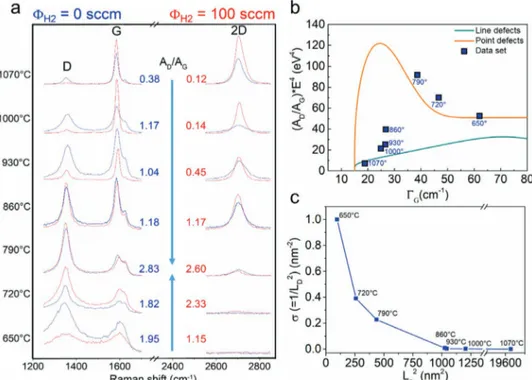
In our CVD experiments with ethanol as precursor, we varied the growth temperature from 650 to 1070 °C, using two different hydrogen flows (0 and 100 sccm). Figure 1 shows the Raman spectra of all samples grown at the different temperatures.
Both the temperature and hydrogen flow clearly affected the structural properties of the films (Figure 1a). In the high-temperature range of 930–1070 °C, the Raman spectra show the distinct features of graphene.[46,54] The integrated intensity
ratio of D and G peaks (AD/AG) (indicated along the graphs
in Figure 1a) decreased with the temperature, indicating improved crystallinity and reduced disorder. When adding hydrogen as co-carrier gas, less defective graphene films were grown. This is in line with previous observations, which indi-cated that hydrogen co-carrier gas could slow down the growth process kinetics and balance the carbon etching action deriving from the oxygen-containing species, such as water vapor, released by the ethanol pyrolysis during CVD.[45,55,56] When
no hydrogen is added to the gas mixture, this etching action is generally excessive, reducing the crystalline quality of gra-phene. At the intermediate temperatures (790–860 °C), Raman spectra are similar regardless of the hydrogen flow. Although both the 790 and 860 °C spectra show an intense and narrow D peak, only the 860 °C spectrum retains marked G and 2D bands (evidence of a crystalline sp2 carbon structure with high
defect density). The 790 °C spectrum shows only a residual 2D band and, as a result, has the highest AD/AG ratio (as reported
in Figure 1b).[47] In the lower temperature range (650–720 °C),
the Raman spectra show that the graphene films are highly
disordered.[57,58] In the intermediate and low temperature
range, the drawbacks from oxidative etching become less evi-dent and thus the balancing effect (i.e., reduction) from the H2
Prof. G.-H. Lee
Research Institute of Advanced Materials (RIAM) Seoul National University
Seoul 08826, Korea Prof. G.-H. Lee
Institute of Engineering Research Seoul National University Seoul 08826, Korea Prof. G.-H. Lee
Institute of Applied Physics Seoul National University Seoul 08826, Korea
co-carrier gas is not observed. This is supported by the AG/AD
ratios in Figure 1a, which are markedly different in the high temperature range but become similar at low/intermediate range, meaning that the balancing effect on H2 is masked by
the general defectiveness increase due to the lower tempera-ture. Hydrogen might actually slow down the dehydrogenation of the precursor (and the accretion of the forming crystal) espe-cially at low temperatures.[56] Therefore, the graphene-films
grown in this work are categorized into less defective graphene for T > 790 °C and more defective graphene for T < 790 °C, based on the non-monotonic curve of the AD/AG ratio versus
the temperature and sudden increase of FWHM (Γ) of D, G
and D’ peaks (Figure S1, Supporting Information). To quanti-tatively analyze the Raman spectra, we used a model proposed by Cançado.[53] Figure 1b shows the amorphization
trajecto-ries (Raman diagram) for graphene films, revealing point-like and line-like defects. The orange and green curves delimit the region where point and line defects can coexist. The data points of the graphene films grown at T > 860 °C are close to the curve of line defects (green line); meanwhile, at T < 860 °C, the data points are on the curve of point defects (orange line). As shown in Figure 1c of the point defect density (σ = 1/LD2)
versus grain size (La2) (see Supporting Information for a more
detailed description), graphene grown at high temperature showed larger grain size (140 nm at 1070 °C) with very low point defect density; meanwhile, at low temperature, graphene has small grain size (10 nm at 650 °C) with very high point defect density.
We analyzed the electrical and optical properties of the gra-phene films grown at different temperatures. In previous work,
we reported that the sheet resistance (Rs) of the graphene
films grown by the same process increases with decreasing growth temperature (from 0.5 kΩ □−1 at 1070 °C to 2.4 kΩ □−1
at 930 °C), maintaining high optical transmittance of ≈90% ± 1% at 550 nm, regardless of the temperature (Figure S2, Sup-porting Information).[46] Here, we further investigated the
graphene grown at lower temperatures, down to 650 °C. We
fabricated graphene field-effect transistors (FETs) to measure the sheet resistance and field-effect mobility (μFE) using
the transfer length method (TLM—as described in the Experi-mental Section). Figure 2a shows the representative graphene FETs fabricated on a Si/SiO2 substrate (heavily doped Si with
thermally grown SiO2 of 285 nm). The linear output curves of
the 790 °C graphene device indicates that the contact resistance is negligibly small (Figure 2b). The transfer curves of the same device with various channel lengths (from 5 to 40 µm with a 5 µm step, Figure 2c) showed that graphene is highly p-doped, probably due to the substrate and adsorbed molecules (upon air exposure). The field-effect mobility (μFE) was extracted from the
slope of the transfer curves using the Equation (1) below:
µ = d d FE i ds ds bg L WC V I V (1)
where L, W, and Ci are channel length, width, and
capaci-tance, respectively. The sheet resistance (Rs) of each sample
Figure 1. a) Raman spectra of graphene grown for 30 min at 650–1070 °C with or without hydrogen flow (0 and 100 sccm of H2 as indicated by blue and
red lines, respectively). The AD/AG ratios (blue values for no H2 flow and red values for H2 flow of 100 sccm) are indicated along the arrows that show
an increase of the values (maximum at 790 °C). b) Plot of the data set calculated as the AD/AG ratio multiplied by the fourth power of the excitation
laser energy (2.41 eV) versus the full-width-at-half-maximum (FWHM) of the G peak (ΓG). The plot illustrates the “amorphization trajectory” proposed
by Cançado et al. (referring to Equations (1) and (4).[53] c) Plot of the defect density (σ) versus crystallite area (L
a2). The data sets in (b) and (c) refer
was extracted from the slope of the total resistance (Rtot)
versus channel length (Lch) plot (Figure S3, Supporting
Infor-mation). As shown in Figure 2d, the sheet resistance of the graphene significantly increased from 18 to 375 kΩ □−1 with decreasing growth temperature from 860 to 650 °C. The field-effect mobility showed the opposite trend, varying from 26 to 1.5 cm2 Vs−1. The changes in R
s and μp in Figure 2d are in good
agreement with the trend of defect density (σ) obtained by the
Raman analysis (Figure 1c). The electrical measurement results clearly show that sheet resistance and defect density have a linear relationship in logarithmic scale (Figure S4, Supporting Information). This strongly suggests that we can precisely modulate the sheet resistance of the grown graphene with the growth temperature by controlling its morphology and struc-ture, in terms of grain size, defect type, and defect density.
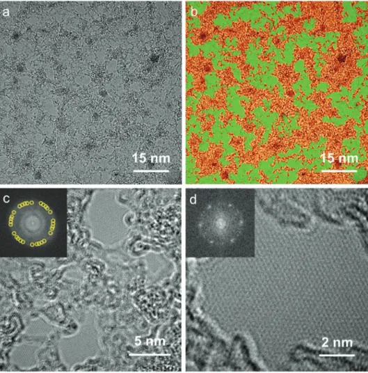
The film grown at 790 °C showed graphene-like features in Raman spectra, but had very high sheet resistances (70 kΩ □−1). To account for this different electrical behavior, we further analyzed its microstructure by transmission electron microscopy (TEM). The film was transferred onto holey-carbon grids (Figure S5a, Sup-porting Information). The film edge in Figure S5b, SupSup-porting Information reveals its monolayer thickness. Figure 3a highlights its lattice structure. To help the visualization the crystalline grains, crystalline, and disordered regions are identified with different colors in Figure 3b. The film is composed of two intermixed car-bonaceous phases: crystalline nanograins with size in the order of 5–20 nm (light green areas) are surrounded by a disordered carbon structure (orange areas).
Figure 3c shows a close-up TEM image of the film. The five sets of sixfold spots in the FFT (inset of Figure 3c) indicate the presence of misoriented crystalline graphene grains. Figure 3d
is a higher magnification TEM image of a single grain. The inset shows the sixfold spots in the FFT pattern, typical of a gra-phene single crystal. The sp2 grain is embedded in a highly
dis-ordered region. The 860 °C film was also analyzed by TEM for comparison. This film showed a structure similar to the 790 °C film, but the crystalline grain size was found to be on average larger, as reported in the representative images in Figure S6, Supporting Information and expected for a higher CVD tem-perature. Our structural and electrical analyses show that the microstructure of graphene, as well as the sheet resistance, can be finely controlled by temperature in ethanol-CVD processes. We further investigated the 790 °C sample by X-ray photoelec-tron spectroscopy (XPS) to analyze the elemental composition
in comparison to the standard graphene sample (1070 °C).
The C1s peak of the 1070 °C graphene consists entirely of sp2
(Figure S7a, Supporting Information); meanwhile, the peak of
the 790 °C graphene has two main components of sp2 (60%)
and sp3 (40%) carbons (Figure S6b, Supporting Information). Electron energy loss spectroscopy was used to ascertain the potential formation of CH bonds, (Figure S8, Supporting Information). The spectrum of the 790 °C graphene showed a more intense peak for stretching mode of CH vibration than 1070 °C graphene. Hydrogenated carbon bonds are likely to be formed in the disordered regions (sp3) of the 790 °C film.
2.2. Toward the Biological Interface: Sample Selection and Further Characterization
To characterize the graphene templates for a biological per-spective, we used two graphene samples with markedly
Figure 2. a) Optical image of the graphene FETs with TLM geometry. The channel lengths range from 5 to 40 µm with a step of 5 µm. b) Output curves (Ids–Vds) at various back gate voltages (Vbg) of the graphene device grown at 790 °C with 0 sccm H2 flow. c) Transfer curves (Ids–Vbg) of the same device
different electrical conductivities: highly crystalline graphene grown at 1070 °C (G1070) with Rs = 500 Ω □−1 and highly
dis-ordered graphene grown at 790 °C (G790) with Rs = 70 kΩ □−1.
We measured the morphology of the G1070 and G790 by
atomic force microscopy (AFM) after transfer onto the Si/SiO2
substrates as shown in Figure 4a,b, respectively. The height profiles of the torn edges confirm that both have similar thickness.[47]
Figure 3. TEM images of the graphene grown at 790 °C. TEM images of the graphene film composed of two intermixed carbonaceous phases: a) as-obtained and b) false-colored images. Higher magnification images of c) polycrystalline region and d) single grain region. Note that the scale bars are different in all images.
In neuronal interfaces, increasing levels of surface roughness have been connected to a facilitated neuronal adhesion.[59,60]
Therefore, the surface roughness of the G1070 and G790 was measured from the topographic AFM data (Figure S9, Sup-porting Information). On average, the two samples presented similar surface heights (<2 nm) and roughness (<1 nm), within the expected ranges for transferred monolayer graphene grown by CVD.[61,62]
2.3. Graphene Films with Different Crystallinity and Conductivity are Both Efficient Substrates for Neuronal Interfaces
To investigate the effect of structure and conductivity of gra-phene on neuronal properties, the G790 and G1070 films were transferred onto insulating PET substrates. First, the wetting angles of PET/G790 and PET/G1070 were measured with a water droplet. Bare PET, PET/G790, and PET/G1070 showed the
wetting angles of 84.4°, 77.1°, and 84.2° respectively, revealing a similar hydrophilicity.[63] In particular, PET/G1070 has the same
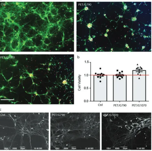
wetting angle of PET, demonstrating the “wetting transparency” expected for standard graphene.[64] Rat cortical primary neurons
were grown onto PET-supported graphene films and their via-bility and firing properties were investigated after 14 days of cul-ture. Cells were stained with Hoechst-33342 to mark all nuclei, propidium iodide (PI), and fluorescein diacetate (FDA) to dis-tinguish dead and viable cell, respectively. All treated samples were then imaged by epifluorescence microscopy (Figure 5a). The results clearly show that the viability of primary neurons was well preserved on all substrates (Figure 5b). However, net-work formation and neuronal morphology were slightly altered in cultures grown onto graphene films, where a few cell clus-ters and aggregates were observed. In particular, cultures grown on PET/G790 resembled those grown on control glass sub-strates, while neurons grown onto PET/G1070 clearly displayed a higher degree of clusterization. These differences might be
Figure 5. Neuronal viability. a) Primary rat cortical neurons were grown onto glass (Ctrl), PET/G1070 and PET/G790 for 14 days. Cell viability was
evaluated by fluorescence microscopy. Representative images of cultures stained with Hoechst-33342 for nuclear visualization (in blue), Fluorescein Diacetate (FDA, in green) for viability detection and Propidium Iodide (PI, in red) for cell death quantification are displayed (scale bars: 100 µm). b) Viability was quantitatively assessed by calculating, for each experimental group, the percentages of PI-positive cells with respect to the total number of Hoechst-positive cells. Viability values were normalized to the respective average value of the Ctrl samples, set to 1 and plotted as means ± sem with individual experimental points. No significant changes in cell viability were observed under the various experimental conditions (one-way ANOVA and Bonferroni's post-hoc test, n = 10 fields per experimental condition, from two independent neuronal preparations). c) SEM micrographs are reported and display that cell morphology was substantially unaffected in all substrates.
explained by the residual higher degree of hydrophobicity of graphene films compared to glass control. One of the biggest issues for graphene bio-templates is their intrinsic hydropho-bicity, which would impede a proper cell adhesion and network development. However, our data display that a certain level of hydrophobicity is well tolerated by primary neurons. In addi-tion, scanning electron microscopy (SEM) allowed us to explore in more detail the network morphology and the growth and arborization process (Figure 5c). Despite slight cell clumping and alteration in the cellular network on PET/G1070, the overall single-cell morphology was maintained on all templates, including PET/G790 and control samples. Both SEM and fluo-rescence microscopy imaging revealed an excellent viability and sustainable network development in cultures grown onto both PET/G790 and PET/G1070, suggesting that both substrates, in spite of their different structure and conductivity display a good neuronal affinity and biocompatibility with neurons.
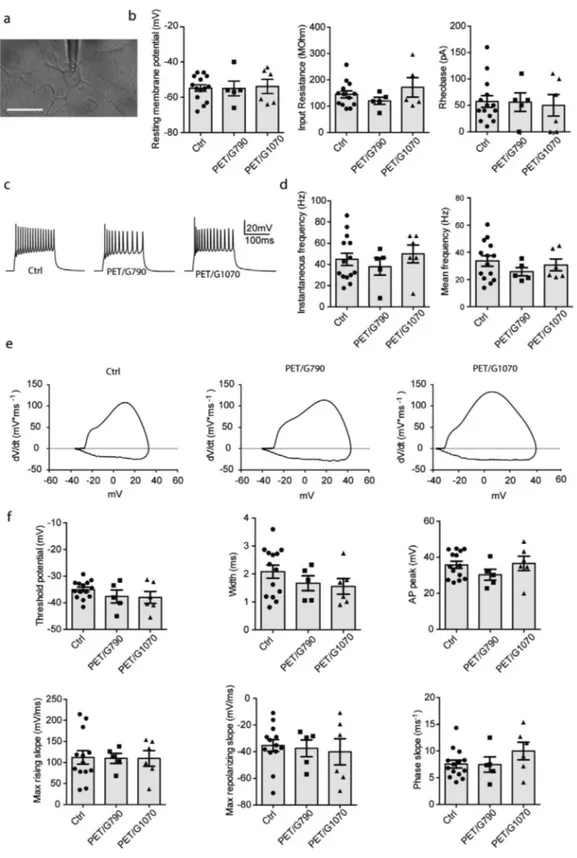
Being neurons viable on all substrates, we investigated their functional activity. To clarify the biological effects of PET-sup-ported G790 and G1070 on the neuron wellness, whole-cell cur-rent-clamp recordings were performed (Figure 6). We focused on the passive membrane properties and intrinsic excitability of single neurons by exploring if these parameters were affected by the graphene substrate microenvironment. By recording the action potentials evoked by step-like increase of injected current, the resting membrane potentials and the input resistance were evaluated as an indication of passive membrane properties.
Interestingly, cortical neurons plated onto PET/G790 and PET/ G1070 displayed no recognizable differences in their passive and active properties and in the frequency of evoked firing of action potentials, compared to the glass control sample. Neurons showed physiological values of passive membrane properties, resting membrane potential, and mean/instantaneous firing frequen-cies (Figure 6c,d), implying that the neither graphene films alter their membrane properties and intrinsic excitability. When the waveforms of single evoked action potentials were analyzed, no changes were observed in threshold voltage or AP shape parame-ters obtained from phase-plot analysis (Figure 6d,e), indicating the absence of overt effects on ion conductances.[65,66] In conclusion,
neither PET/G790 nor PET/G1070 significantly alter the physiolog-ical growth of primary neurons and the development of a mature, structured, and excitable network, indicating that both of them can serve as efficient and biocompatible neuronal interfaces.
3. Discussion
In our study, we tuned the CVD parameters to finely control the structural and electrical properties of graphene films. As a carbon precursor, ethanol is versatile and allows the forma-tion of graphene-based films with various characteristics as a function of the CVD temperature.[51,52,56] We explored an
exten-sive range of temperatures, describing the structural charac-teristics of the films and linking their electrical properties to the CVD temperatures. When lowering the CVD temperature from 1070 to 650 °C, the graphene film structure passes from crystalline, to disordered (sp2–sp3), to amorphous, with a
cor-responding decrease in electrical conductivity. To gauge the bio-logical affinity with primary neurons, we identified a monolayer film composed of graphitic nano-grains embedded in a highly
disordered carbon matrix (G790), having sheet resistance of 70 kΩ □−1 (i.e., 140 times higher than graphene). We studied the morphological and electrophysiological properties of neu-rons plated onto the low-conductivity PET/G790, and com-pared to the standard, high-conductivity, PET/G1070. As a first result, both graphene coatings resulted safe and biocompatible, allowing neuronal growth and viability similar to the standard control glass substrate. The neuronal network presented a favorably developed neurite architecture and conformation on both PET/G790 and PET/G1070, with only few sparse cell aggre-gates observed on PET/G1070. Although PET/G790 showed a wetting angle higher by 10% with respect to PET/G1070, it is unlikely that the small difference in wettability can account for the different growing pattern.[67–73] Nonetheless, no
detect-able changes in viability, morphology, and electrical properties were found in cells cultured on PET/G790 and PET/G1070, suggesting that the limited neuronal clumping observed onto PET/G1070 does not compromise cell wellness. However, the improved neuronal network architecture onto low-conductivity graphene suggests that an insulating astrocyte-like environ-ment (potentially induced by the presence of nanocrystalline or sp3 carbon regions) might favor neuron adhesion and network
development. In terms of neuronal physiology, no significant differences in passive and active firing properties and a com-parable firing frequency were detected on both PET/G1070 and PET/G790, confirming the good cell viability and suggesting that no alterations occurred in ion channel composition and maturation of intrinsic excitability. Recent publications hypoth-esized that highly conductive graphene-based materials (e.g., pristine monolayer with sheet resistance <1 kΩ □−1) could induce per se changes in neuronal excitability, altering ion channel activity.[29,74,75] It is widely believed that the electrical
conductivity should play a primary role in the interactions between nanocarbon-based substrates and cells.[29,74,76,77]
How-ever, for graphene-based films, no maximum limit of sheet resistance has been indicated as requirement to enable a proper cell adhesion and excitability. The physiological network devel-opment and cell excitability observed on G790 extend this range up to 70 kΩ □−1. G790 have different atomic structure and sp2/
sp3-hydridized carbon ratio with respect to G1070 (i.e., standard
sp2-coordinated graphene). This suggests that the acceptable
range of electrical conductivity for an efficient graphene-based interface is broader than expected, while the atomic structure and the related surface chemistry might play a role in fostering a physiological interaction with the neurons. This observation is in line with results obtained on nanodiamond monolayers (i.e., fully sp3-coordinated carbon films, with resistivity values
up to MΩ∙cm),[78] which were shown to support the growth of
neuronal cultures in terms of initial cell attachment and neu-rite outgrowth, while also fostering the neuronal network excit-ability.[79] Future studies could then focus further on the effects
and relative optimization of the structural and electrical proper-ties of nanocarbon-based coatings for biological interfaces.
4. Conclusion
Graphene-based materials are particularly suited as coatings or surface modifiers to generate advanced substrates, prostheses and biosensors for biomedical applications, particularly for neural interfaces. Despite the large amount of published
Figure 6. Passive and active properties of primary neurons grown onto different graphene substrates. a) Representative image of a single neuron
patched under current-clamp configuration (scale bar: 20 µm). b) From left to right: resting membrane potential, input resistance and rheobase. c) Representative traces of action potential firing evoked by 250 pA current injection. d) Instantaneous firing frequency (left) and mean firing frequency (right) evoked by injection of 250 pA depolarizing current. e) Representative phase-plot analysis of the action potential waveform in each experimental condition obtained by plotting the first derivative of the membrane voltage (dV/dt) versus membrane voltage (Vm). f) From left to right: threshold
potential, width and AP peak (upper row) and max rising slope, max repolarizing slop and phase slope (lower row). All data are shown as means ± sem with individual experimental points. All the analyzed parameters were not significantly different among experimental groups; one-way ANOVA/ Bonferroni’s post-hoc test (n = 5–14 cells, from two independent neuronal preparations).
papers and the proven good biocompatibility of graphene-based supports, one of the current open question is how graphene-based substrates interact with living neurons. We demonstrated that the high electrical conductivity in a graphene film is not a necessary condition for the fabrication of efficient neuronal bio-interfaces and infer that other intrinsic features of the gra-phene-based interface, such as the lattice structure and surface chemistry, might play a more fundamental role. Our results enlarge the spectrum of carbon-based materials suitable for neuroscience applications, the potential use of CVD-grown gra-phene materials for implants, especially for the nervous system.
5. Experimental Section
Growth and Transfer of Graphene-Based Films: Graphene-based films
were grown by ethanol-CVD on Cu foils (25 µm thick, 99.95% purity) at low-pressure (4 mbar) using Ar and H2 as carrier gases. A
custom-made CVD system used in this work consists of a quartz tube (length = 2 m) coaxial to the furnace, vacuum pumps (rotary vane and turbo-molecular pump), a digitally controlled gas/vapor feed system, either quartz or tantalum boat sample holders. A schematic of the system can be found elsewhere.[80] The samples can be rapidly inserted and
extracted from the hot zone, thus allowing for the rapid cooling of the samples. For the film growth, the Cu foils were inserted into the hot zone and annealed for 20 min at the growth temperature while flowing Ar/H2 (20/20 sccm). After annealing, the synthesis was performed by
bubbling ethanol in the chamber (CH3CH2OH/Ar = 0.1/20 sccm);
hydrogen was used as co-carrier gas when specified in the Results section (H2 = 0 or 100 sccm). The growth temperature ranged from
1070 °C (just below copper’s melting point) to 650 °C in 70 °C steps. After the growth time (30 min), the samples were rapidly extracted from the hot zone and let cool down to ambient temperature before leaving the controlled atmosphere environment. Before the transfer process, the carbon layer grown on the back of the Cu foil was removed by O2
plasma cleaning (O2 plasma condition: 20 sccm/100 W/3 min/100 kHz,
Femto Plasma Cleaner, Diener Electronics). For the transfer, few drops of cyclododecane/dichloromethane solution[81] (20% mass) were spin
coated on the sample, which was heated at 80 °C on a hot plate for a few seconds. The coated sample was floated in an ammonium persulphate solution (120 g L−1 in distilled water) at 4 °C for 3 h to etch the Cu foil.
After the complete Cu etching, the graphene-based films were scooped for the solution with a clean microscope slides and transferred to DI water for rinsing (a step repeated three times). At last, the graphene-based film was scooped and transferred to the target substrates. This procedure allowed maintaining the film integrity over a few square centimeters in all cases. This procedure was used to transfer all the samples onto specific substrates for characterization purposes (expect for TEM analysis, as described below) and for the neuron morphological and electrophysiological tests.
Characterization of the Films—Raman Spectroscopy: The films were
transferred onto Si/SiO2 (300 nm). A Ramanor U1000 with double
monochromator and an electrically cooled Hamamatsu R943-02 photomultiplier for photon-counting detection was used to collect the Raman spectra. The laser beam (Ar+, 514.5 nm) was focused to a diameter
of ≈1 µm, taking care of minimizing surface heating (power below 1 mW).
Characterization of the Films—FET Fabrication and Electronic/Electrical Measurements: Cyclododecane (CDD) dissolved in hexane (20% mass)
was spin coated on graphene-based films grown at 650, 720, and 860 °C. CDD/graphene based-films was heated at 80 °C on a hot plate for a few seconds poly-methyl methacrylate (PMMA) was spin coated on a based film grown at 790 °C (3000 rpm for 1 min). The graphene-based films used to fabricate FETs were synthesized under 20 sccm of Ar (0.5% CH3CH2OH diluted in Ar). The carbon layer grown on the back of
the Cu foil was removed by O2 plasma cleaning (O2 plasma condition:
20 sccm/100 W/3 min/100 kHz, Femto Science). The Cu foil was etched by ammonium persulfate (20 wt% solution) for 2 h. The CDD/graphene and PMMA/graphene sample were scooped and rinsed in DI water.
Finally, the CDD/graphene and PMMA/graphene samples were scooped with a Si/SiO2 (285 nm), and the PMMA layer was dissolved in acetone.
After the transfer process, e-beam lithography (Raith Pioneer 2) with a negative e-beam resist (HSQ) was used to pattern the both graphene-based films. After HSQ lift-off, a second e-beam lithography step was performed to pattern the electrodes. Then, metallic contacts (Cr/Pd/Au with thickness 0.5/30/40 nm) were deposited by e-beam evaporation (at 10−7 torr) and lift-off was used to complete the device fabrication.
Cr was used as adhesive layer and Au as capping layer. The electrical measurements were carried out with a Keithely 4200 semiconductor characterization system in ambient condition.
Characterization of the Films—TEM: To prepare the TEM grids, PMMA
was spin coated on the sample (3000 rpm for 1 min). The carbon layer grown on the back of the Cu foil was removed by O2 plasma cleaning (O2
plasma condition: 20 sccm/100 W/3 min/100 kHz, Femto Science). The Cu foil was etched by ammonium persulfate (20 wt% solution) for 2 h. The PMMA/graphene sample was rinsed in DI water. Finally, the PMMA/ graphene sample was scooped with a TEM grid, and the PMMA layer was dissolved in acetone. TEM characterization was performed at 80 kV to reduce the radiation damage to graphene crystals (JEOL JEM-ARM 200F).
Characterization of the Films—AFM: The films were transferred
onto Si/SiO2 (300 nm). Atomic force microscopy was performed in
tapping-mode with fast scan axis scanning at 0.5 Hz, using Sb-doped Si cantilevers with resonant frequency of ≈300 kHz (Bruker–Veeco Dimension Icon AFM).
Characterization of the Films—XPS: XPS measurements were carried
out on samples as grown on Cu foil, after a short exposure to ambient air (<5 min), with a ESCALAB MKII VG spectrometer (base vacuum of 3.0 × 10⁻⁹ mbar). The Mg kα line (1253.6 eV) was used to acquire C1s
spectra.
Characterization of the Films—High Resolution Electron Energy Loss: As-grown samples on Cu foil were measured. Loss spectra were
measured at base a pressure of 10−10 mbar. A fixed geometry was used:
the kinetic energy of the electron beam was 10 eV and was detected at
θ = 45° from the sample normal. The energy resolution, measured as the
FWMH, was ≈30 meV on the samples.
Characterization of the Films—Contact Angle Measurements: Static
contact angles were measured by the sessile drop method at ambient temperature (20 °C) with a Dataphysics OCA 20 contact angle goniometer using 5 µL drops of Milli-Q water. The average contact angles were calculated from a series of five independent measurements by the SCA20 software.
Primary Neuronal Cultures: All experiments were carried out
in accordance with the guidelines established by the European Community Council (Directive 2010/63/EU of 22 September 2010) and were approved by the Italian Ministry of Health. The primary cortical cultures were prepared from wild-type Sprague–Dawley rats (Charles River, Calco, Italy) and all efforts were made to minimize suffering and reduce the number of animals used. Briefly, rats were sacrificed by CO2
inhalation, and 18-day embryos (E18) were removed by cesarean section. Enzymatically dissociated cortical neurons were plated on poly-d-lysine-coated (0.1 mg mL−1) glass coverslips (Ctrl; Thermo-Fischer Scientific,
Waltham, MA), PET/790, and PET/1070 (10 × 10 mm2/5 × 5 mm2) at
a density of 80.000 cells mL−1.[82,83] Cultures were incubated at 37 °C,
5% CO2, 90% humidity in medium consisting of Neurobasal (Gibco/
Thermo-Fischer Scientific) supplemented to reach final concentration of 5% glutamine, 5% penicillin/streptomycin, and 10% B27 supplement (Gibco/Thermo-Fischer Scientific).
Cell Viability: Rat cortical neurons were seeded onto PET/790
and PET/1070 and onto glass coverslips as control condition for 14 days. Live cells were stained with Propidium Iodide (1 µm) for cell death quantification, dluorescein diacetate (2 µm) for cell viability, and Hoechst-33342 (1 µm) for nuclei visualization for 3 min at room temperature. Cell viability was quantified at 20× (0.5 NA) magnification using a Nikon Eclipse-80i upright epifluorescence microscope (Nikon, Tokio, Japan), with random sampling of 5 fields per sample (n = 2 samples, from 2 independent culture preparations). Image analysis was performed using the ImageJ software and the Cell Counter plugin.
SEM Analysis: For SEM cell analysis, primary cortical neurons after
14 days were fixed with 1.5% glutaraldehyde in 66 mm sodium cacodylate buffer and post-fixed in 1% OsO4. Sample dehydration was performed
by 5 min washes in 30%, 50%, 70%, 80%, 90%, 96%, and 100% EtOH solutions. In order to fully dry the samples, overnight incubation with 100% EtOH was performed. Before SEM acquisition, coverslips were sputter-coated with a 10 nm layer of 99% gold nanoparticles in an Ar-filled chamber (Cressington, Sputter Coater 208HR) and imaged using a JEOL JSM-6490LA scanning electron microscope (JEOL Ltd., Tokyo, Japan).
Patch-Clamp Recordings: Rat cortical neurons were recorded at 12–15
days. Patch pipettes, prepared from thin borosilicate glass, were pulled and fire-polished to a final resistance of 4–5 MΩ when filled with standard internal solution. All experiments were performed at room temperature (18–24 °C). Data acquisition was performed using PatchMaster program (HEKA Elektronic). Current-clamp recordings were performed at a holding potential of −70 mV, and action potential firing was induced by injecting current steps of 10 pA lasting 500 ms. Cells were maintained in extracellular standard solution (Tyrode) containing (in mm): 140 NaCl, 2 CaCl2, 1 MgCl2, 4 KCl, 10 glucose, and 10 HEPES (pH 7.3 with NaOH),
in which D-(−)-2-amino-5-phosphonopentanoic acid (D-AP5; 50 µm), 6-cyano-7 nitroquinoxaline-2,3-dione (CNQX; 10 µm), bicuculline methiodide (BIC; 30 µm), and (2S)-3-[[(1S)-1-(3,4-dichlorophenyl)ethyl] amino-2-hydroxypropyl] (phenylmethyl)phosphinic acid hydrochloride (CGP58845; 5 µm) were added to block NMDA, non-NMDA, GABAA,
and GABAB receptors, respectively. The internal solution (K-gluconate)
was composed of (in mm) 126 K gluconate, 4 NaCl, 1 MgSO4, 0.02 CaCl2,
0.1 BAPTA, 15 glucose, 5 Hepes, 3 ATP, and 0.1 GTP (pH 7.3 with KOH). All the reagents were bought by Tocris, otherwise specified in details.
Supporting Information
Supporting Information is available from the Wiley Online Library or from the author.
Acknowledgements
A. Mehilli is gratefully acknowledged for primary cell culture preparations, as well as D. Moruzzo, R. Ciancio, and I. Dallorto for technical and administrative support. The work was supported by the European Union’s Horizon 2020 Research and Innovation Programme under Grant Agreement Grant Agreement No. 785219—Graphene Flagship— Core2 and Ministero degli Affari Esteri e Cooperazione Internazionale of Italy (Farnesina—MAECI) under the Grant Agreement No. MAE0057294. G.H.L. acknowledges supports from Basic Science Research Program, the Creative Materials Discovery Program, and the International Research & Development Program through the NRF of Korea (2016M3A7B4910940, 2018M3D1A1058793, 2019K1A3A1A25000267). M.B. acknowledges the European Union’s Horizon 2020 under the Marie Skłodowska–Curie Action-COFUND Athenea3i grant agreement No. 754446. A.C. acknowledges the support of the European Union’s Horizon 2020 research and innovation program under the Marie Skłodowska– Curie grant agreement No. 713640.
Conflict of Interest
The authors declare no conflict of interest.
Keywords
2D materials, electrical conductivity, hydrophilicity, neuronal networks, poly(ethylene terephthalate)
Received: June 23, 2020 Revised: July 23, 2020 Published online:
[1] M. Bramini, G. Alberini, F. Benfenati, F. Cesca, L. Maragliano, in 2D
Materials, (Eds: C. E. Banks, D. A. C. Brownson), CRC Press, Boca
Raton, FL 2018, Ch. 4.
[2] M. Bramini, G. Alberini, E. Colombo, M. Chiacchiaretta, M. L. DiFrancesco, J. F. Maya-Vetencourt, L. Maragliano, F. Benfenati, F. Cesca, Front Syst Neurosci 2018, 12, 12.
[3] K. S. Novoselov, D. Jiang, F. Schedin, T. J. Booth, V. V. Khotkevich, S. V. Morozov, A. K. Geim, Proc. Natl. Acad. Sci. USA 2005, 102, 10451. [4] K. S. Novoselov, Science 2004, 306, 666.
[5] M. J. Allen, V. C. Tung, R. B. Kaner, Chem. Rev. 2010, 110, 132.
[6] V. E. Castro, K. S. Novoselov, V. S. Morozov, N. M. R. Peres, J. M. B. L. dos Santos, J. Nilsson, F. Guinea, A. K. Geim, A. H. C. Neto, Phys. Rev. Lett. 2007, 99, 216802.
[7] K. S. Novoselov, A. K. Geim, V. S. Morozov, D. Jiang, M. I. Katsnelson, V. I. Grigorieva, V. S. Dubonos, A. A. Firsov,
Nature 2005, 438, 197.
[8] A. K. Geim, Science 2009, 324, 1530.
[9] A. A. Balandin, S. Ghosh, W. Bao, I. Calizo, D. Teweldebrhan, F. Miao, C. N. Lau, Nano Lett. 2008, 8, 902.
[10] A. Capasso, S. Bellani, A. L. Palma, L. Najafi, A. E. Del Rio Castillo, N. Curreli, L. Cinà, V. Miseikis, C. Coletti, G. Calogero, V. Pellegrini, A. Di Carlo, F. Bonaccorso, 2D Mater. 2019, 6, 035007.
[11] A. Capasso, A. E. Del Rio Castillo, H. Sun, A. Ansaldo, V. Pellegrini, F. Bonaccorso, Solid State Commun. 2015, 224, 53.
[12] K. Kostarelos, M. Vincent, C. Hebert, J. A. Garrido, Adv. Mater. 2017,
29, 1700909.
[13] K. S. Novoselov, V. I. Fal′ko, L. Colombo, P. R. Gellert, M. G. Schwab, K. Kim, Nature 2012, 490, 192.
[14] M. Y. Han, B. Özyilmaz, Y. Zhang, P. Kim, Phys. Rev. Lett. 2007, 98, 206805.
[15] K. S. Kim, Y. Zhao, H. Jang, S. Y. Lee, J. M. Kim, K. S. Kim, J.-H. Ahn, P. Kim, J.-Y. Choi, B. H. Hong, Nature 2009, 457, 706.
[16] S. Myung, A. Solanki, C. Kim, J. Park, K. S. Kim, K.-B. Lee, Adv.
Mater. 2011, 23, 2221.
[17] S. Stankovich, D. A. Dikin, G. H. B. Dommett, K. M. Kohlhaas, E. J. Zimney, E. A. Stach, R. D. Piner, S. T. Nguyen, R. S. Ruoff,
Nature 2006, 442, 282.
[18] Y. Wang, Z. Li, J. Wang, J. Li, Y. Lin, Trends Biotechnol. 2011, 29, 205. [19] S. Watcharotone, D. A. Dikin, S. Stankovich, R. Piner, I. Jung,
G. H. B. Dommett, G. Evmenenko, S.-E. Wu, S.-F. Chen, C.-P. Liu, S. T. Nguyen, R. S. Ruoff, Nano Lett. 2007, 7, 1888.
[20] C. Wu, Y. Zhou, X. Miao, L. Ling, Analyst 2011, 136, 2106.
[21] M. I. Ortiz-Torres, M. Fernández-Niño, J. C. Cruz, A. Capasso, F. Matteocci, E. J. Patiño, Y. Hernández, A. F. González Barrios, Sci.
Rep. 2020, 10, 3376.
[22] H. Lee, M. J. Kim, J. H. Kim, J.-Y. Lee, E. Ji, A. Capasso, H.-J. Choi, W. Shim, G.-H. Lee, Mater. Res. Express 2020, 7, 045603.
[23] C. Saraiva, C. Praça, R. Ferreira, T. Santos, L. Ferreira, L. Bernardino,
J. Controlled Release 2016, 235, 34.
[24] K. Yang, S. Zhang, G. Zhang, X. Sun, S.-T. Lee, Z. Liu, Nano Lett.
2010, 10, 3318.
[25] S. R. Shin, Y.-C. Li, H. L. Jang, P. Khoshakhlagh, M. Akbari, A. Nasajpour, Y. S. Zhang, A. Tamayol, A. Khademhosseini, Adv.
Drug Delivery Rev. 2016, 105, 255.
[26] K. Kostarelos, K. S. Novoselov, Science 2014, 344, 261.
[27] G. Reina, J. M. González-Domínguez, A. Criado, E. Vázquez, A. Bianco, M. Prato, Chem. Soc. Rev. 2017, 46, 4400.
[28] K. E. Kitko, T. Hong, R. M. Lazarenko, D. Ying, Y.-Q. Xu, Q. Zhang,
Nat. Commun. 2018, 9, 796.
[29] N. P. Pampaloni, M. Lottner, M. Giugliano, A. Matruglio, F. D’Amico, M. Prato, J. A. Garrido, L. Ballerini, D. Scaini, Nat.
Nanotechnol. 2018, 13, 755.
[30] M. L. DiFrancesco, E. Colombo, E. D. Papaleo, J. F. Maya-Vetencourt, G. Manfredi, G. Lanzani, F. Benfenati, Carbon 2020, 162, 308.
[31] A. M. Pinto, I. C. Gonçalves, F. D. Magalhães, Colloids Surf., B 2013,
111, 188.
[32] M. Bramini, M. Chiacchiaretta, A. Armirotti, A. Rocchi, D. D. Kale, C. Martin, E. Vázquez, T. Bandiera, S. Ferroni, F. Cesca, F. Benfenati,
Small 2019, 15, 1900147.
[33] M. Bramini, S. Sacchetti, A. Armirotti, A. Rocchi, E. Vázquez, V. León Castellanos, T. Bandiera, F. Cesca, F. Benfenati, ACS Nano
2016, 10, 7154.
[34] M. Chiacchiaretta, M. Bramini, A. Rocchi, A. Armirotti, E. Giordano, E. Vázquez, T. Bandiera, S. Ferroni, F. Cesca, F. Benfenati, Nano
Lett. 2018, 18, 5827.
[35] R. Rauti, N. Lozano, V. León, D. Scaini, M. Musto, I. Rago, F. P. Ulloa Severino, A. Fabbro, L. Casalis, E. Vázquez, K. Kostarelos, M. Prato, L. Ballerini, ACS Nano 2016, 10, 4459.
[36] A. Fabbro, D. Scaini, V. León, E. Vázquez, G. Cellot, G. Privitera, L. Lombardi, F. Torrisi, F. Tomarchio, F. Bonaccorso, S. Bosi, A. C. Ferrari, L. Ballerini, M. Prato, ACS Nano 2016, 10, 615. [37] D. A. Jasim, N. Lozano, C. Bussy, I. Barbolina, A. F. Rodrigues,
K. S. Novoselov, K. Kostarelos, FlatChem 2018, 12, 17. [38] H. Geng, J. Dai, J. Li, Z. Di, X. Liu, Sci. Rep. 2016, 6, 37474.
[39] O. Akhavan, E. Ghaderi, E. Abouei, S. Hatamie, E. Ghasemi, Carbon
2014, 66, 395.
[40] N. Li, Q. Zhang, S. Gao, Q. Song, R. Huang, L. Wang, L. Liu, J. Dai, M. Tang, G. Cheng, Sci. Rep. 2013, 3, 1604.
[41] B. Deng, Z. Liu, H. Peng, Adv. Mater. 2019, 31, 1800996.
[42] W. Kong, H. Kum, S.-H. Bae, J. Shim, H. Kim, L. Kong, Y. Meng, K. Wang, C. Kim, J. Kim, Nat. Nanotechnol. 2019, 14, 927.
[43] J. Zhang, L. Lin, K. Jia, L. Sun, H. Peng, Z. Liu, Adv. Mater. 2020, 32, 1903266.
[44] C.-T. Toh, H. Zhang, J. Lin, A. S. Mayorov, Y.-P. Wang, C. M. Orofeo, D. B. Ferry, H. Andersen, N. Kakenov, Z. Guo, I. H. Abidi, H. Sims, K. Suenaga, S. T. Pantelides, B. Özyilmaz, Nature 2020, 577, 199. [45] G. Faggio, A. Capasso, G. Messina, S. Santangelo, T. Dikonimos,
S. Gagliardi, R. Giorgi, V. Morandi, L. Ortolani, N. Lisi, J. Phys.
Chem. C 2013, 117, 21569.
[46] A. Capasso, T. Dikonimos, F. Sarto, A. Tamburrano, G. De Bellis, M. S. Sarto, G. Faggio, A. Malara, G. Messina, N. Lisi, Beilstein J.
Nanotechnol. 2015, 6, 2028.
[47] A. Capasso, L. Salamandra, G. Faggio, T. Dikonimos, F. Buonocore, V. Morandi, L. Ortolani, N. Lisi, ACS Appl. Mater. Interfaces 2016, 8, 23844.
[48] K. Celebi, M. T. Cole, K. B. K. Teo, H. G. Park, Electrochem.
Solid-State Lett. 2011, 15, K1.
[49] R. K. Paul, S. Badhulika, S. Niyogi, R. C. Haddon, V. M. Boddu, C. Costales-Nieves, K. N. Bozhilov, A. Mulchandani, Carbon 2011,
49, 3789.
[50] I. Vlassiouk, S. Smirnov, I. Ivanov, P. Fulvio, S. Dai, H. MeyerIii, M. Chi, D. Hensley, P. Datskos, N. Lavrik, Nanotechnology 2011, 22, 275716.
[51] G. Faggio, G. Messina, C. Lofaro, N. Lisi, A. Capasso, C 2020, 6, 14. [52] A. Gnisci, G. Faggio, G. Messina, J. Kwon, J.-Y. Lee, G.-H. Lee,
T. Dikonimos, N. Lisi, A. Capasso, J. Phys. Chem. C 2018, 122, 28830. [53] L. G. Cançado, S. Mateus Gomes da, H. M. F. Erlon, H. Ferdinand,
K. Katerina, H. Kai, P. Alain, A. Carlos Alberto, B. C. Rodrigo, A. Jorio, 2D Mater. 2017, 4, 025039.
[54] X. Dong, P. Wang, W. Fang, C.-Y. Su, Y.-H. Chen, L. Li, W. Huang, P. Chen, Carbon 2011, 49, 3672.
[55] S. Santangelo, G. Messina, A. Malara, N. Lisi, T. Dikonimos, A. Capasso, L. Ortolani, V. Morandi, G. Faggio, Diamond Relat.
Mater. 2014, 41, 73.
[56] J. Li, A. Kazakov, F. L. Dryer, J. Phys. Chem. A 2004, 108, 7671.
[57] L. G. Cançado, A. Jorio, E. H. M. Ferreira, F. Stavale, C. A. Achete, R. B. Capaz, M. V. O. Moutinho, A. Lombardo, T. S. Kulmala, A. C. Ferrari, Nano Lett. 2011, 11, 3190.
[58] A. Eckmann, A. Felten, I. Verzhbitskiy, R. Davey, C. Casiraghi, Phys.
Rev. B 2013, 88, 035426.
[59] V. Brunetti, G. Maiorano, L. Rizzello, B. Sorce, S. Sabella, R. Cingolani, P. P. Pompa, Proc. Natl. Acad. Sci. USA 2010, 107, 6264.
[60] V. Onesto, L. Cancedda, M. L. Coluccio, M. Nanni, M. Pesce, N. Malara, M. Cesarelli, E. Di Fabrizio, F. Amato, F. Gentile, Sci.
Rep. 2017, 7, 9841.
[61] D.-H. Cho, J. Jung, C. Kim, J. Lee, S.-D. Oh, K.-S. Kim, C. Lee,
Nano-materials 2019, 9, 293.
[62] J. D. Wood, G. P. Doidge, E. A. Carrion, J. C. Koepke, J. A. Kaitz, I. Datye, A. Behnam, J. Hewaparakrama, B. Aruin, Y. Chen, H. Dong, R. T. Haasch, J. W. Lyding, E. Pop, Nanotechnology 2015,
26, 055302.
[63] Y. J. Shin, Y. Wang, H. Huang, G. Kalon, A. T. S. Wee, Z. Shen, C. S. Bhatia, H. Yang, Langmuir 2010, 26, 3798.
[64] J. Rafiee, X. Mi, H. Gullapalli, A. V. Thomas, F. Yavari, Y. Shi, P. M. Ajayan, N. A. Koratkar, Nat. Mater. 2012, 11, 217.
[65] B. P. Bean, Nat. Rev. Neurosci. 2007, 8, 451.
[66] C. Prestigio, D. Ferrante, P. Valente, S. Casagrande, E. Albanesi, Y. Yanagawa, F. Benfenati, P. Baldelli, Mol. Neurobiol. 2019, 56, 6276. [67] F. Cesca, T. Limongi, A. Accardo, A. Rocchi, M. Orlando,
V. Shalabaeva, E. Di Fabrizio, F. Benfenati, RSC Adv. 2014, 4, 45696. [68] B. Li, Y. Ma, S. Wang, P. M. Moran, Biomaterials 2005, 26, 4956. [69] D. R. Nisbet, S. Pattanawong, J. Nunan, W. Shen, M. K. Horne,
D. I. Finkelstein, J. S. Forsythe, J. Colloid Interface Sci. 2006, 299, 647.
[70] S. J. Lee, G. Khang, Y. M. Lee, H. B. Lee, J. Colloid Interface Sci.
2003, 259, 228.
[71] J. H. Lee, G. Khang, J. W. Lee, H. B. Lee, J. Colloid Interface Sci. 1998,
205, 323.
[72] J. H. Lee, J. W. Lee, G. Khang, H. B. Lee, Biomaterials 1997, 18, 351. [73] P. B. van Wachem, A. H. Hogt, T. Beugeling, J. Feijen, A. Bantjes,
J. P. Detmers, W. G. van Aken, Biomaterials 1987, 8, 323.
[74] G. Cellot, E. Cilia, S. Cipollone, V. Rancic, A. Sucapane, S. Giordani, L. Gambazzi, H. Markram, M. Grandolfo, D. Scaini, F. Gelain, L. Casalis, M. Prato, M. Giugliano, L. Ballerini, Nat. Nanotechnol.
2009, 4, 126.
[75] R. A. Fischer, Y. Zhang, M. L. Risner, D. Li, Y. Xu, R. M. Sappington,
Adv. Healthcare Mater. 2018, 7, 1701290.
[76] V. Lovat, D. Pantarotto, L. Lagostena, B. Cacciari, M. Grandolfo, M. Righi, G. Spalluto, M. Prato, L. Ballerini, Nano Lett. 2005, 5, 1107.
[77] F. Veliev, A. Briançon-Marjollet, V. Bouchiat, C. Delacour,
Biomate-rials 2016, 86, 33.
[78] Z. Remes, Y. Avigal, R. Kalish, C. Saguy, A. Chack, M. Nesladek,
Phys. Status Solidi A 2004, 201, 2499.
[79] A. Thalhammer, R. J. Edgington, L. A. Cingolani, R. Schoepfer, R. B. Jackman, Biomaterials 2010, 31, 2097.
[80] N. Lisi, T. Dikonimos, F. Buonocore, M. Pittori, R. Mazzaro, R. Rizzoli, S. Marras, A. Capasso, Sci. Rep. 2017, 7, 9927.
[81] A. Capasso, M. De Francesco, E. Leoni, T. Dikonimos, F. Buonocore, L. Lancellotti, E. Bobeico, M. S. Sarto, A. Tamburrano, G. De Bellis, N. Lisi, Appl. Phys. Lett. 2014, 105, 113101.
[82] E. M. Harnett, J. Alderman, T. Wood, Colloids Surf., B 2007, 55, 90. [83] C. D. James, R. Davis, M. Meyer, A. Turner, S. Turner, G. Withers,
L. Kam, G. Banker, H. Craighead, M. Issacson, J. Turner, W. Shain,