Thermal-aware GaN/Si MMIC design for space
applications
Chiara Ramella
1, Marco Pirola
1, Andrea Reale
2, Mariarcangela Ramundo
2, Paolo Colantonio
2Matthias Auf Der Maur
2, Vittorio Camarchia
1, Anna Piacibello
2,1, Rocco Giofr`e
21Dept. Electronics Telecommunications, Politecnico di Torino, Torino, Italy 2 Dept. Electronics Engineering, Univ. Roma Tor Vergata, Roma, Italy
1[email protected], 2[email protected]
Abstract—Thermal stress in microwave power devices is a major issue for space applications, with a detrimental impact on the operating life-time of MMICs on board satellites. To limit this, derating rules are applied to the maximum operating junction temperature, which however limit the potential device performance when GaN/Si technology is employed. In this framework, classical power amplifier design paradigm must be reconsidered, moving to a thermal-aware design approach. To this aim, it is crucial to have access to highly reliable thermal models of the adopted devices. This work will show that, adopting a simplified but effective thermal model and proper design strategy, GaN/Si technology can be successfully adopted for space-compliant MMIC design up to Ka-band. In particular, the preliminary design of a 10 W MMIC working in Ka-band at 36 GHz will be presented based on the 100 nm gate-length GaN/Si HEMT process from OMMIC foundry.
Index Terms—power amplifier, MMIC, satellite communication, thermal analysis, Raman scattering
I. INTRODUCTION
Satellite technology counts a large number of different applications both commercial, such as communications, navigation and weather forecasting, and scientific, such as astronomy, glaciology, geophysics and environmental research [1]. Satellite communication to/from earth demands for the development of highly efficient microwave front-ends, and in particular power amplifiers (PAs), working in the high frequency Ku- to Ka-bands.
Power efficiency is a key feature for a PA conceived for space application, being solar-cells and batteries the only power supply available on board satellites, which still represents a great challenge at high frequency, often demanding for efficiency enhancement approaches [2]. Besides efficiency, high reliability and slow aging must be ensured in order to sustain long-term operation of the satellites (several years/decades of mission). To increase reliability and insure sufficient life-time, electronics systems for space applications must comply with derating rules [3], i.e. they must be designed so as to operate at a significantly reduced level of stress. The major source of stress for high-power active devices is self-heating, and in space applications the absence of heat conduction and convection exasperates this aspect. Therefore, the maximum operating temperature of active devices must be drastically limited with respect to the
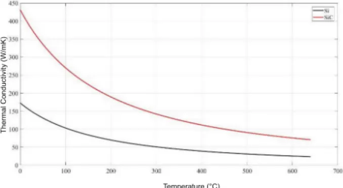
Fig. 1. Thermal conductivity of 100 µm SiC and Si substrates.
maximum values allowed for reliable earth applications and this in turns limits the device capabilities and performance.
GaN technology, already well exploited within PAs for terrestrial applications [4], is becoming interesting also for space usage, since it provides remarkably high power densities at the frequencies of interest, together with low losses (passive networks) and low-noise performance (receiver). GaAs, even if suitable for this frequency range, is strongly limited by low breakdown voltage [5]. GaN epitaxy can be grown on both SiC and Si substrates. SiC is characterized by extremely good thermal behaviour, that greatly mitigates the heat dissipation issue, but it is very expensive, also considering the limited number of high quality SiC substrate providers. On the other hand, the use of Si substrate, while penalizing thermal behaviour as shown in Fig. 1, would lead to lower cost with respect to SiC, which is an essential aspect for high volume of production, and it would allow, in the future, for the integration of RF and digital sub-systems on the same chip.
GaN/Si technology, compared to GaN/SiC counterpart, is therefore sensibly limited by thermal issues, in particular in case of space applications where temperature and voltage derating must be applied. In such scenario, the classical design paradigms usually adopted for power amplifiers must be reconsidered, targeting the best possible trade-off between desired output power and maximum allowable channel temperature. To this aim, it is crucial to have access to highly reliable and accurate thermal models.
This work will show the rationale behind a thermal-aware
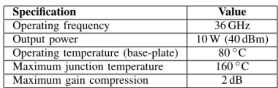
TABLE I DESIGN SPECIFICATIONS.
Specification Value
Operating frequency 36 GHz
Output power 10 W (40 dBm)
Operating temperature (base-plate) 80◦C Maximum junction temperature 160◦C Maximum gain compression 2 dB
design process, exploiting a 100 nm gate-length GaN/Si HEMT process from a commercial European foundry (OMMIC). The thermal model of the active devices will be discussed and compared to thermal measurement results, and the design of the output stage of a 10 W PA for space applications working at 36 GHz will be presented.
II. DESIGN EXAMPLE: 10 W GAN/SIKA-BANDMMIC The present work aims to highlight the differences between standard GaN/Si MMIC PA design, for terrestrial (e.g. telecom) applications, and a thermal-aware design approach, tailored instead for space applications. To contextualize the discussion a design example is considered, which main design requirements are summarized in Table I. The considered example is a narrow-band 10 W PA at 36 GHz, which is considered as a possible uplink frequency for next satellite communication applications. The maximum junction temperature of 160◦C is a typical value for GaN devices constrained to space applications and corresponds to a temperature 40◦C below the maximum value indicated by the selected manufacturer [3], [6], [7]. The example design focuses only on the final (power) stage of the PA, neglecting the design of driver stages, which would be required in a complete PA design to achieve usable gain levels. A simple but effective parallel combined strategy is considered [8] and, as an additional constraint, the maximum number of parallel combined device is set to 8 in order to limit the chip area and output combiner losses to a reasonable value. For the latter, a worst-case value of 1 dB is considered, which increases the output power requirement to roughly 12.6 W.
III. TECHNOLOGY
The selected process is the D01GH 100 nm gate-length GaN/Si HEMT process from OMMIC, a commercial European foundry. Process design kit (PDK) is available for this process, both for Keysight ADS (adopted in this work) and NI AWR-MWO design suites, including electro-thermal nonlinear model, electromagnetic model, components’ layouts and statistic data. The main features of the selected technology are summarized in Table II [6]: the high cut-off frequency of this process makes it suitable for application in Ka-band [9], [10].
Considering the given VDS,max= 15 V and IDSS = 1.3 mA/mm, an output power density around 5 W/mm is expected. When derating is applied to VDS, this value reduces to roughly 4 W/mm, which is a remarkable output power for Ka-band applications. However, when
TABLE II
FEATURES OF THEOMMIC D01GH GAN/SI PROCESS.
Parameter Value Derating
Cut-off frequency, fT 105 GHz Typ.
-Saturation current, IDSS 1.3 mA/mm Typ.
-Supply voltage, VDS 15 V Max. 75 % ⇒ 11.25 V
Breakdown voltage, VGDb 40 V Min.
-Junction temperature, Tj 200◦C Max. -40◦C ⇒ 160◦C
TABLE III
SIMULATED MAXIMUM OUTPUT POWER AT DIFFERENT JUNCTION TEMPERATURES. SUPPLY VOLTAGE11.25 V.
Device Pout Tj Pdiss PAE Notes
W/mm ◦C W/mm % 8x75 µm 5.6 250 4.0 45 max. Pout 4.2 200 3.0 47 max. Tj 3.0 160 2.1 47 max. derated Tj 8x50 µm 4.6 240 4.1 41 max. Pout 4.1 200 3.2 46 max. Tj 3.3 160 2.2 50 max. derated Tj
derating is applied also to the maximum junction temperature Tj, the achievable output power is clearly limited (see Table III), and a careful selection of the optimum load is required, as discussed in Section V. The results reported in Table III are based on ADS simulations, carried out adopting the thermal model discussed in Section IV below. Two different device sizes are compared: 8x50 µm (400 µm periphery) and 8x75 µm (600 µm periphery). In both cases the maximum output power exceeds the nominal value, however, the junction temperature is well above its maximum value, making such power levels practically unachievable and confirming that device heating is the actual limit of this technology. A maximum output power density around 4 W/mm is obtained, as expected, at the maximum thermal limit of the technology (Tj = 200◦C), indicating that a minimum periphery around 3.2 mm is required to achieve the required output power of 12.6 W. Conversely, at the maximum derated junction temperature (Tj = 160◦C), the achievable output power density decreases to only roughly 3 W/mm, thus increasing the minimum necessary periphery to 4.2 mm to reach the same output power.
IV. THERMAL MODEL
The OMMIC PDK comes with two different thermal models of its active devices. The first is a simplified static 1D heat flow model, while the second is a 3D thermal stack that can be used within a FEM-based numerical thermal simulator (e.g. HeatWave for Keysight ADS). Such simulators solve the dynamic Fourier heat equation using as heat source the electrical power dissipated within the device. The latter is computed from electrical simulations within an electro-thermal loop. This approach is more accurate and can account, for example, for the different finger temperatures within the same device. Despite this, the numerical effort it requires, in terms of simulation time, makes the simplified model the only viable approach for design and optimization purposes. Accurate
TBP Rth, Cth PRF,out PRF,in PDC Tj Tj Tj Tj Pdiss Pdiss Rth Cth ∆T Tj TBP
Fig. 2. Simplified thermal model of the active device and electrical equivalent.
electro-thermal simulations, on the other hand, can be used for a posteriori verifications during the most relevant design steps.
The simplified thermal model adopts a thermal resistance approach. As shown in Fig. 2, the device is modeled by a thermal resistance Rthdefined as
Rth= ∆T Pdiss
(1) where ∆T is the temperature increase due to power dissipation in the device, and represents the difference between the maximum temperature Tj reached in the device active region, right below the fingers (and considered the same for all the device’s fingers), and the base-plate temperature TBP. The dissipated power, when the transistor is operated in continuous wave, is given by
Pdiss= PDC+ PRF,in− PRF,out (2) The dynamic thermal behaviour is modeled by means of a thermal capacitance Cth, which gives, in combination with Rth a thermal time constant τth = RthCth. The resulting system is a single time-constant low-pass filter, as highlighted in Fig. 2. According to the foundry model, the thermal time constant is τth= 160 µs, thus the junction temperature reaches its maximum value TBP+RthPdissafter approximately 800 µs of continuous wave operation.
The simplified non-linear thermal model adopts a thermal conductivity with hyperbolic dependence on temperature [11], and implements a 1D Fourier heat equation, where heat is considered to adiabatically flow from the top surface, where the active device junctions generate it, to the bottom, where the heat sink keeps a constant base-plate temperature. This model correctly accounts for substrates built up with layers having different thermal properties, provided that all layers share the same functional temperature dependence on thermal conductivity [12]. In this case, in fact, the Kirchhoff
Fig. 3. Raman measurements: junction temperature of different devices as a function of the dissipated power density.
transformation validity is maintained across the several layers [13].
Introducing the total thermal resistances of the substrate evaluated at the reference temperature T0a (superscript a denotes absolute temperatures in kelvin) as
Rth,REF(T0a) = H A · 1 Kth(T0a) (3) where H is the substrate thickness, A the area of the device footprint and Kth(T0a) the thermal conductivity at T0a , we have Tja= TBPa expRth,REF(T a 0)Pdiss Ta 0 (4) where TBPa is the (absolute) base-plate temperature. The OMMIC PDK gives, for any device periphery, the value of Rth,REF at 20◦C (293.15 K).
A. Thermal model verification
The validity of the simplified thermal model is verified both through 3D electro-thermal simulations and through experimental Raman characterization [14], [15].
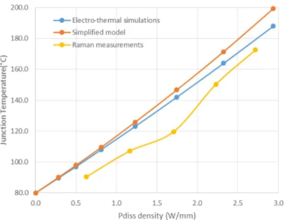
The Raman characterization of the devices has been performed monitoring the Raman shift of the Si layer below the GaN layer in the channel region [16]. A calibration law is extracted first, with no bias applied to the device, to correlate Raman shift to temperature. Then, in the dissipation phase, the temperature of the base-plate is fixed (80◦C), and the power dissipated in the device is varied by changing the bias voltage. In order to correlate the measured temperature in the Si layer to the junction temperature in the GaN channel region, the 3D thermal simulation results are exploited. Raman measurements were carried out on different active device samples made available from the foundry, namely the 8x50 µm, the 6x50 µm and the 4x50 µm devices. The measurement results are compared in Fig. 3.
Finally Fig. 4 reports the comparison between the results obtained with the electro-thermal simulation, the Raman characterization and the simplified model predictions, for the
Fig. 4. Junction temperature as a function of dissipated power density: comparison between electro-thermal simulations, simplified model predictions and Raman measurement results (8x50 µm device).
8x50 µm device. The results are in very good agreement, with the simplified model showing slightly higher temperatures than the other, more accurate, models. Therefore, despite the approximations, the simplified model is a very effective tool for quick junction temperature estimation for MMIC design purposes.
B. Crosstalk effect
Equation (4) is valid for a single isolated device. When more devices must be combined in parallel in a small chip area, as is usually the case for Ka-band PAs, the device heating due to neighbour devices (crosstalk effect) must be accounted for. This can be done by adjusting (increasing) the value of Rth,REF, but 3D electro-thermal simulations are required to find the actual value of this equivalent reference thermal resistance for the actual device configuration considered in the PA under development.
Fig. 5 reports, as an example, the 3D thermal simulation results for 4 parallel combined 8x75 µm devices. As can be noted the heat spread through the output combiner is negligible and the cooling effect of the via holes at the source terminals makes the devices almost thermally decoupled. In fact, an increase of only 2.2 % of Rth,REF is required to correctly account for thermal crosstalk.
V. THERMAL-AWARE DESIGN OF THE10 W KA-BANDPA The results of Fig. 4 highlight that the junction temperature is the most stringent limit of this technology, which bounds the maximum allowable dissipated power to approximately 2.2 W/mm at TBP = 80◦C.
Performance of microwave devices depends on the selected load termination. Dissipated power, and thus junction temperature, is not an exception, therefore, when moving in space applications framework, the optimum load is no more the one that gives the maximum output power, like in classical PA design, but it must be selected as the best compromise between output power and junction temperature. Moreover, power gain, efficiency and eventually output mismatch should
Fig. 5. 3D thermal simulation results for 4 parallel combined 8x75 µm devices.
be considered, since an optimum trade-off typically exist among all these device performance. To find this optimum termination, simulated thermal load-pull maps must be drawn, which give the most complete and straightforward information on optimum load selection.
In Fig. 6 the load-pull simulation results for the 8x50 µm and 8x75 µm devices are compared. Contours are referred to 1 dB gain compression. The junction temperature contours are computed from the CW dissipated power with (4) adopting the Rth,REF values obtained from 3D simulations for 8 parallel devices, thus slightly higher than the values given in the PDK (see Section IV-B). This results confirm that, targeting a minimum output power of 32 dBm, the 8x50 µm device can be used in a classical PA design (ΓL,opt laying on the Tj = 200◦C contour), while the larger 8x75 µm device is required when dealing with the Tj = 160◦C limit posed by space derating. Fig. 7 reports a more detailed load-pull chart for the 8x75 µm device, showing also PAE (contours with 1 percentage point step) and output mismatch contours (2.5 dB step). The latter are computed as
Mismatch = 20 log10 ΓL− Γ∗out 1 − ΓLΓout (5) and represent a good estimation of the PA output return loss. From these results the optimum load can be selected as ΓL,opt = 0.82ej161
◦
, which guarantees the best trade-off among all the considered performance, as shown in Table IV. Figure 8 shows the large-signal CW simulations results at 36 GHz of the device terminated with the selected optimum load, the temperature increase ∆T is defined as Tj − TBP, where TBP = 80◦C.
To complete the design of the final stage, an output combiner network matching ΓL,opt at each device output to a common 50 Ω load, has been developed, as shown in Fig. 9.
(a) 8x75 µm device (b) 8x50 µm device Fig. 6. Load-pull results at VDS= 11.25 V, 1 dB compression.
Fig. 7. Load pull contours at 1 dB compression for the 8x75 µm device, VDS= 11.25 V.
The performance of this final stage are shown in Fig. 10: the devices are well matched to ΓL,opt and output power of each single device is around 32 dBm. The output combiner losses are within 0.85 dB, thus the achieved output power is above 40 dBm at a gain compression slightly above 1 dB. The associated junction temperature is within the 160◦C limit, thus demonstrating the potentiality of the selected GaN/Si technology for high-frequency space applications.
VI. CONCLUSION
This work shows a thermal-aware MMIC PA design approach that should be adopted when designing GaN/Si
TABLE IV
PERFORMANCE OF THE8X75 µM DEVICE AT36 GHZ AND1DB
COMPRESSION. Feature Value VDS 11.25 V TBP 80◦C ΓL 0.82ej161 ◦ Pout 32.6 dBm Tj 160◦C Gain 4.2 dB PAE 47 % Output mismatch -13 dB
Fig. 8. Large-signal CW simulation results for the 8x75 µm device, VDS= 11.25 V.
Fig. 9. Layout of the 8x8x75 µm final stage of the designed PA.
amplifiers for space applications. On one hand, it is demonstrated how space thermal requirements limit device performance in case of GaN/Si technology, thus requiring larger peripheries for the same targeted output power. On the other hand, following a thermal load-pull approach, it is also demonstrated how, with proper selection of the load termination, GaN/Si technology is able to achieve competitive
results at Ka-band also when enforcing space derating rules. REFERENCES
[1] European Space Agency, “Satellite frequency bands,” Oct. 2018. [Online]. Available: {https://www.esa.int/Our\ Activities/ Telecommunications\ Integrated\ Applications/Satellite\ frequency\ bands}
[2] C. Ramella, A. Piacibello, R. Quaglia, V. Camarchia, and M. Pirola, “High efficiency power amplifiers for modern mobile communications: The load-modulation approach,” Electronics (Switzerland), vol. 6, no. 4, p. 96, Dec. 2017.
[3] European Cooperation for Space Standardization, “ECSS-Q-ST-30-11C Rev 1 - Space product assurance - Derating EEE components,” Oct. 2011. [Online]. Available: {https://escies.org/download/ webDocumentFile\%3Fid\%3D58751}
[4] V. Camarchia, R. Quaglia, C. Ramella, and M. Pirola, “Power amplifier mmics for 15 ghz microwave links in 0.25 ¨um gan technology,” in 2017 Integrated Nonlinear Microwave and Millimetre-wave Circuits Workshop (INMMiC), Apr. 2017, pp. 1–3.
[5] T. Fersch, R. Quaglia, M. Pirola, V. Camarchia, C. Ramella, A. J. Khoshkholgh, G. Ghione, and R. Weigel, “Stacked gaas phemts: Design of a k-band power amplifier and experimental characterization of mismatch effects,” in 2015 IEEE MTT-S International Microwave Symposium, May 2015, pp. 1–4.
[6] OMMIC, “U-GaN Design Manual,” Nov. 2018.
[7] European Space Agency, “GaN Reliability Enhancement and Technology Transfer Initiative (GREAT2).” [Online]. Available: {https://escies.org/download/webDocumentFile?id=63411}
[8] R. Giofr`e et al., “A comprehensive comparison between gan mmic doherty and combined class-ab power amplifiers for microwave radio links,” International Journal of Microwave and Wireless Technologies, vol. 8, no. 4-5, p. 673–681, 2016.
[9] A. Gasmi et al., “10W power amplifier and 3W transmit/receive module with 3 dB NF in Ka band using a 100nm GaN/Si process,” in 2017 IEEE Compound Semiconductor Integrated Circuit Symp. (CSICS), Oct 2017, pp. 1–4.
[10] A. Cidronali et al., “System Level Analysis of Millimetre-wave GaN-based MIMO Radar for Detection of Micro Unmanned Aerial Vehicles,” to appear in 2019 Photonics Electromagnetics Research Symp. (PIERS), Jun. 2019.
[11] W. Joyce, “Thermal resistance of heat sinks with temperature-dependent conductivity,” Solid-State Electronics, vol. 18, no. 4, pp. 321 – 322, 1975. [Online]. Available: http://www.sciencedirect.com/science/article/ pii/0038110175900854
[12] F. Bonani and G. Ghione, “On the application of the kirchhoff transformation to the steady-state thermal analysis of semiconductor devices with temperature-dependent and piecewise inhomogeneous thermal conductivity,” Solid-State Electronics, vol. 38, no. 7, pp. 1409 – 1412, 1995. [Online]. Available: http://www.sciencedirect.com/science/ article/pii/003811019400255E
[13] O. A. Ezekoye, Conduction of Heat in Solids. New York, NY: Springer New York, 2016, pp. 25–52. [Online]. Available: https://doi.org/10.1007/978-1-4939-2565-0 2
[14] D. Tuschel and F. Adar, “Raman thermometry,” vol. 31, pp. 8–13, 2016. [15] G. Zhang, S. Feng, J. Li, Y. Zhao, and C. Guo, “Determination of channel temperature for AlGaN/GaN HEMTs by high spectral resolution micro-raman spectroscopy,” Journal of Semiconductors, vol. 33, no. 4, p. 044003, Apr. 2012. [Online]. Available: https: //doi.org/10.1088%2F1674-4926%2F33%2F4%2F044003
[16] S. Choi, E. R. Heller, D. Dorsey, R. Vetury, and S. Graham, “Thermometry of AlGaN/GaN HEMTs Using Multispectral Raman Features,” IEEE Trans. Electron Devices, vol. 60, no. 6, pp. 1898–1904, Jun. 2013.